Week 6
Echo Hello-World Board
PCB Design Software: Eagle
Machine: MODELA MDX-20 (Software: Fab modules)
Components and Tools
- PCB (FR-1) x 1
- Double-sided tape x 1
- Mitsuwa Paper Cement Solvent x 1(Amazon.jp)
- Scraper x 1
- Digital Multimeter x 1
- Soldering Iron x 1
- Solder x 1
- Desoldering Braid x 1
- Tweezers x 1
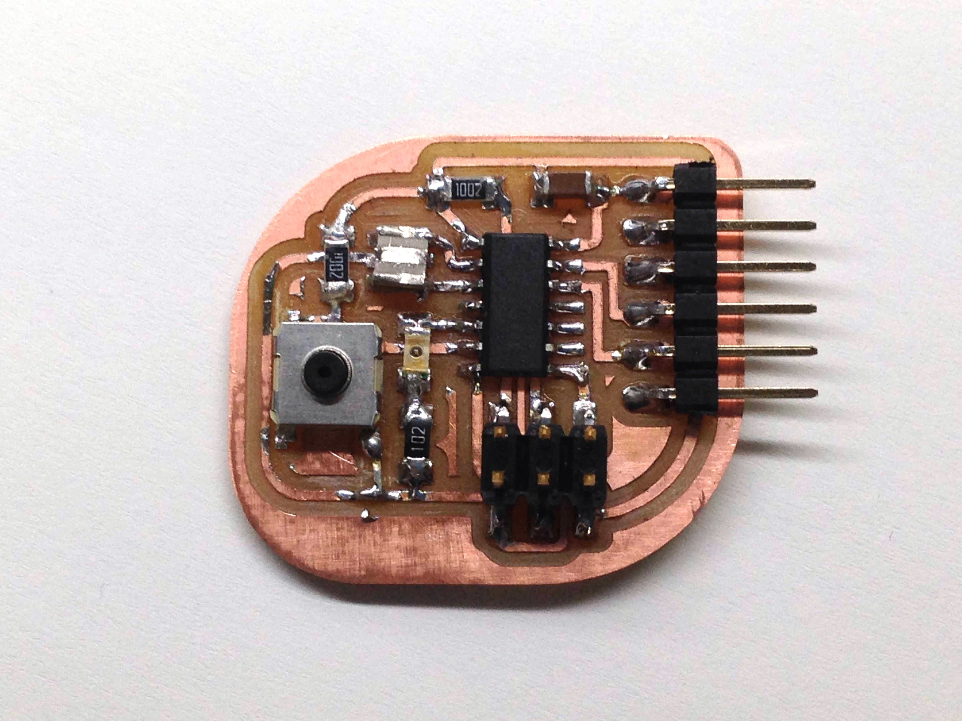
This week I made an echo hello-world board that includes an led and button. In addition to the fab.lib (right click and Save Link As...to download) I also used two libraries which I received from my instructor Mio-san (because I was going to use a button that was purchased in Japan).
(all photos can also be viewed here)Since there are a lot of libraries in Applications Eagle lbr, instead of just adding my libraries to the directory, I created a file called libraries in Applications Eagle and moved the existing lbr file and the downloaded library files in there, to differentiate the existing libraries from the ones I added. Then I changed the directory settings in Eagle and selected the libraries in the Control Panel. From File, create and name a new Project. When you create a new Schematic file under that project, the Schematic window will open.
I like using the command line instead of clicking on the icons.
(Type the command, then press enter)
- grid (or gr) : change the settings for the grid (turn on/off the grid and change its size etc.)
- add (or ad) : choose components from library and place them by clicking
The screen shots below are all of the components I used. (all photos can also be viewed here)
- copy (or cop) : click component to copy it
- delete (or de) : click and delete anything
- rotate (or ro) : click component to rotate it 90 degrees
- group (or gro) : click and drag to select several components
- move (or mov) : click component to move it. For moving several components at once 1: Select the components with group, 2: move, 3: Right click any empty area, 4: Select Move: Group
- net (or ne) : connect components by clicking. (After netting you can move the component around to make sure it's connected correctly.)
- name (or na) : click component to rename (i.e. XTAL)
- value (or va) : click component to write its value (i.e. 20MHz, 10k). “Do you want to change it anyway?” Select yes.
- erc (or er) : to check for errors on the Schematic
Connecting all of the components together can get a little messy. You can also Label Net Stubs as I did for ISP and FTDI. (1: Make short nets for each of the pins you want to connect. (Single click to start a net. Double click to stop) 2: Assign names to the nets using label 3: Give the nets you want to connect the same name, “Connect ~ and ~ ? Select yes.) 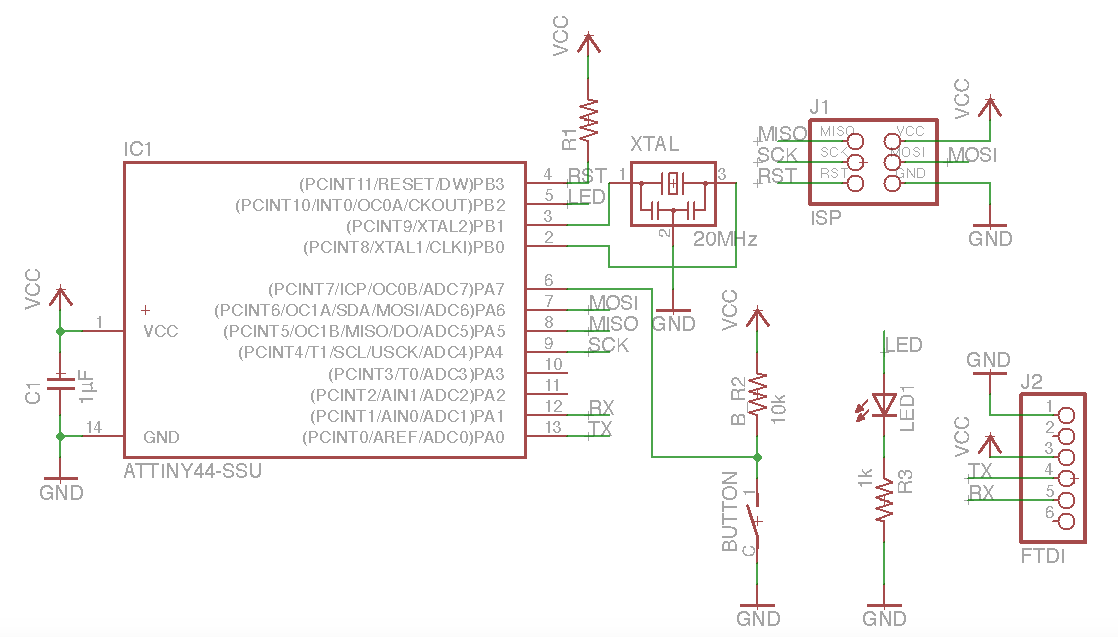
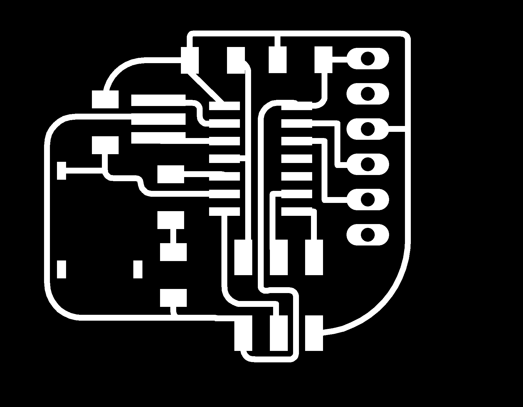
Once you're done connecting everything, click  (on the top left) to generate the board (Create for schematic? Select yes). All of the components will appear bundled up at the left corner. Now it’s time to place out the components (move) and draw the circuit's paths (route).
- route (or rou) : click to draw routes. Right click to change the bend style.
- ripup (or rat) : click to delete routes
- ratsnest (or rat) : changes paths between components to the shortest possible
- show : highlights the chosen components (i.e. show vcc, show gnd)
- move and click the sides of the white borderline to change the board's canvas size
- polygon (or pol) : at the top toolbar, change the layer from 1 Top to 48 Document. Draw the outline of the board.
- drc (or dr) : Select Clearance, change all values to to 0.4mm, and select check. move components or routes that are too close. (decreasing the grid’s size will make it more easier to slightly move them)
- display (or dis) : select which layer to export.
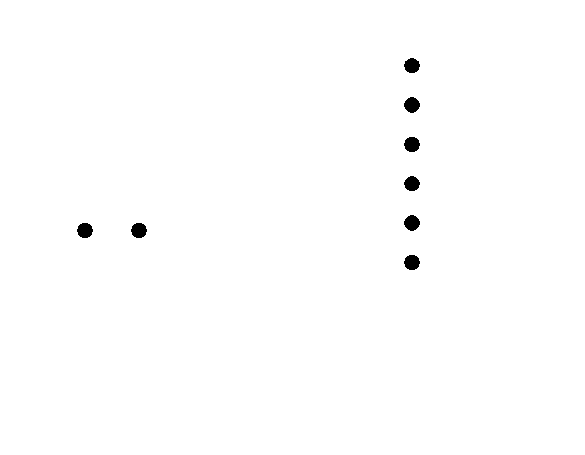
Traces: Select 1 Top and 17 Pads
Holes: Select 17 Pads 20 Dimension
Outline: Select 48 Document
From the menu bar select File Export Image. Name the file, select monochrome, change the resolution to at least 800dpi (1200dpi for the Traces) and export.
While the Modela was milling the traces I was staring at the image of my circuit and noticed there was a small mistake. The button wasn’t connected to ground. Woops! I found a broken led, cut a small piece off the leg and soldered it on to make the connection.