
06 Electronics Design
Assignment
- Draw the schematic for the Hello-world board
- Add a button and LED to the board
- Create the board
Journey
- Eagle is a schematic layout and printed-circuit board design software offered by CADSoft. In the free or light version, the creation of the board is limited to
- a useable board area of 100x80mm
- two signal layers (top and bottom)
- the creation of only 1 sheet using the schematic editor
- Before starting the actual process, I went through 4 very useful tutorials by Sparkfun: I strongly suggest that anyone attempting Eagle and PCB design go through these tutorials first, it saves a lot of time.
- I also found that although Eagle is GUI-driven, it is very useful to use the command-line entry to execute the commands (EAGLE commands) (You will need to type in the whole word and press ENT in order for the command to work.
- In order to use the components in the FabAcademy, the library fab.lbr is added to the Eagle library and used extensively in the design. When using OSX/Linux, separate the library directories using a colon (':') instead of a semicolon.
- Place an A4 Frame at the cross-hairs (origin)
You can change the the Title, Document number and Author by changing the properties of the frame. - I redrew the schematic as presented from Neil's initial board and added the LED and switch using the fabLab.lbr
- Useful commands:
- Use the ADD command to place parts on the schematic.
- Use NAME/VALUE to change the properties of the parts.
- Use NET <net-name> to draw the connections between the parts. It is useful to use the net-name as it saves effort naming and labeling it later.
- Use LABEL to attach labels to the nets.
- Use MOVE (and associated RClick to ROTATE) the parts.
- Use GROUP and select with the mouse a selection of parts which you can operate on (use CTRL-RClick to activate command)
- Use SMASH to de-link the NAME text from each of the parts so that you can move/rotate for better display
- Use the ALT (CTRL-ALT for Linux) to perform fine movements between the grid placements.
- A resistor (499 Ohm) is added to limit the current through the LED (though not necessary with careful programming of the CPU which has internal pull-up resistors). 499 Ohms is not the typical resistor I would use (330 Ohm would be better), but since I have the SMD version on hand, it would suffice.
- Similarly, a resistor (10K Ohm) is used to limit the current flowing to ground when the switch is pressed.
- Building a board with only a LED and switch added, seems a waste, so I redesigned the board to allow the lines of PA2-PA7 to be used as I/O lines when the jumpers are in place on JP2 and when the ISP is removed.
- In the creation of the board, the following DRC rules were used:
Trace size: 12mil
Trace to Trace: 16mil
Trace to Pad: 16mil - After the creation of the board, I changed the size of the trace and using rip-route commands, replaced the 12mil traces with 16mil wherever possible to make routing and production more reliable.
- (Tip: Use RIP * to rip up all routes. You could substitute '*' with the name of the net to rip up.
- The DRC rules are used to check the board after routing, all errors are checked and cleared before the next stage
- We are now ready to use the CAM processor to create the necessary files for the milling process. The CAM processor needs to load in the GERB274X paramters. The following files are created for each of the layers:
Name               Layer(s)                   File Extension
Board Outline      20 Dimension                   .otl
Component Side     1 Top, 17 Pads, 18 Vias        .cmp
Solder Side        16 Bottom, 17 Pads, 18 Vias    .sol
Silk Screen        20 Dim, 21 tPlace, 25 Names    .plc
- We need to inspect the Gerber output before milling, this is done using a Gerber Viewer (e.g. gerbv) which allows you to look at the different layers independently. Gerbv is available for Linux, MacOSX and Windows. The following shows the installation and use for Ubuntu
Gerber file viewer: gerbv
Install in Ubuntu:
	sudo apt-get install gerbv
	Open a New project
	Use File > Open Layer(s) to load the Eagle CAM job output
	View the job
	Save your project
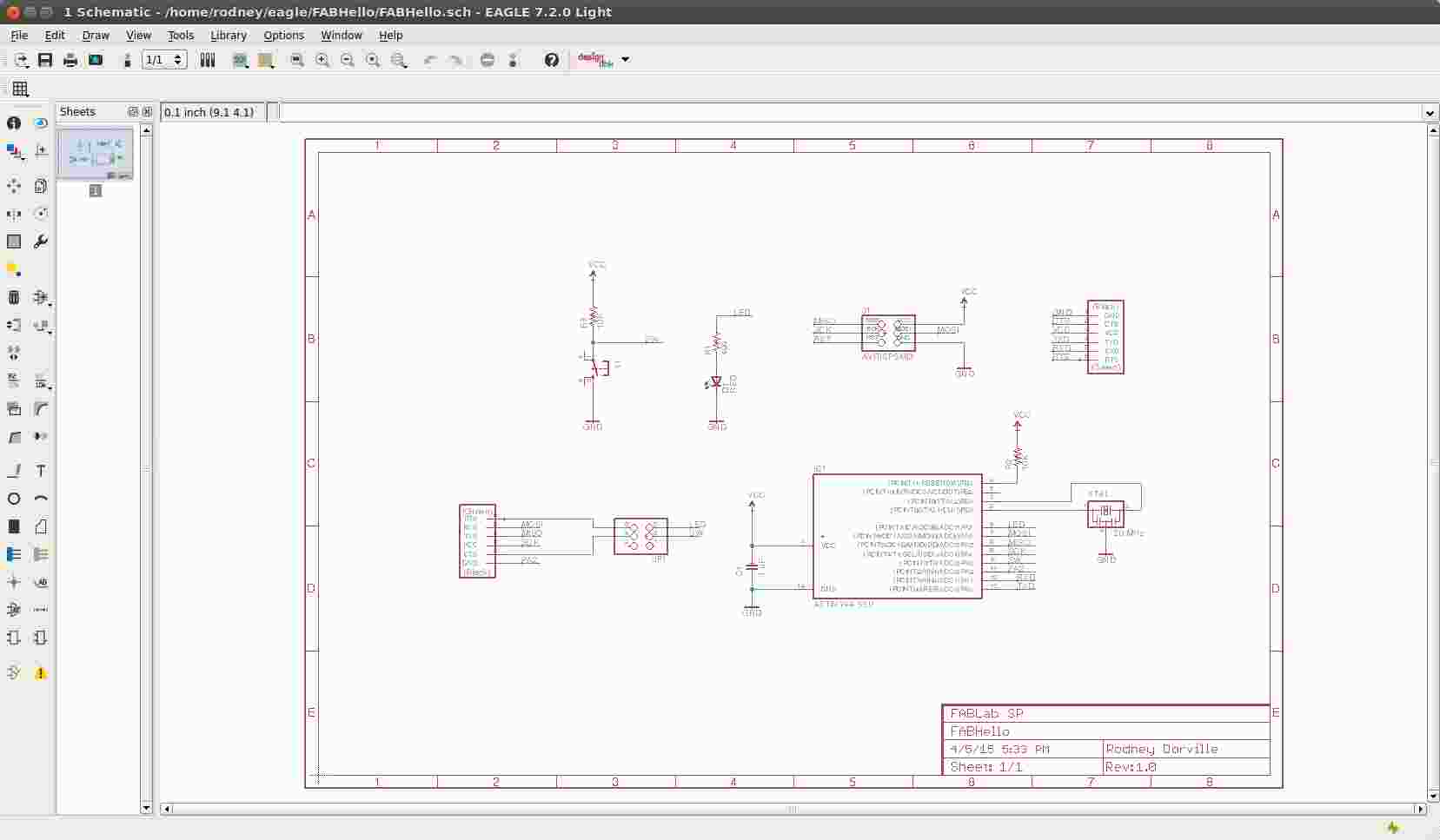 FABHello Schematic Capture
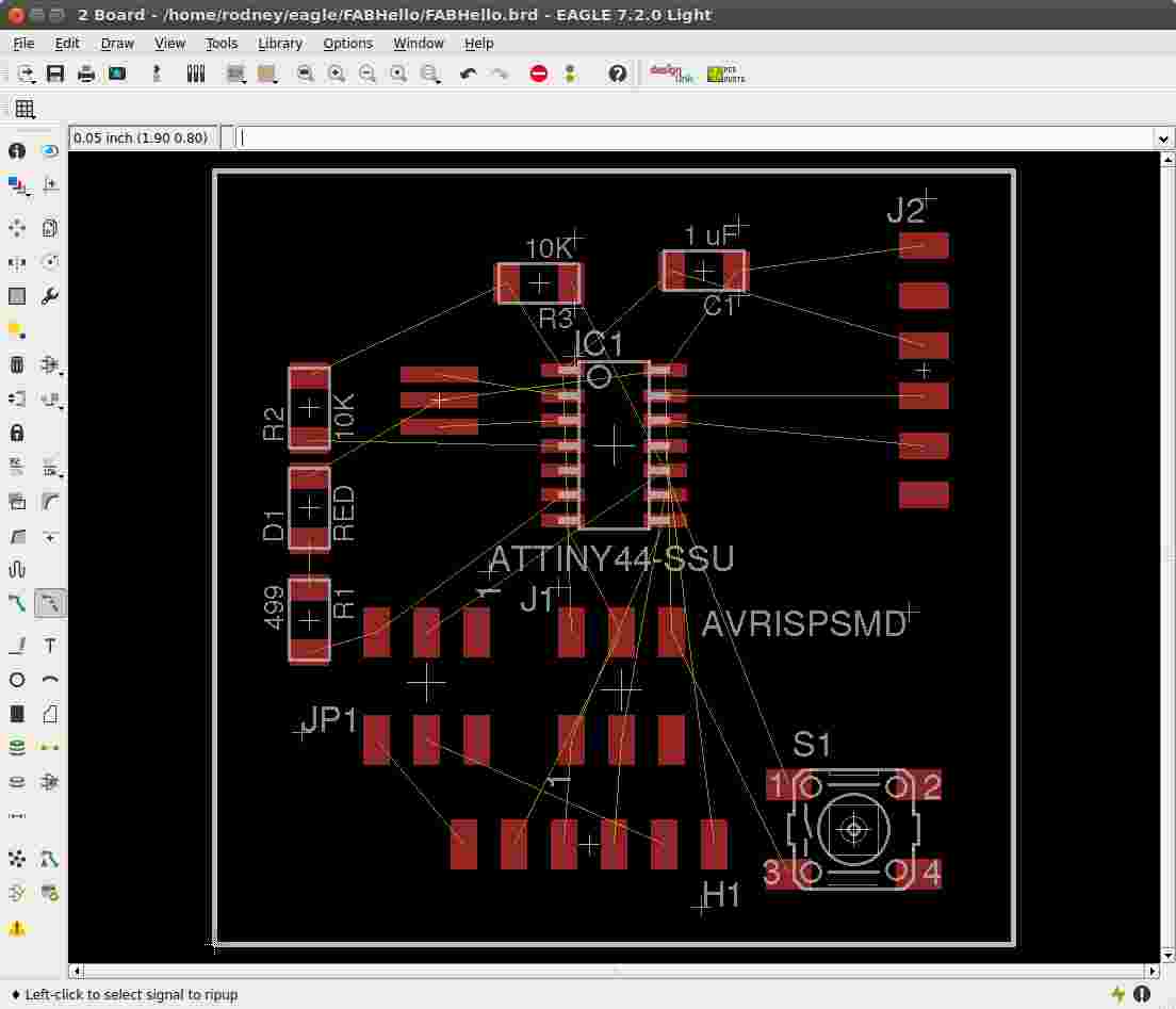 FABHello placement with ratsnets
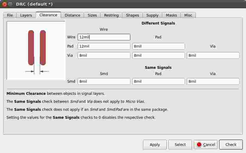 Design Rules Check spacing
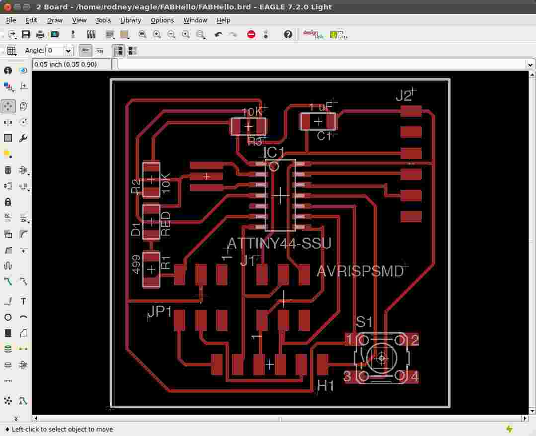 Completed board layout with traces
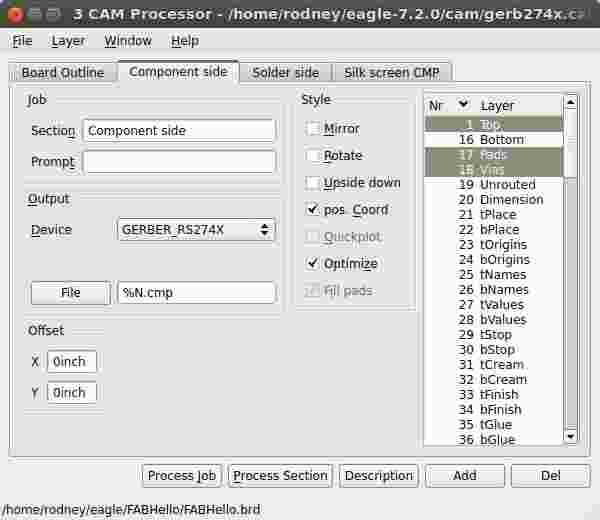 CAM processor for milling
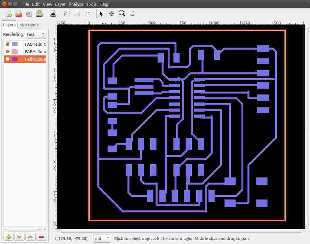 GerbV checking of output
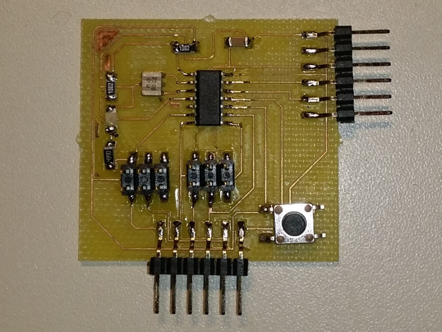 Soldered & completed board
Circuit Layout: 06_FABHello.pdf
Schematic: 06_FABHello.sch
Board Layout: 06_FABHello.brd
Gerber: 06_FABHello.cmp, 06_FABHello.otl, 06_FABHello.plc
Correction!
- When I tried to program the board, the IDE kept returning an error. I checked the programming with another board design and found out that the problem lies with my design, so back to manual troubleshooting
- Manual troubleshooting:
- Checked voltages Vcc and Gnd - ok
- Checked polarity of LED - ok
- Checked continuity of tracks - failed!
- Solution was to manually solder in a jumper wire for the RST net at the header, once done, the board worked perfectly.
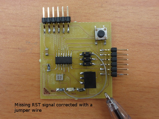
RST corrected with jumper wire
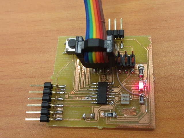
Success!
If you look at later weeks, I have better designs and boards for ATTiny44.
Fixed Eagle files: Fixed Schematic, Fixed Board
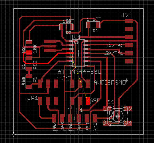
Fixed Board showing error
Reflection
- Schematic capture & board layout is lots of fun. So much has changed since the old Mentor-Graphics system of the '90s. Most of the packages have been created into libraries and it makes it so simple.
- Knowledge of Command-line input is essential and efficient to the schematic or layout, use it!
- Use ERC and DRC to check your design
- Use NET <net-name> when drawing nets, makes troubleshooting easier
References
- CADSoft Eagle PCB Design Software
- Sparkfun - How To Install Eagle
- PC Board Plotter LPKF Protomat S103
- EagleCadWorkshopNotes
- CAM processor for Eagle
- GerbV - Gerber file viewer
Not being of a artistic mind, I have shamelessly borrowed this template (simpleStyle_8) from html5webtemplates, in recognition of a simple, cool and functional webpage design.