

Week 6. Electronics design
The assignment for this week of the FabAcademy was redraw the echo hello world board, adding at least a button and a LED, that will be later programmed in following weeks. To design the board, during the class, several software solutions were presented.
During my period at the university and later at my work, I used some popular (but not free and quite expensive in fact) electronics design software as OrCAD or Altium. That is the reason this weeks I decided to go a step further, and design my circuit not in Eagle which is very popular but very similar to the ones mentioned before but in a language scripting software.
As I knew that Kokopelli could be used also to design PCB, and I had some experience with it, I decided to go for it.
After some research in the web, I found this nice tutorial from Francisco about how to design PCB in Kokopelli. Unluckly, it stated that this tutorial was only valid for kokopelli 0.05, and the one I had downloaded was the version 0.2. Although running the command kokopelli -r is supposed to run a retro mode, it was not running for me.
At this moment I thought about going back and use Eagle... but I didn't. In kokopelli's git repository you could find this example of the FabISP design, demonstrating kokopelli's pcb library design. After looking carefully at it and making some tests, I learned how to use it.
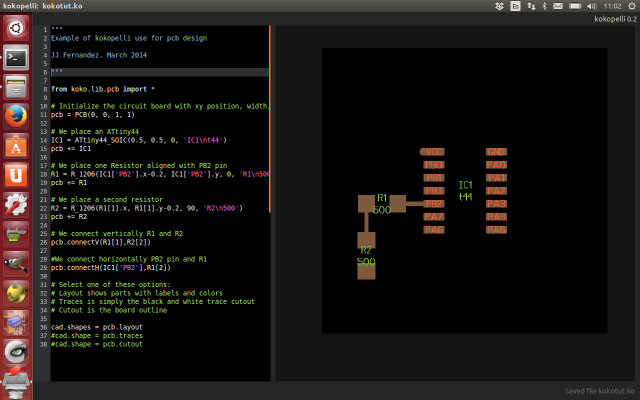
Mini tutorial of designing a pcb with kokopelli 0.2
To design a pcb with kokopelli, the first thing you must do is to import kokopelli's pcb library, where some components are defined:
Then, you define your board, where you later will place all the components and wires. The parameters
of this function are the x and y position of the board, the width and the height.
You can place any of the components present in the library, or you can create new ones.
To see the components available in the library, you can see them in the path
/usr/local/bin/koko/lib/pcb.py. In the code
below, we place a Attiny44 microcontroller and two 1206 resistor. The parameters set are the
x and y position, the rotation of the component and the label to be displayed.
You can also get the x or y position of any component with the .x or .y sentences.
pcb += IC1
# We place one Resistor aligned with PB2 pin
R1 = R_1206(IC1['PB2'].x-0.2, IC1['PB2'].y, 0, 'R1\n500')
pcb += R1
# We place a second resistor
R2 = R_1206(R1[1].x, R1[1].y-0.2, 90, 'R2\n500')
pcb += R2
Once you have all the components, it is time to connect them. To do it,
you can use two different functions, pcb.connectH() or pcb.connectV() depending if
you want to wire in horizontal or vertical. Then, you must also define the path of the wire, adding
as many points as you consider necessary.
pcb.connectV(R1[1],R2[2])
#We connect horizontally PB2 pin and R1
pcb.connectH(IC1['PB2'],R1[2])
Once you have all your components and connections ready, it is only remaining to display
them, or only display the traces if you want to export them to be milled. Just place one of the lines
below depending on what you want to display.
cad.shape = pcb.traces
cad.shape = pcb.cutout
And here you can see the board we have designed. You can also
download the file.
|
|
Adding components to the library
After I learned how to use Kokopelli, it was time to redesign the hello world board. Unluckily, not all the components needed were available at the library, so I needed to create new ones.
I opened the pcb.py file and, after some time to get used to the language, I created the new components needed. Anyway, I still don't know why, my design in kokopelli does not understand this new components... I am a bit fuzzy about this, and although I made many tests, I still do not know the reason.
What finally did work to me, although I know it is not the best way to do it, it was just to copy the whole content of the pcb.py file and paste it on my .ko design. You could find below the components I created:
The crystal
class XTAL_EFOBM(Component):
pins = [Pin(-0.053, 0, _pad_XTAL_EFOBM),
Pin(0, 0, _pad_XTAL_EFOBM),
Pin(0.053, 0, _pad_XTAL_EFOBM)]
prefix = 'X'
The button
class button_6mm(Component):
pins = [Pin(-.125,.08, _pad_button_6mm,'4'),
Pin(-.125,-.08, _pad_button_6mm,'2'),
Pin(.125,-.08, _pad_button_6mm,'1'),
Pin(.125,.08, _pad_button_6mm,'3')]
prefix = 'BT'
The led
pins = [Pin(-0.06, 0, _pad_1206, 'A'), Pin(0.06, 0, _pad_1206,'C')]
prefix = 'D'
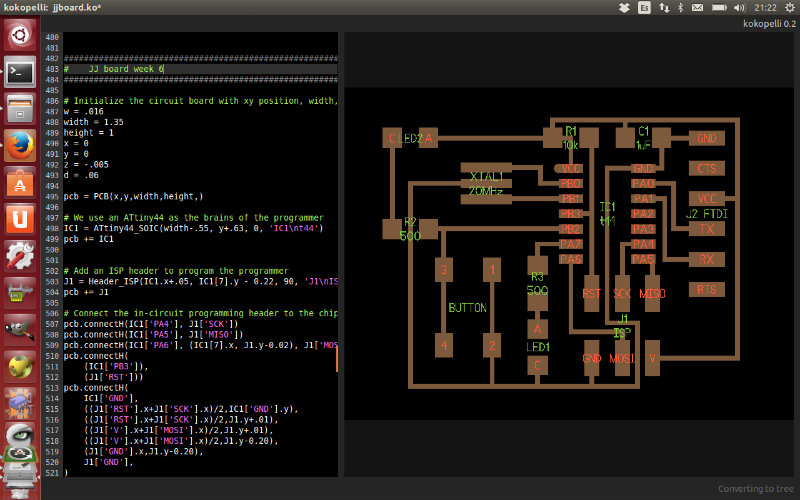
My hello world custom design
As I had all the components I needed and I knew how to design electronics in kokopelli, it was the perfect moment to design my custom hello world board. Before thinking about what components I would add and their disposition, I just tried to replicate Neil design but in kokopelli. You can see here my replica of it and download the hello world board in kokopelli.
|
|
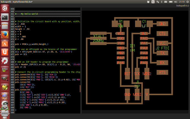
Once I have draw the hello world board design, it was time to customize it with a LED and a button at least.
I decided to include the button but two LEDs: one connected to an output port of the microcontroller but a second one connected to the button. My idea is that the LED conencted to the button will be only driven by hardware, while the LED connected to the microcontroller will be driven by software, so I could program it to do different things.
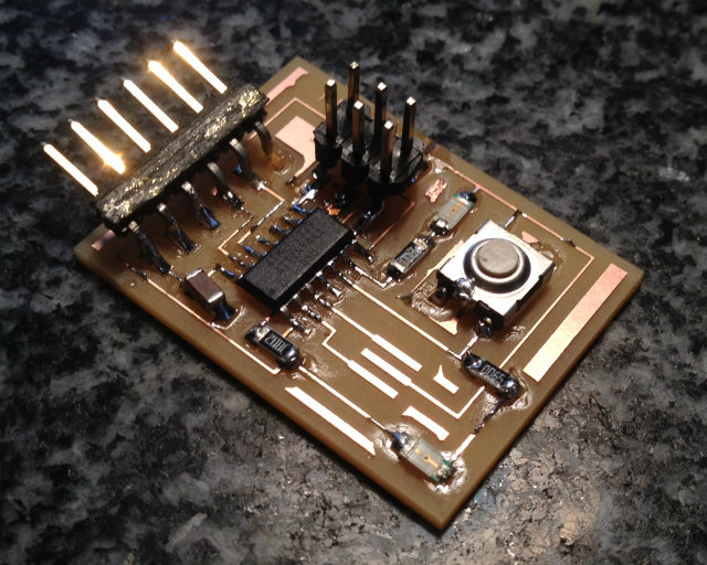
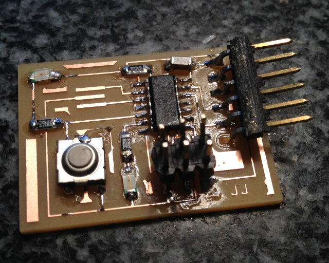
You can download my custom board in kokopelli and you can see a snapshot.
|
|
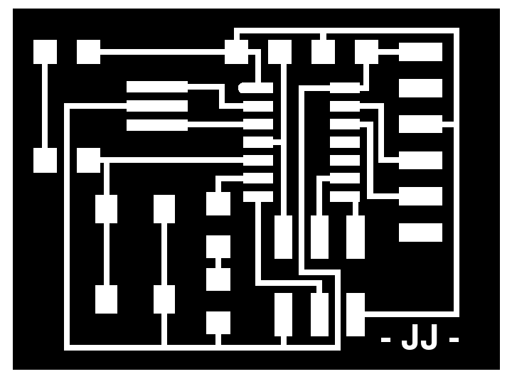
And finally export a .png file with the traces and another one with the contour of the board so we can make it later in the Roland Modela.
Milling and assembling my hello world board
My design is finished, so it is the moment to mill and assemble my board. To do this, it was useful to me to come back and remember what we did in the Electronics production week. To summarize:
|
Load the png file with the traces of the paths you want to create and mill it with the 1/64" mill. |
|
|
|
Load the png file with the contour of the board and mill it with the 1/32" mill. |
|
|
|
The Modela has milled your board. |
|
|
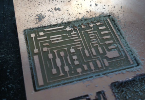
Once your board is milled, it is time also to remember what was done on Electronics production week and solder or the components in the board. You can see in the image below my board finished.
You can see in the image that I have not placed the resonator. This is because it was out of stock in the FabLab inventory. I will see if I can get it before programming the board, and if not, I will try to modify the code and use the internall oscillator.
|
|
|
In the pictures above I observed something that I did not observed when I was doing it. For soldering the components I used a solder that I have at home and I purchased some time ago. I think it is not regulating properly its power. As you can see in the images, it almost burnt my board!!