Appearance
Electronic design
In this session I have learned that the process of designing a PCB includes defining project requirements, selecting components, using design software to create schematics and layouts, generating 3D manufacturing files for the circuit board.
Hero shot of the Designed PCB.

Group Work 2023 & 2025- Multimeter and Oscilloscope
Assignment: Use the test equipment in your lab to observe the operation of a microcontroller circuit board. Our lab has a multimeter and an oscilloscope as test equipment, the details are shown as below.
Multimeter 2023: we use a SNDWAY SW-890C multimeter. It is a digital multimeter that offers a range of functions for measuring various electrical parameters.

The specifications include below:
The key features:
- True RMS Measurement: Accurate measurement of both AC and DC voltage and current, even with non-sinusoidal waveforms.
- Manual Range Selection: Allows you to manually select the range for voltage, current, and resistance measurements.
- Multiple Functions: Measures voltage (AC/DC), current (AC/DC), resistance, diode, continuity, capacitance, frequency, and temperature.
- Input Protection: Rated for CAT III 1000V and CAT IV 600V, providing safety during measurements.
- Large LCD Display: Clear and easy-to-read display for accurate readings.
- Additional Features: Includes a hold function, max/min function, and audible continuity beep.
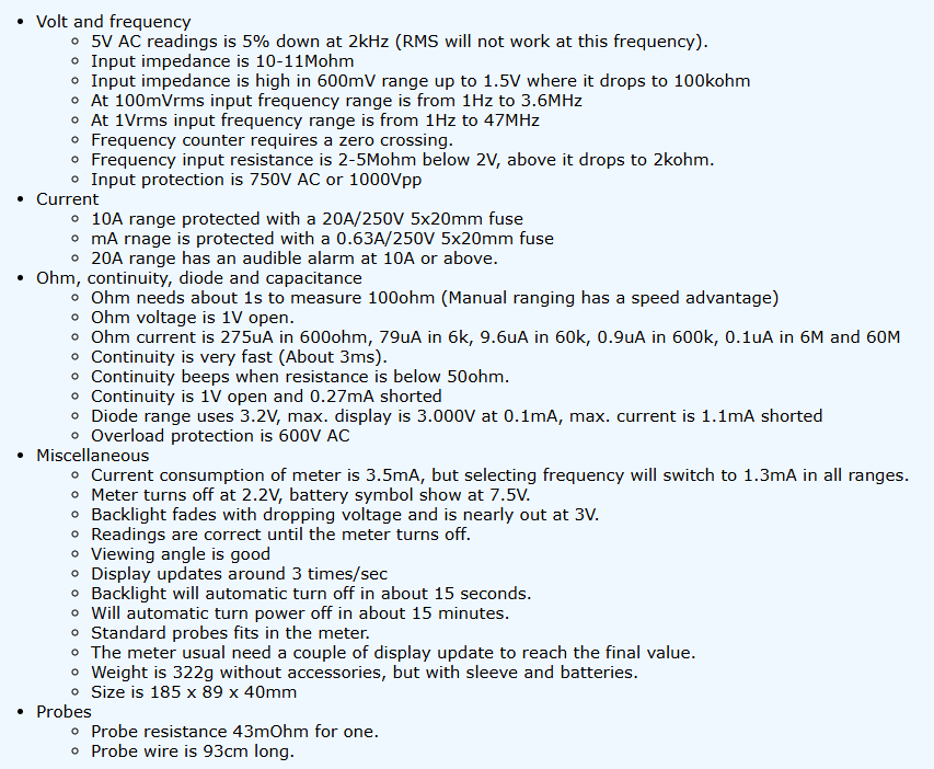
Multimeter 2025: we use a VICTOR VC9806+ multimeter.
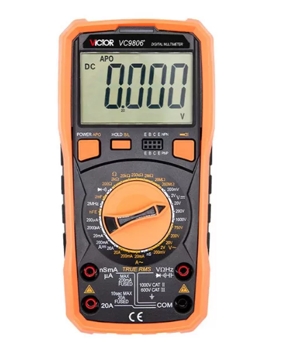
The specifications include below:
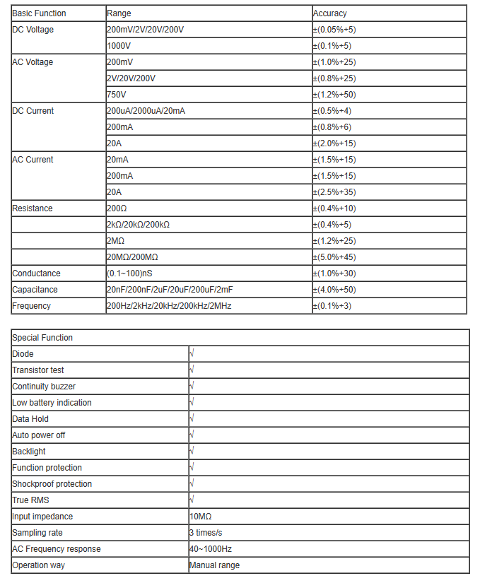
🔧 Core Specifications
- Display: 4½-digit LCD (max count: 19,999)
- Measurement Modes:
- DC Voltage: 200mV – 1000V (±0.05% accuracy)
- AC Voltage: 200mV – 750V (±1.0% accuracy)
- DC Current: 200µA – 20A
- AC Current: 200µA – 20A
- Resistance: 200Ω – 200MΩ
- Capacitance: 20nF – 2mF
- Frequency: 200Hz – 2MHz
- Temperature: -20°C to 1000°C / -4°F to 1832°F
- Sampling Rate: 2–3 times per second
- Input Impedance: 10MΩ
- True RMS: Yes
- Manual Ranging: Yes
Oscilloscope 2032 & 2025: we use a RIGOL DS2102A oscilloscope. An oscilloscope is a vital tool used to visualize and analyze electrical signals in real-time. It captures voltage changes over time, displaying the waveform on a screen. This allows for precise measurement of various signal parameters, such as amplitude, frequency, and timing characteristics. Oscilloscopes are essential for troubleshooting and diagnosing issues in electronic circuits, as they can reveal signal distortions, noise, and other anomalies. Advanced models offer features like FFT analysis for frequency domain measurements and protocol decoding for digital communications. Overall, oscilloscopes provide invaluable insights into the behavior of electronic systems, making them indispensable in electronics design, testing, and maintenance.
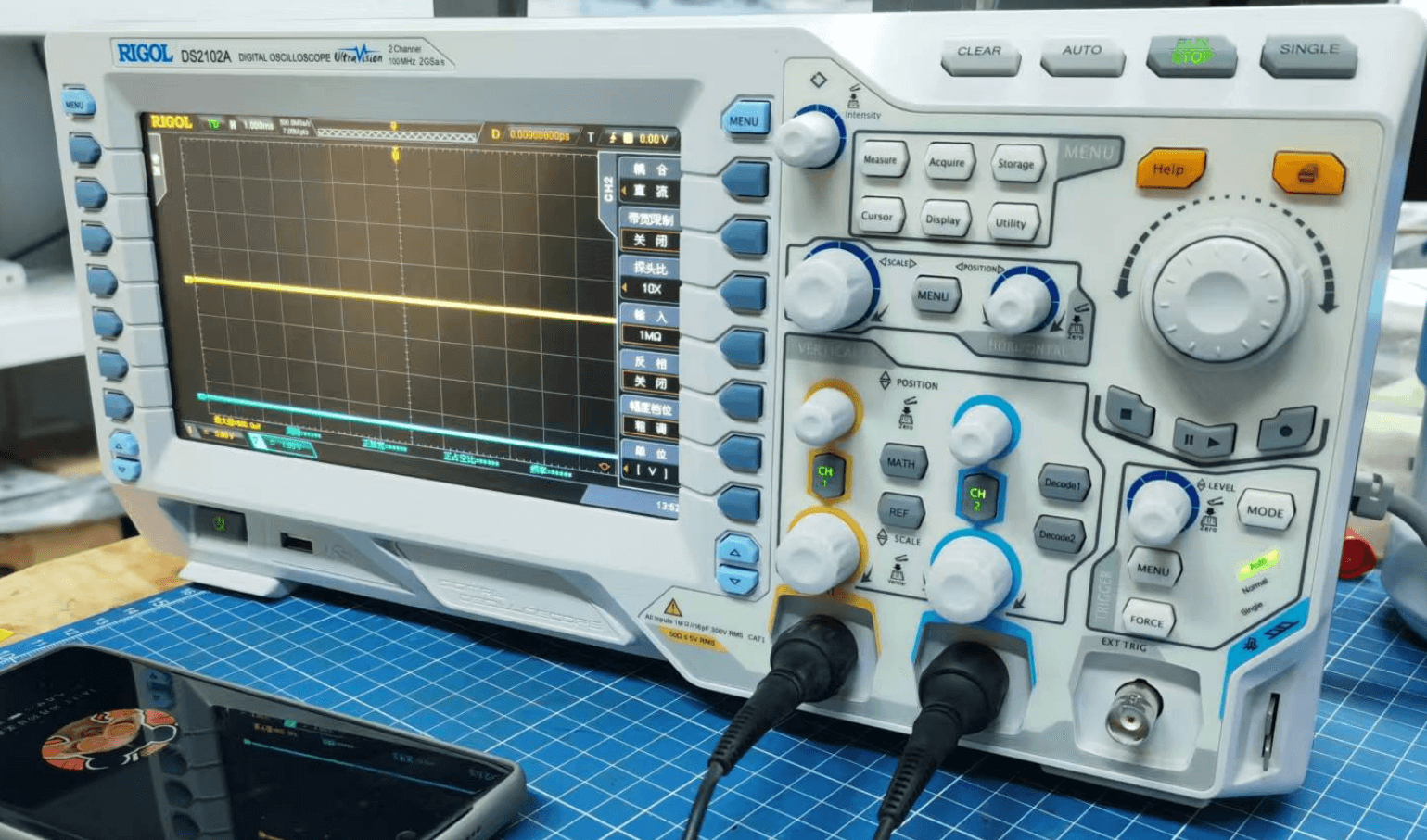
The specifications include below:
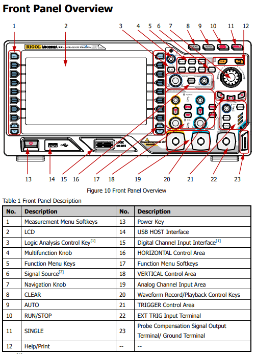
The user manual can be found here.
The key functions:
- Waveform Display: An oscilloscope can display the waveform of electronic signals in real-time. This allows you to visualize how the voltage varies over time.
- Signal Measurement It can measure various parameters of the signal, such as amplitude (voltage), frequency, period, rise time, fall time, and pulse width.
- Troubleshooting: Oscilloscopes are essential for diagnosing and troubleshooting problems in electronic circuits. They help identify issues like signal distortion, noise, and timing errors.
- Signal Analysis: Advanced oscilloscopes have features like FFT (Fast Fourier Transform) analysis, which allows you to analyze the frequency components of the signal.
- Triggering: Oscilloscopes have advanced triggering capabilities to capture specific events in the signal. This is useful for isolating and analyzing complex signals.
- Data Logging: Some oscilloscopes can log data over time, allowing you to monitor long-term trends and behavior in electronic systems.
- Protocol Analysis: Modern oscilloscopes can decode and analyze communication protocols (e.g., I2C, SPI, UART) used in digital systems.
Test using Ardiuno Uno with an ultrasonic sensor input (Oscilloscope)
First we need to connect the ultrasonic sensor to our Ardiuno board. The ultrasonic sensor's trig pin is connected to Arduino pin 2, the echo pin is connected to Arduino pin 3, and it is powered by connecting the GND and VCC pins to the Arduino's GND and 5V, respectively. Then the code for testing was uploaded as below. This code essentially triggers the ultrasonic sensor to send out an ultrasonic pulse, and the echo pin would later be used to measure the time it takes for the pulse to return, which can be used to calculate the distance to an object.
const int trigPin = 2;
const int echoPin = 3;

void setup() {
  pinMode(trigPin, OUTPUT);
  pinMode(echoPin, INPUT);
  digitalWrite(trigPin, LOW); // Ensure the trigPin is low at the start
}

void loop() {
  digitalWrite(trigPin, HIGH); // Send a HIGH signal to the trigPin
  delayMicroseconds(10); // Maintain the HIGH signal for 10 microseconds
  digitalWrite(trigPin, LOW); // Set the trigPin back to LOW
  delay(100); // Wait for 100 milliseconds before repeating the loop
}
To measure the waveform of the ultrasonic sensor's signal using an oscilloscope, follow these steps:
- Connect the Ground: Connect the oscilloscope's ground (GND) probe to the Arduino's ground (GND).
- Connect the Trigger Signal: Connect the oscilloscope's probe to the trig pin (pin 2 on the Arduino) to observe the trigger signal.
- Connect the Echo Signal: Connect the oscilloscope's second probe (if available) to the echo pin (pin 3 on the Arduino) to observe the echo signal.
The oscilloscope in the image below has key settings configured for measurement: the vertical scale for Channel 1 & 2 is set to 5 volts per division (5 V/div), and the timebase (horizontal scale) is set to 1 microsecond per division (1 µs/div), indicating how the waveform is represented on the screen.

The video for measurement shows the result. We can see that the echo signal length change with hand movement.
Test using XIAO-ESP32C3 with an LED output (using Multimeter)
To understand the current draw of a XIAO-ESP32C3 when driving an LED, you can use a multimeter in ammeter mode to measure the current consumption in the circuit. Here's how:
Materials Needed:
- XIAO-ESP32C3 development board
- LED (e.g., standard 5mm red LED)
- Resistor (e.g., 220Ω current limiting resistor)
- Breadboard and jumper wires
- Digital multimeter
Circuit Setup:
- Connect the LED’s anode (long leg) to a GPIO pin on the XIAO-ESP32C3 (e.g., D8).
- Connect the LED’s cathode (short leg) to one end of the resistor.
- Connect the other end of the resistor to GND.
- Power the XIAO-ESP32C3 via USB.
Multimeter Configuration:
- Turn the multimeter knob to the DC current (A or mA) setting.
- Remove the jumper wire between the power source and VCC pin, or between GPIO and LED, depending on whether you want to measure total board current or just the LED output.
- Insert the multimeter in series between the two disconnected points:
- For total current: between the power supply and VCC.
- For LED current only: between the GPIO pin and the LED anode.
LED Test Code
#define LED_PIN 8

void setup() {
  pinMode(LED_PIN, OUTPUT);
}

void loop() {
  digitalWrite(LED_PIN, HIGH);
  delay(500);
  digitalWrite(LED_PIN, LOW);
  delay(500);
}
Observing the Readings
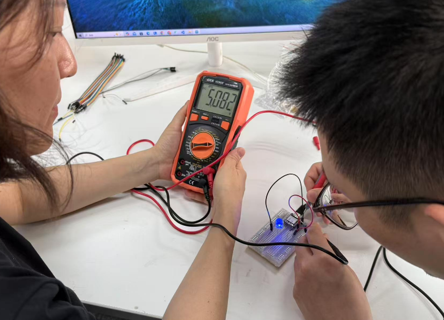
The overall voltage output is 5.08V.
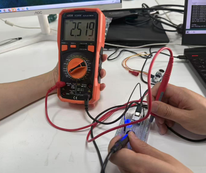
The overall current through the circuit is 2.51mA.
PCB Design
What is PCB
A PCB (Printed Circuit Board) is a flat board made of insulating material that holds and connects electronic components through conductive pathways. It serves as the backbone for most electronic devices, providing mechanical support and electrical connections for components such as resistors, capacitors, and integrated circuits.
- Key Features of PCBs:
- Material: Typically made from fiberglass, epoxy, or other insulating materials, with copper layers for the conductive pathways.
- Layers: Can be single-layer, double-layer, or multi-layer, depending on the complexity of the circuit.
- Components: Components are soldered onto the PCB, which provides both physical support and electrical connectivity.
- Design: PCBs are designed using specialized software, which allows for the layout of components and routing of electrical connections.
Software:Fusion 360
Fusion 360 is a cloud-based 3D CAD, CAM, and CAE tool developed by Autodesk. While primarily known for mechanical design and engineering, it also includes features for designing PCBs (Printed Circuit Boards). Fusion 360
- Key Features for PCB Design in Fusion 360:
- Integrated Workflow: Fusion 360 allows seamless integration of electronic design with mechanical design. You can design the PCB and its enclosure within the same environment.
- Schematic Capture: Users can create and edit schematic diagrams, defining the electrical connections and components in the circuit.
- PCB Layout: Fusion 360 provides tools to lay out the PCB, including placing components, routing traces, and managing layers.
- Design Rule Checks (DRC): The software can perform design rule checks to ensure that the layout meets electrical and manufacturing requirements.
- 3D Visualization: Fusion 360 allows you to visualize the PCB in 3D, helping to ensure that components fit properly within the overall design, especially when integrating with mechanical parts.
- Collaboration: Being cloud-based, Fusion 360 facilitates collaboration among team members, allowing multiple users to work on the same project simultaneously.
- Manufacturing Output: It can generate the necessary files for PCB fabrication, such as Gerber files, which are essential for manufacturing the PCB.
Other PCB Design software: EAGLE & KiCad
EAGLE (Autodesk EAGLE)
EAGLE is an electronic design automation (EDA) software developed by Autodesk. It provides a comprehensive suite of tools for designing printed circuit boards (PCBs).
Key Features:
- Schematic Capture: Create and manage schematics with ease.
- PCB Layout: Design PCB layouts with interactive routing and auto-routing options.
- Library Management: Access a vast library of components and create custom parts.
- 3D Viewer: Visualize your PCB design in 3D to check for mechanical fit.
- Integration: Seamlessly integrates with Autodesk Fusion for a unified design experience. EAGLE is available as part of an Autodesk Fusion subscription.
KiCad
KiCad is an open-source EDA software that provides a complete suite of tools for designing PCBs. It is free to use and runs on Windows, macOS, and Linux.
Key Features:
- Schematic Capture: Create schematics from simple to complex hierarchical designs.
- PCB Layout: Design PCB layouts with an interactive router and design rule check (DRC).
- 3D Viewer: Inspect your PCB design in 3D with a built-in raytracer.
- Library Management: Access a large library of components and create custom footprints.
- Community Support: Benefit from a vibrant community and extensive documentation. KiCad is a great choice if you're looking for a free and open-source solution for PCB design.
Microcontroller Unit(MCU) ESP32c3
Xiao ESP32-C3 is used in this design as MCU. See Intro. The Xiao ESP32-C3 is a compact and powerful development board designed for IoT (Internet of Things) applications. It features the ESP32-C3 chip, which is known for its performance, low power consumption, and integrated Wi-Fi and Bluetooth capabilities.
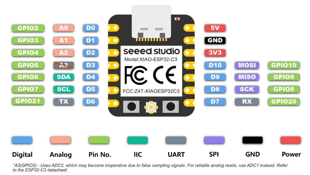
Key Features:
- Microcontroller: ESP32-C3, a 32-bit RISC-V single-core processor with a clock speed of up to 160 MHz.
- Wireless Connectivity: Wi-Fi: 802.11 b/g/n, supporting various modes and protocols for internet connectivity. & Bluetooth: BLE (Bluetooth Low Energy) for connecting to other Bluetooth devices.
- Memory: Typically includes 400 KB of RAM and 4 MB of flash memory for storing programs and data.
- GPIO Pins: Multiple GPIO pins available for connecting sensors, displays, and other peripherals, supporting various functions like PWM, I2C, SPI, and more.
- Compact Size: Small form factor, making it suitable for embedded applications and space-constrained projects.
- Low Power Consumption: Designed for energy-efficient operation, ideal for battery-powered devices.
Design with 360 Fusion
Create a PCB design with Fusion.
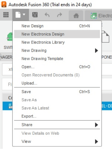
Download the PCB Design library at Link and import it your to your Fusion.
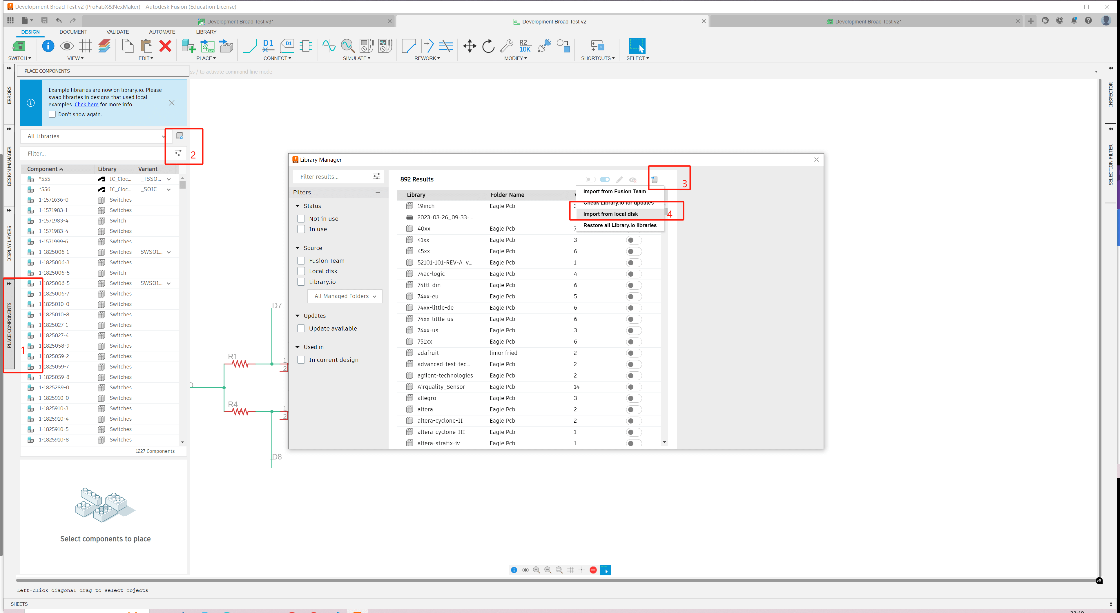
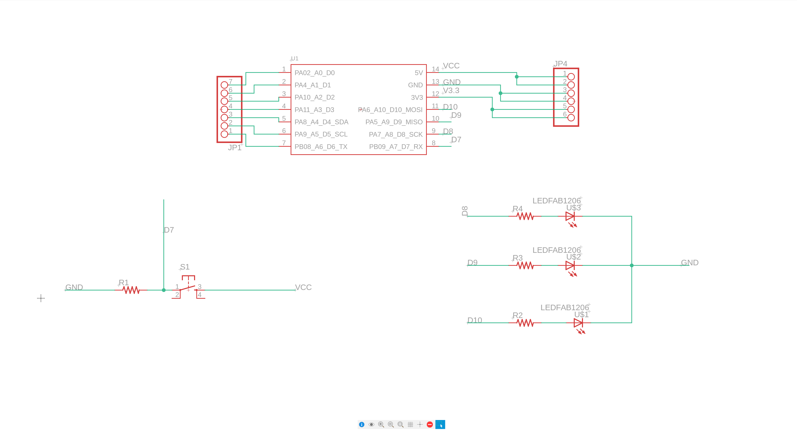
Add Dev-Board and Rename the Components, Supply and Other Electronics in schematics and draw the schematic diagram.
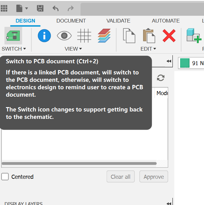
Switch into the Board View.
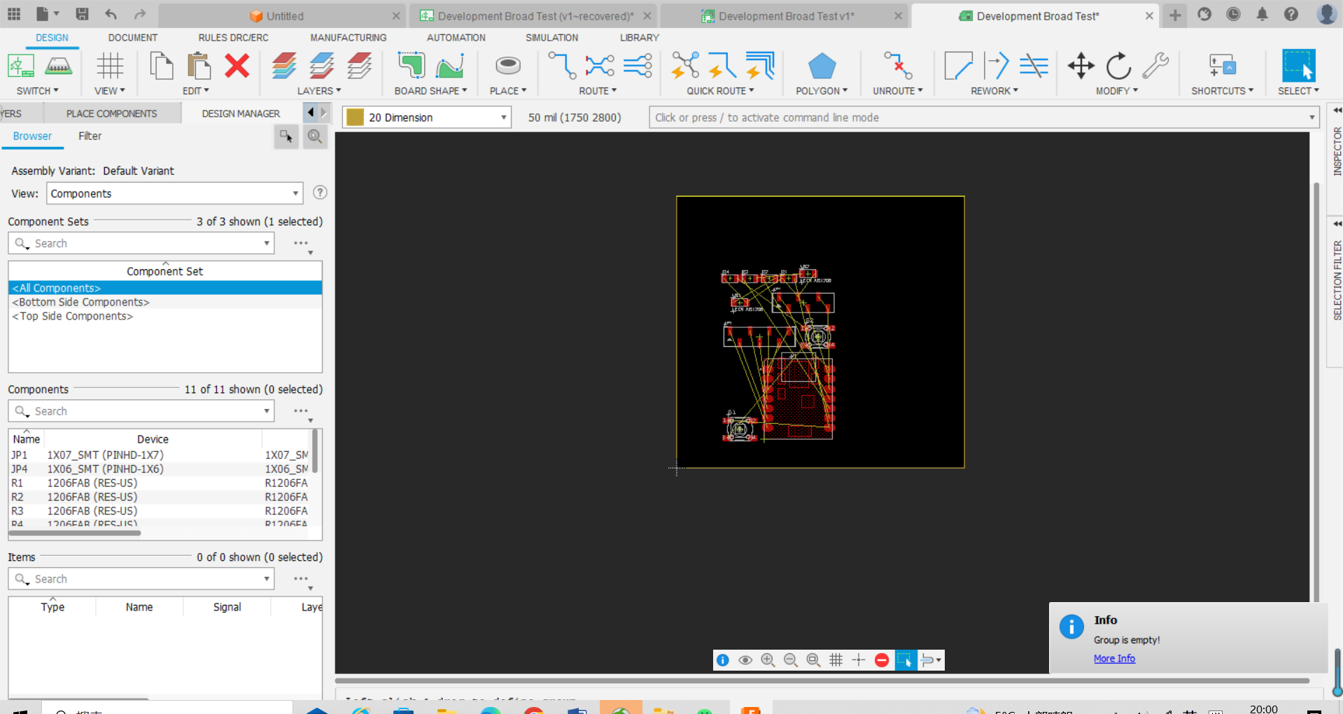
There are some design rules for PCB design. Click "Tool→DRC“ to set the clearance and sizes. DRC means "Design Rule Check", to make sure the circuit design can be manufactured by CNC. Traces and pads are not getting too closer and the traces width is wide enough to be cut out.
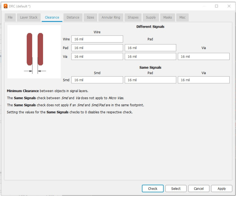
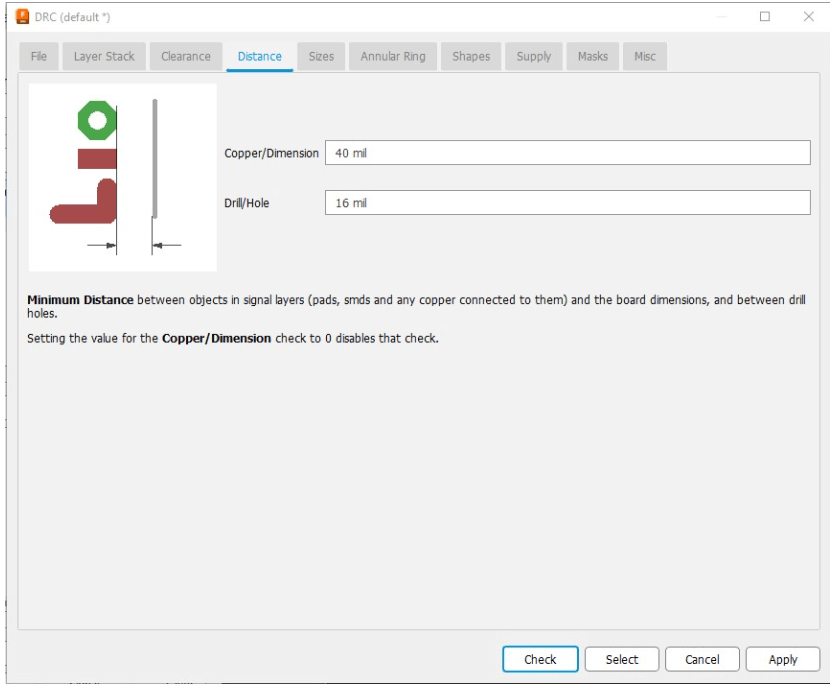
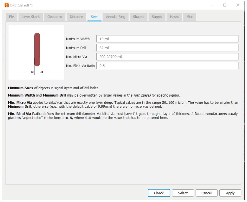
After DRC, manually place the component on the board and do a quick auto route.
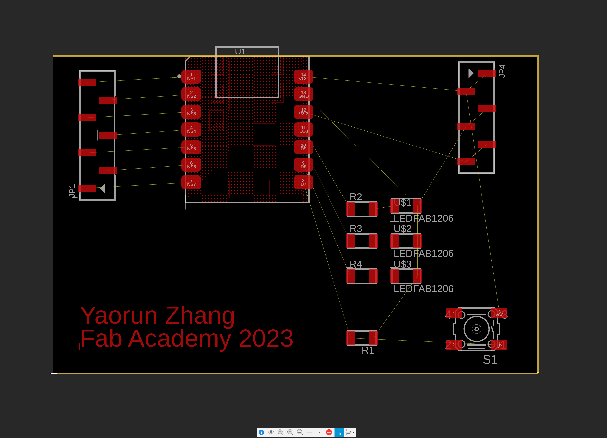
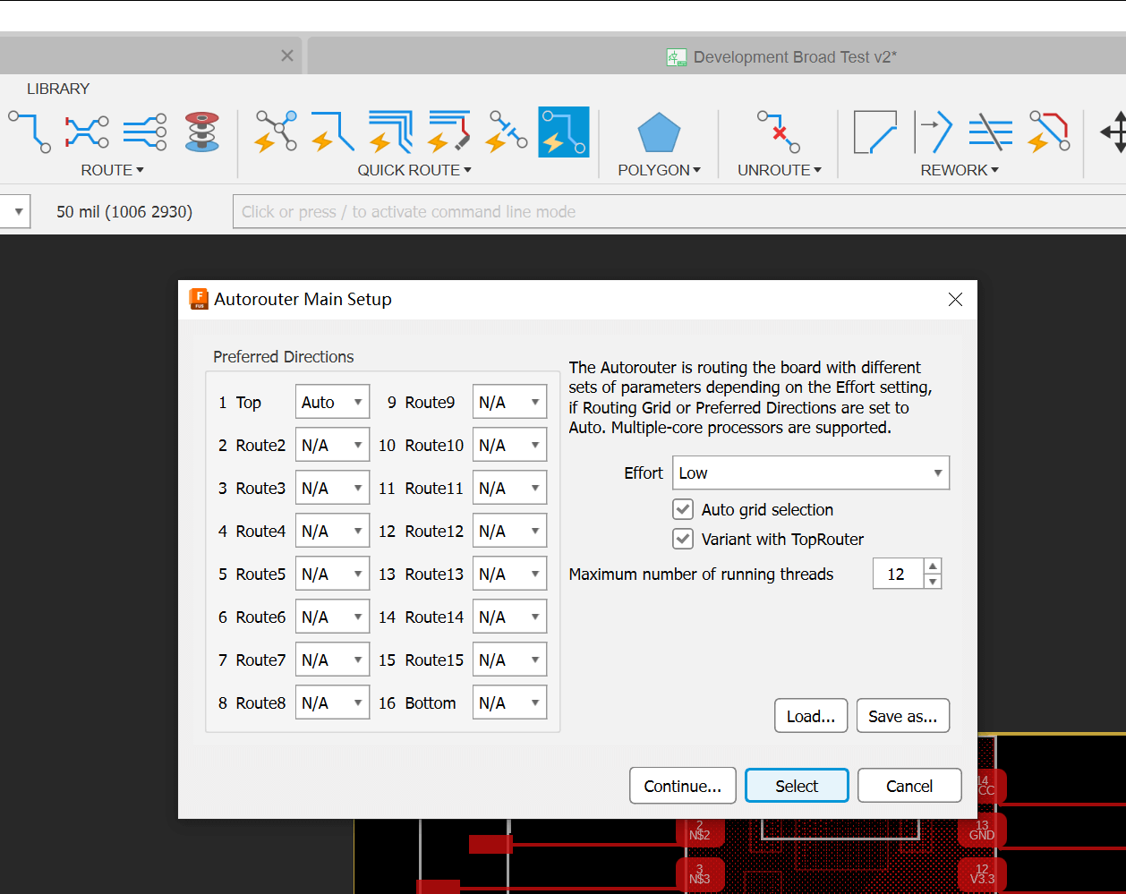
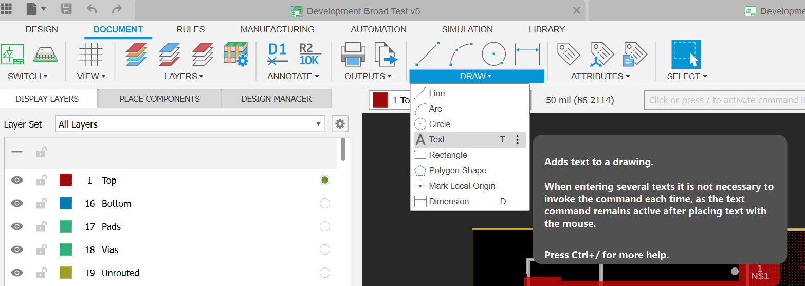
Manual adjustment of the Lines & Components, then add some text.
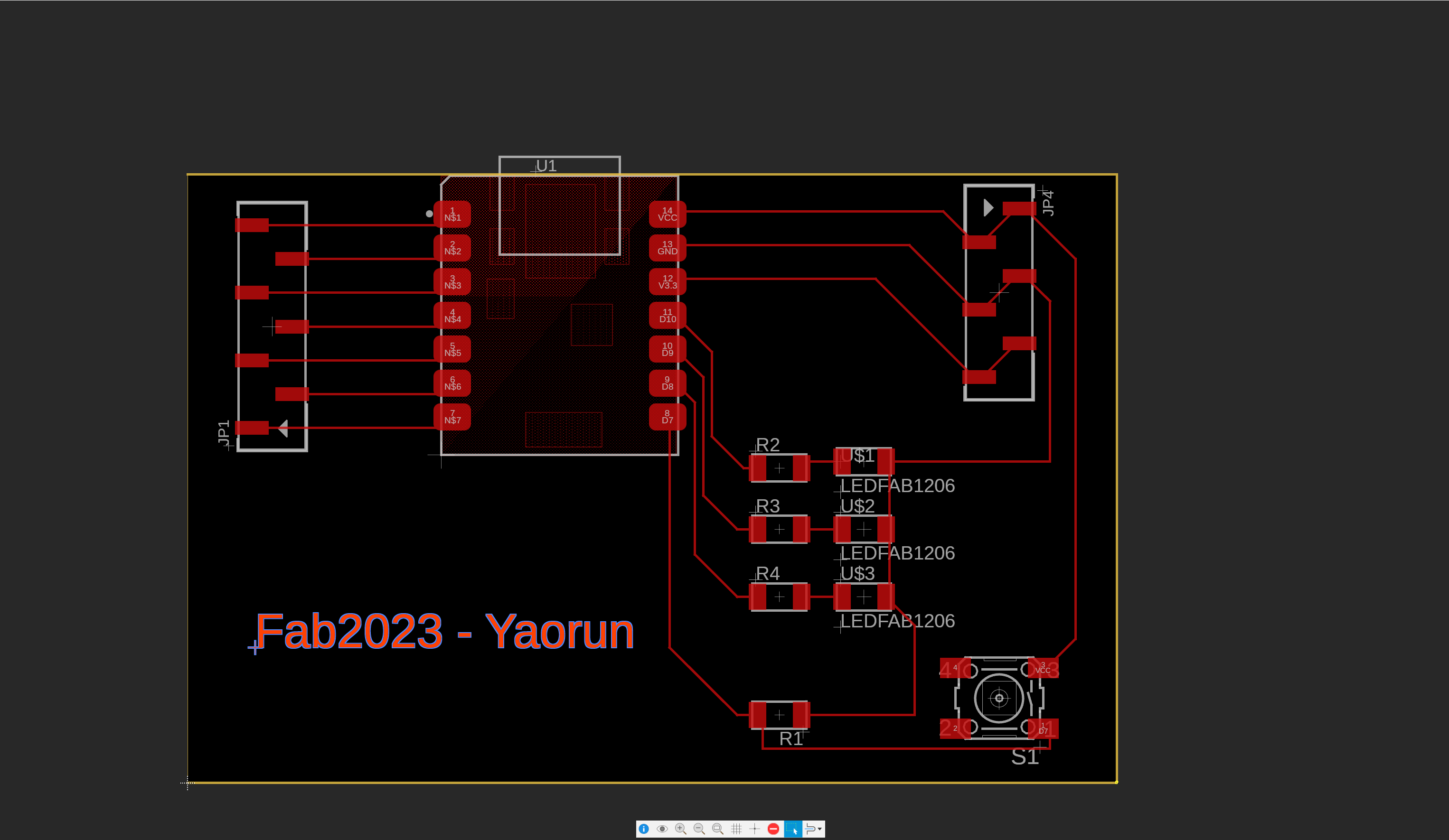
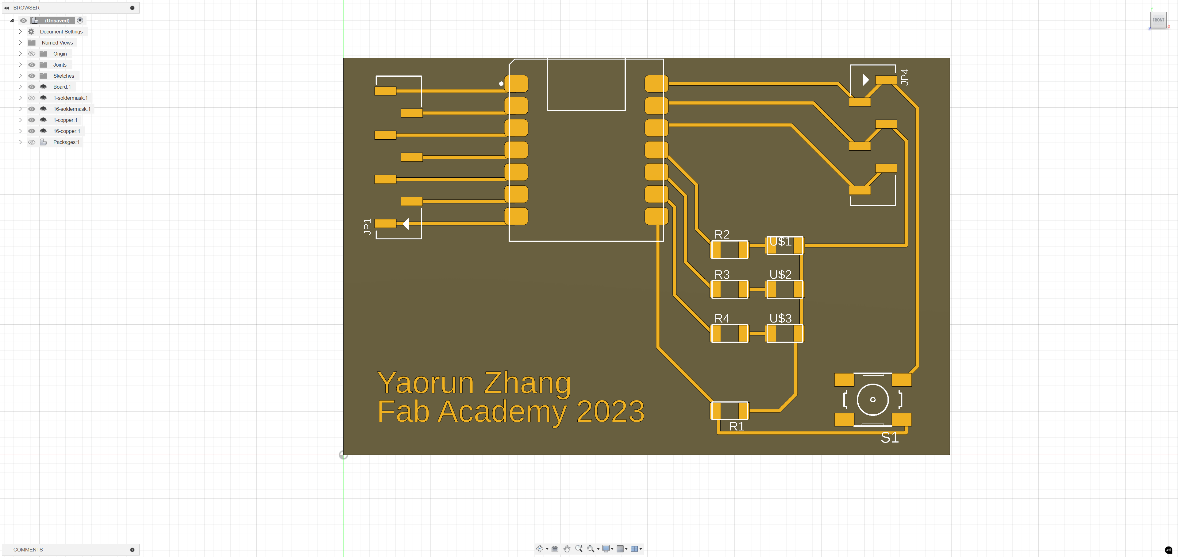
Push to 3D design see the result, I hide the mask layer & component in this output.
Reference
The PCB design can be downloaded via link here: https://a360.co/43Ta84H Or you can find the .step/.f3d file in my repo: https://gitlab.fabcloud.org/academany/fabacademy/2023/labs/ningbo/students/yaorun-zhang/-/tree/main/docs/assignments/week6?ref_type=heads