5. Electronics production
Task: Electronics Production
- Group assignment:(Page Link is Here)
- Characterize the design rules for your in-house PCB production process: document feeds, speeds, plunge rate, depth of cut (traces and outline) and tooling.
- document your work (in a group or individually)
- Document your work to the group work page and reflect on your individual page what you learned
- Individual assignment:
- Make an in-circuit programmer that includes a microcontroller by milling and stuffing the PCB, test it to verify that it works.
Electronics, I was always curious to that. I had purchase soldering irons two times. But I couldn’t complete most of projects, because, when I planed to make a electronic project. I faced 2 problems
- Lack of components in the stores in my town.
- Lack of guidance. I couldn’t even find a hobby circuit person in my connections
In this week, I can study pcb milling, soldering and program adding.
Our main aim in this week is to mill a pre-designed pcb, solder components and upload a program to that.
MODELA MDX-20
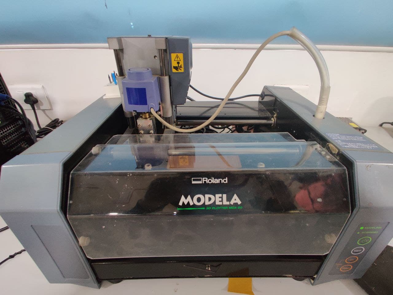
Roland Modela MDX-20 is used for many purposes in different industries.
Here we use the machine to mill the PCB.
Main parts of the Roland Modela MDX-20.
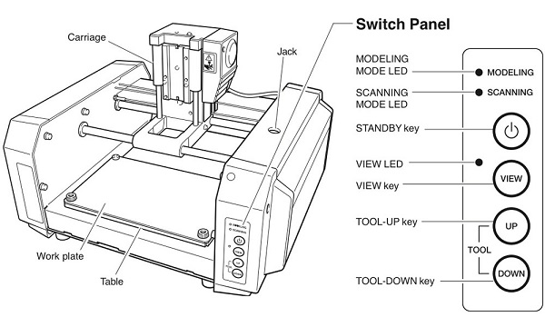
Axes
It is a 3 axes CNC machine. in which a cutting carrier moves in x and z direction and the work plate moves in the y-direction.
Cutting carrier
We can attach different bits to the cutting carrier. It moves in XZ plane. So it can engrave and cut with the same bit.
Work plate
We place the material for work on the work plate. It moves in the y-direction.
Switch panel
Modela MDX-20 has a basic switch panel which includes 4 switches.
Power button: It is for on and off
View button: When we click on the view button. The working bed will came towards the user.
Navigation keys: The 2 navigation keys are used for move cutting carrier up and down.
Configuring the Roland MDX-20
Before we begin milling, we have to set up the work plate and cutting carrier.
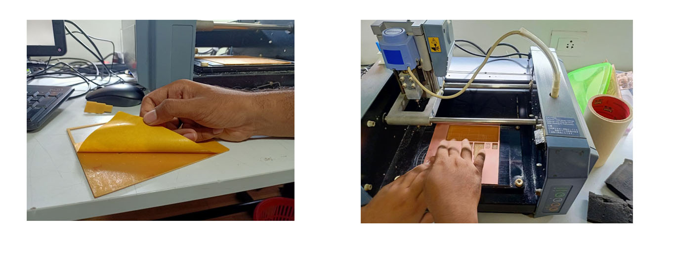
Setup the work plate.
We have to attach 2 layers of work materials to the work plate.
Our lab operators have already attached 2 sacrificial layers
It prevents the breakage of the bit during cutting of plate.
We paste the working material on the top sacrificial layer using a double-sided tape.
Setup the cutting carrier
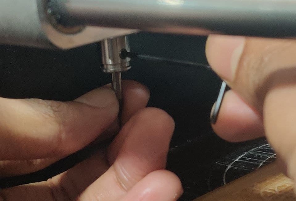
We have to insert/change the bit in to cutting carrier and to set the origin point.
Steps for changing bit.
- make sure the cutting carriage is on the top position.
-
Loose the 2 screws which are on two sides of the tool holding part using alen keys. We should support the tool using fingers to prevent the falling of the bit. Even it falls from a low height, the tip of the bit will break. Because the tip of the bits are very thin(1/64 and 1/32 inches)
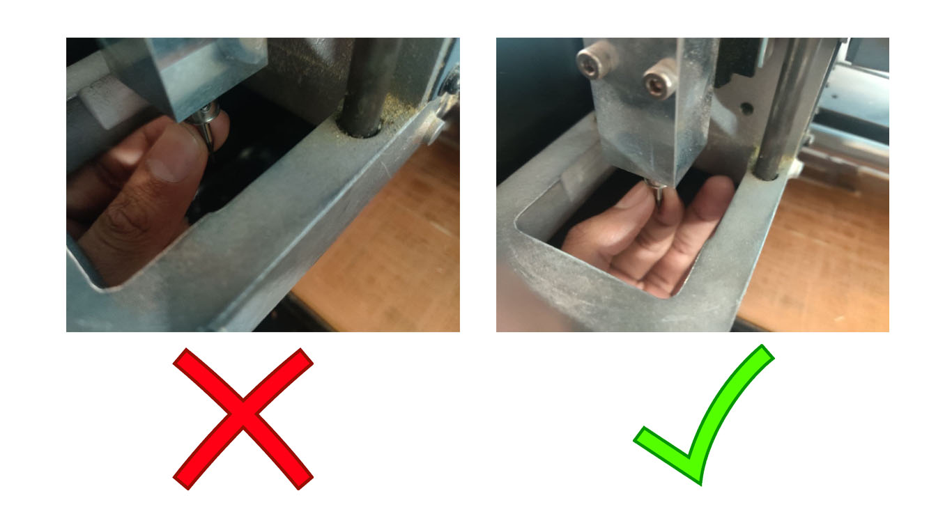
-
After getting the bit, place another bit to the bit holding hole and tighten 2 screws. We will ensure to pull the bit up to the parts above the cone shape is inside the bit holder.
-
Using up and down navigation keys, move down the cutting carrier and leave a 3-4 mm gap in between the working material and tip of the bit.
- After that, we can set the origin point using navigation keys for X and Y direction in ‘mods’ which will describe later.
- Then loose 2 screws ones more and make touch the tip of the bit to work material and tighten screws. We can press the work material a little to ensure the bit is touch to work material.
Downloading file
For making the PCB, I used the trace file and cut file from gitlab.fabcloud.org/pub(Link here)

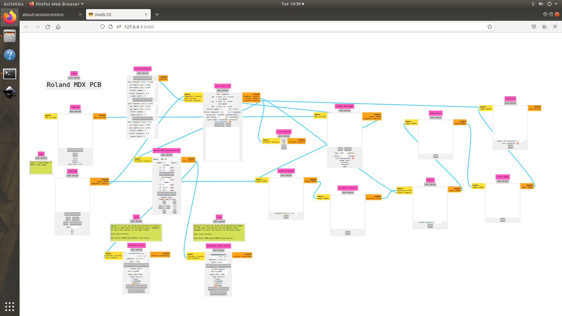
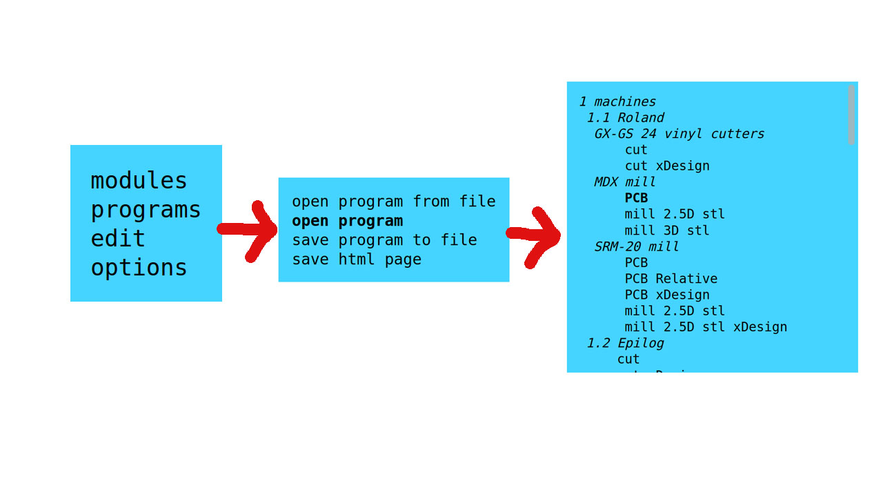
Using Mods
To send file and control other properties of MDX-20, we use Mods.
Steps are:
- Open Mods from the directory using the code below in terminal.
bash start-servers
-
Right click and follow as below. at last click on PCB under the MDX-20 option.
-
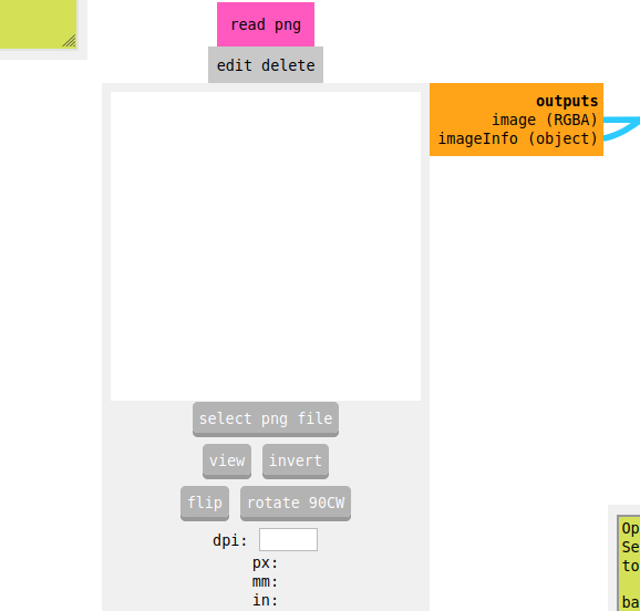
In the opening window, click on ‘add diagram’ button inside png option. and select the engraving diagram.
-
Select the bit from the ‘cutting tool’ option. For milling we use 1/64 inch bit. We can change the parameters if want.
-
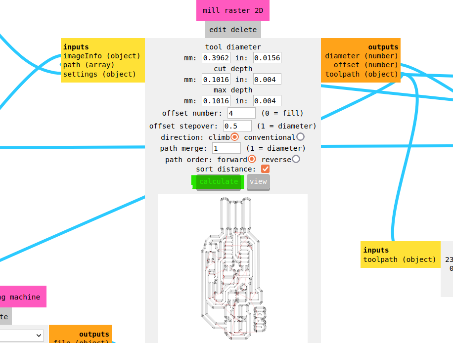
Click on calculate Butten under mill raster 2D. We can change the offset number, then the path for milling will show below.
-
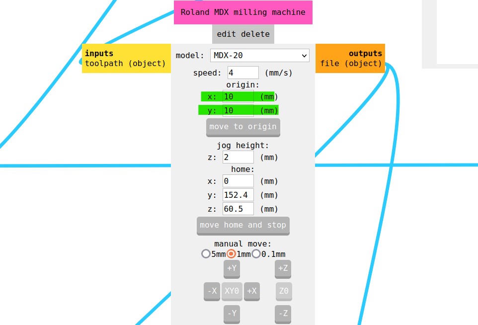
Set the origin point by typing different values for X and Y coordinates.
-
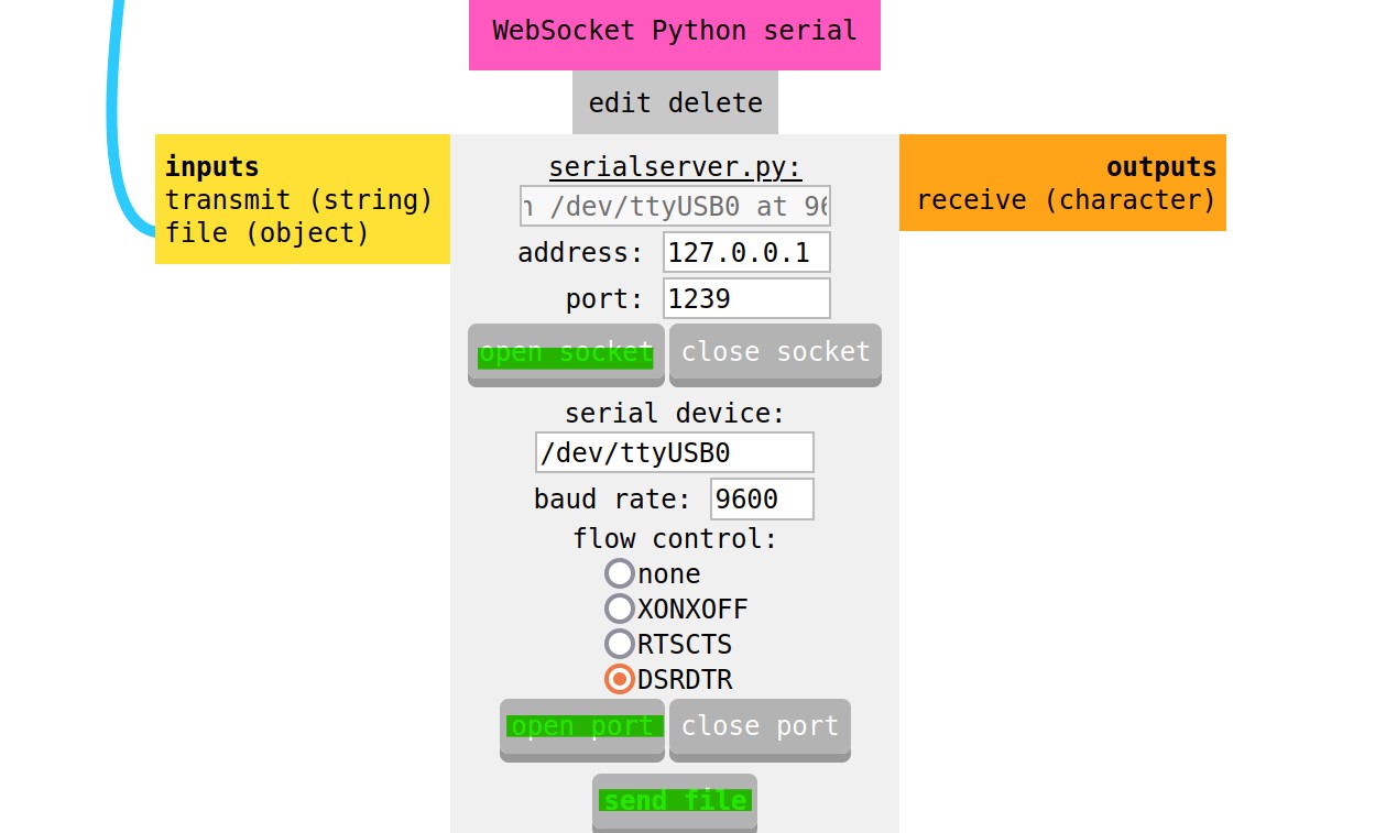
Click on ‘open socket’ and ‘open terminal’ and click on ‘send file’.
After the milling process, remove the dust using a vacuum cleaner.
Cutting.
We use a 1/32 inch bit for cutting.
Change the bit as described above section.
In Mods
upload the cutting diagram.
Select 1/32 bit.
Set origin point.
Click on ‘send file’ as described above.
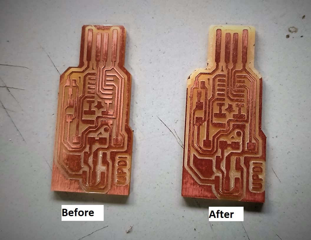
Polishing
After milling and cutting, Our PCB will have a rough surface. Polish the surface with san paper. And we have to remove the unwanted copper tracks in the edges.
Collecting different components.
Make a list of different components and collect those from fab academy inventory. And paste each parts near name of each component using a double-sided tape
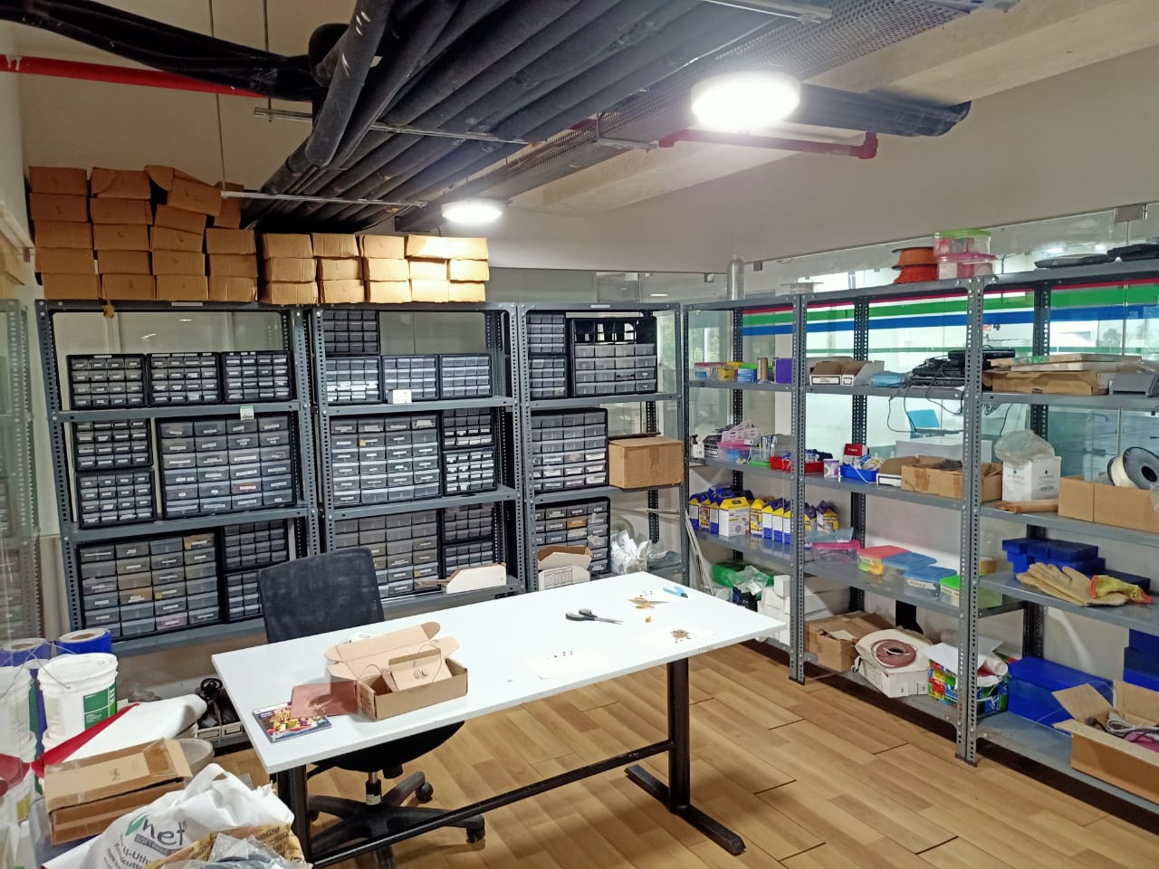
Inventory of Fab lab Kochi
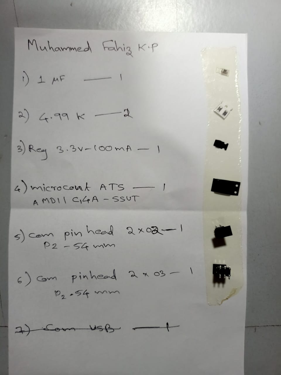
Components pasted on the list.
Soldering
Our mentor Gogin Francis introduced about soldering iron and soldering process. So I understood why my previous soldering became very bad.
How to solder better?
- Clean the surface and ensure there is no dust or oil particles.
- Set a temperature 350- 360 in soldeing iron.
- Apply a little paste on the soldering position.
- touch and the tip of the soldering iron in the soldering point by 45 degree angle and hold for 2 seconds.
- Then at the junction of soldering iron and surface, apply the led.
- After the the led melted and became in ball shape, take the soldering iron.
- When solder small SMD components, Use tweezer for pick and hold the components.
- When solder components with 3 or more legs, fix one leg in any corner and solder diagonal corner, and solder other legs.
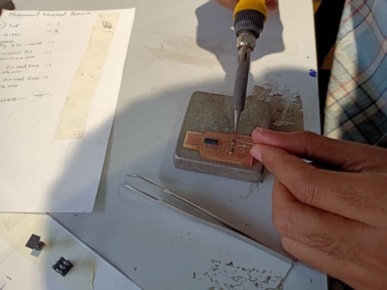
Soldering the board
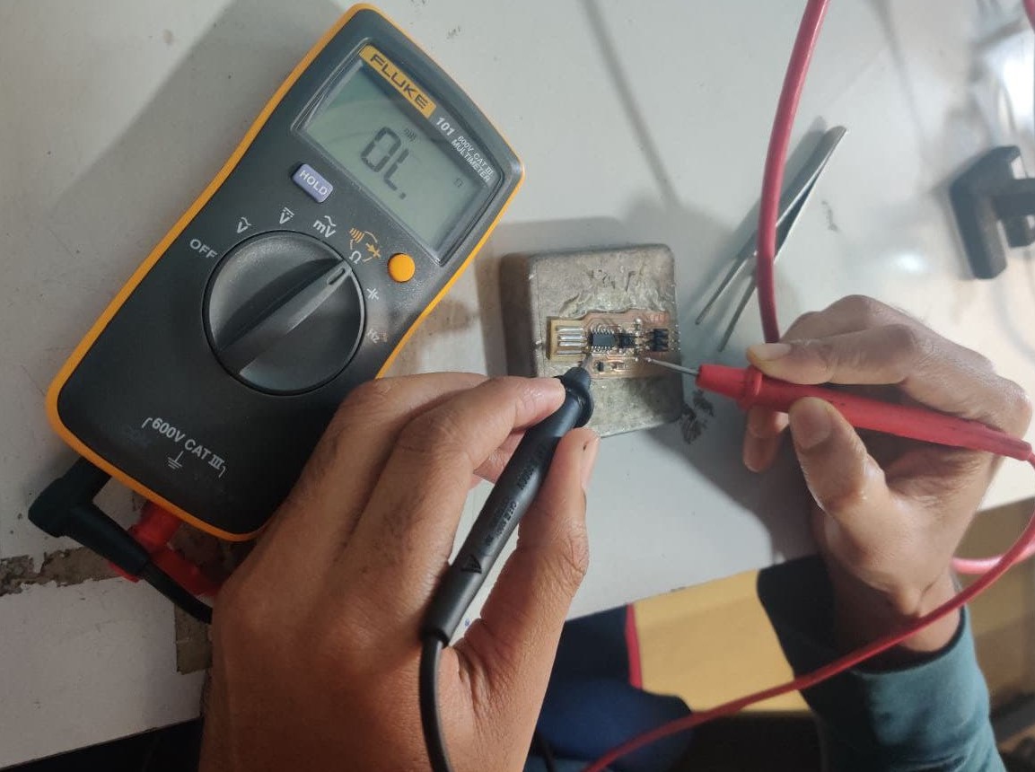
Checking connections in the PCB.
We have to check connections using multimeter before and after soldering process.
Before Soldering:
Check and ensure there are not any unwanted connections and each track are continues.
After soldering: Check and ensure there is not any short connection between adjecent pins of components and between adjecent tracks.
Programming
Download and install Arduino software.
Arduino software is open-source and we can simply download it from arduino.cc
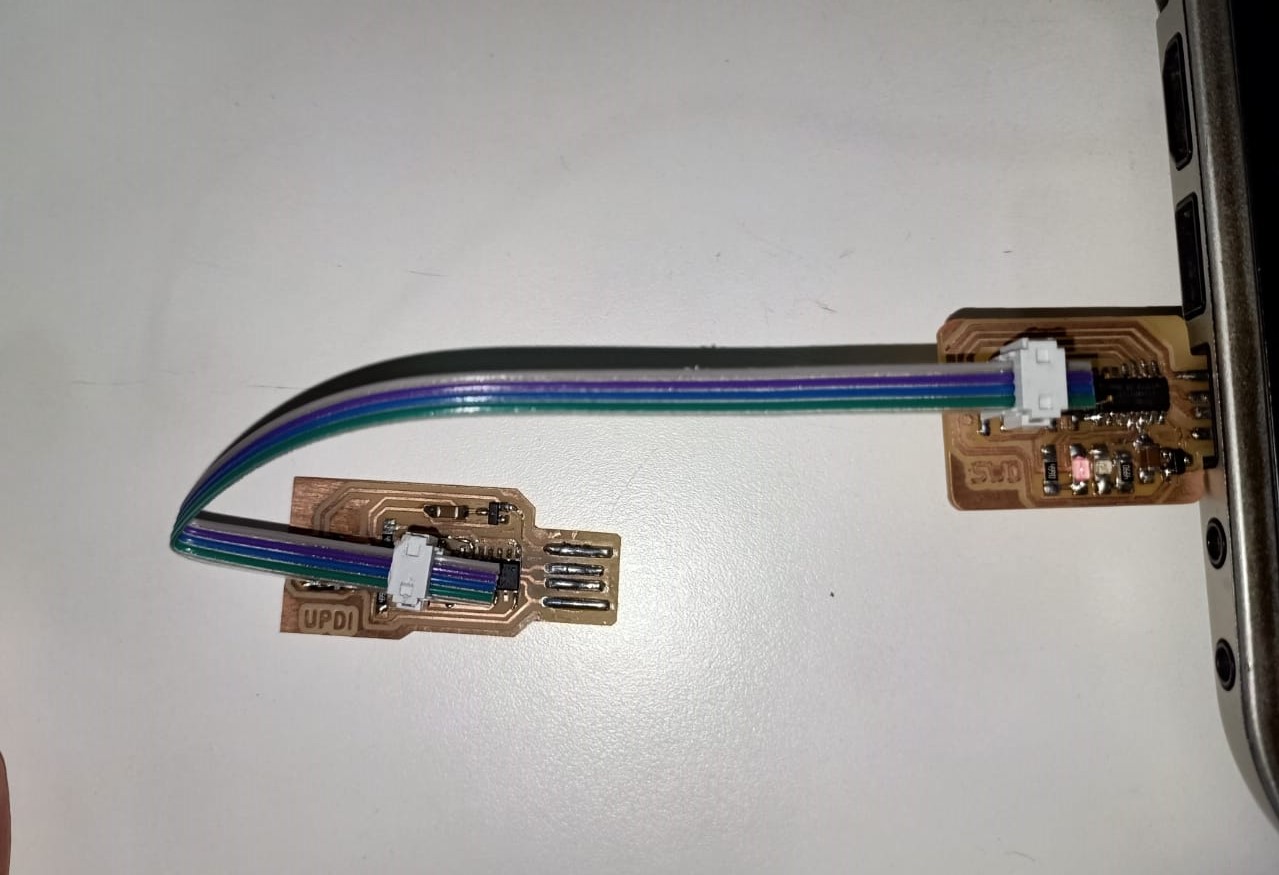
Burning bootloader
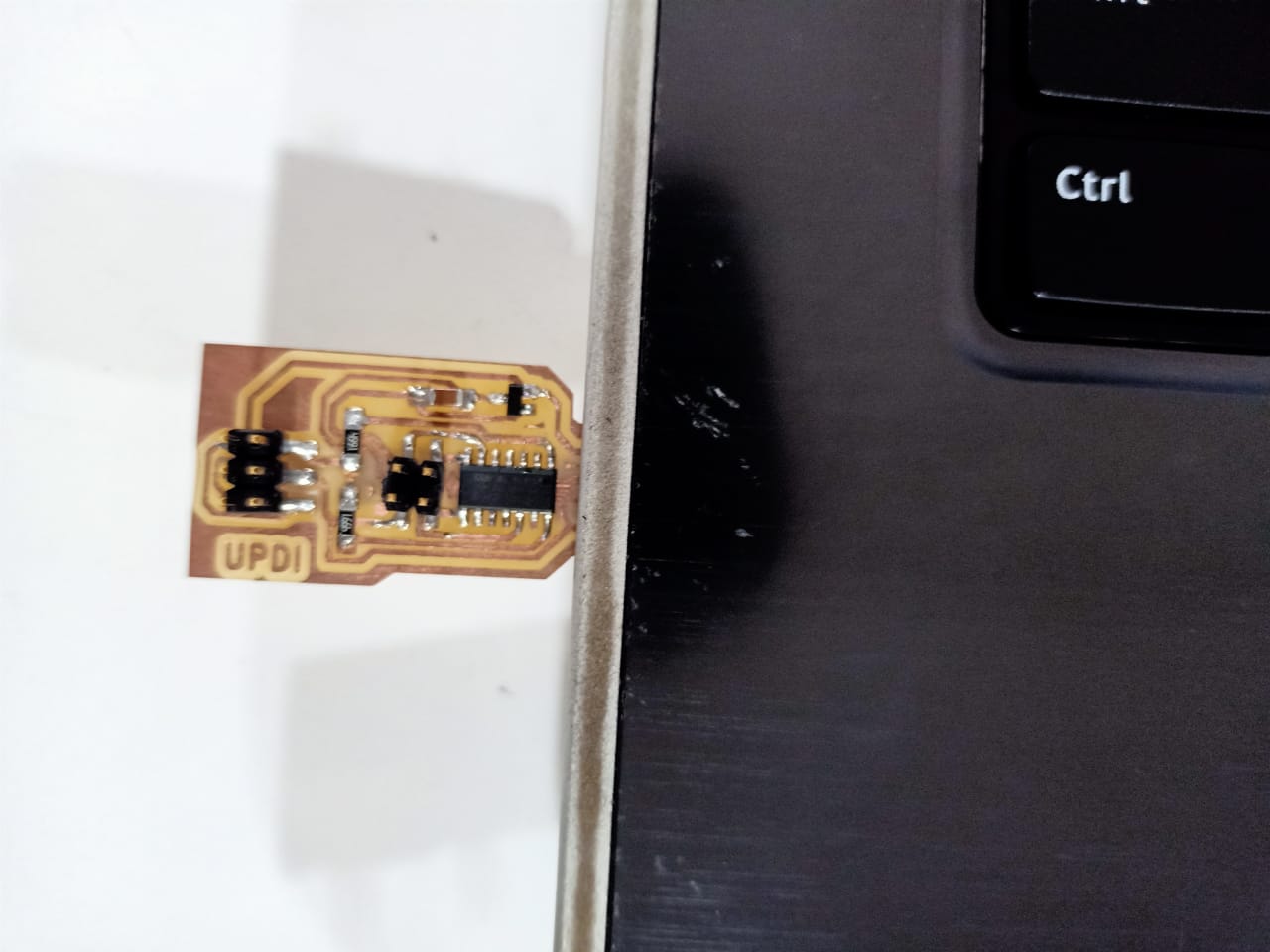
Now our microcontroller is blank. At first we have to upload a program to understand the usb communication protocol. For that here we used UPDI programmer with Atmel 546 microcontroller.
Steps
-
Plug Atme546 in a usb port and connect SAMD11C board using 2 pins.
-
Open Arduino software. and go to File → Preference and paste the code below.
[k](https://raw.githubusercontent.com/qbolsee/ArduinoCore-fab-sam/master/json/package_Fab_SAM_index.json)
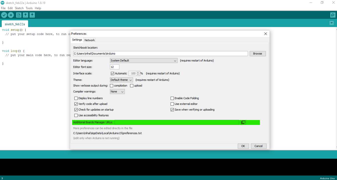 3. Go to Tool → Board → Board Manager and Search for Fab SAM core for Arduino and dowload that library.
4. Go to Tool→ Board→ Fab SAM core for Arduino and select Generic D11C14A
5. Go to Tools → Programmer and select Atmel EDBG
6. Go to Tools and click on Burn Bootloader
3. Go to Tool → Board → Board Manager and Search for Fab SAM core for Arduino and dowload that library.
4. Go to Tool→ Board→ Fab SAM core for Arduino and select Generic D11C14A
5. Go to Tools → Programmer and select Atmel EDBG
6. Go to Tools and click on Burn Bootloader

Now our board is ready to connect directly in USB port. We have to upload a program to that microcontroller
steps I followed are given below.
-
plug our board in a USB port.
-
Create a folder in computer and clone the files using following code in git.
git clone [https://github.com/qbolsee/SAMD11C_serial.git](https://github.com/qbolsee/SAMD11C_serial.git)
-
Open SAMD11C_serial.ino in Arduino software.
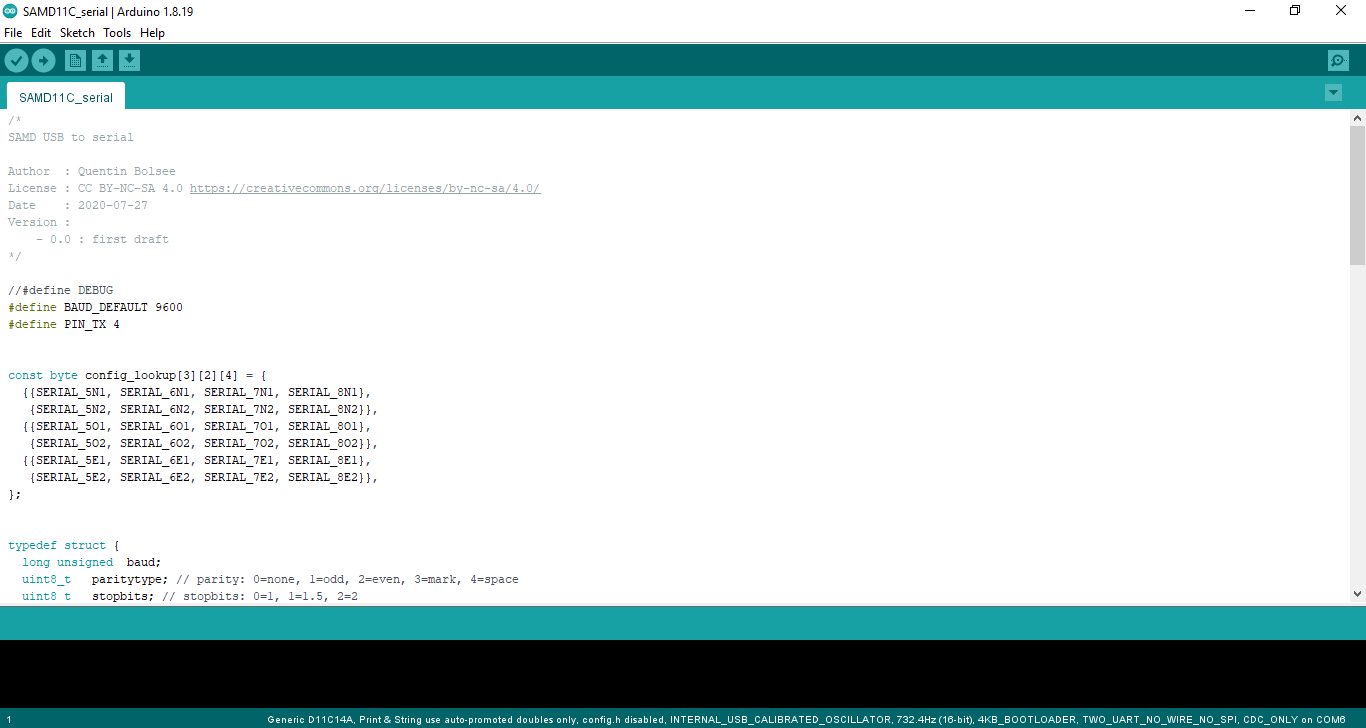
-
Go to Tool→ Board→ Fab SAM core for Arduino and select Generic D11C14A
- Go to Tools → port and select the USB port.
-
Click on verify and click on upload.
Now the board became programmed.
Study about drilling tools.
Our instructors Rahul and Gogin Francis explained us about different drilling tools and their properties.
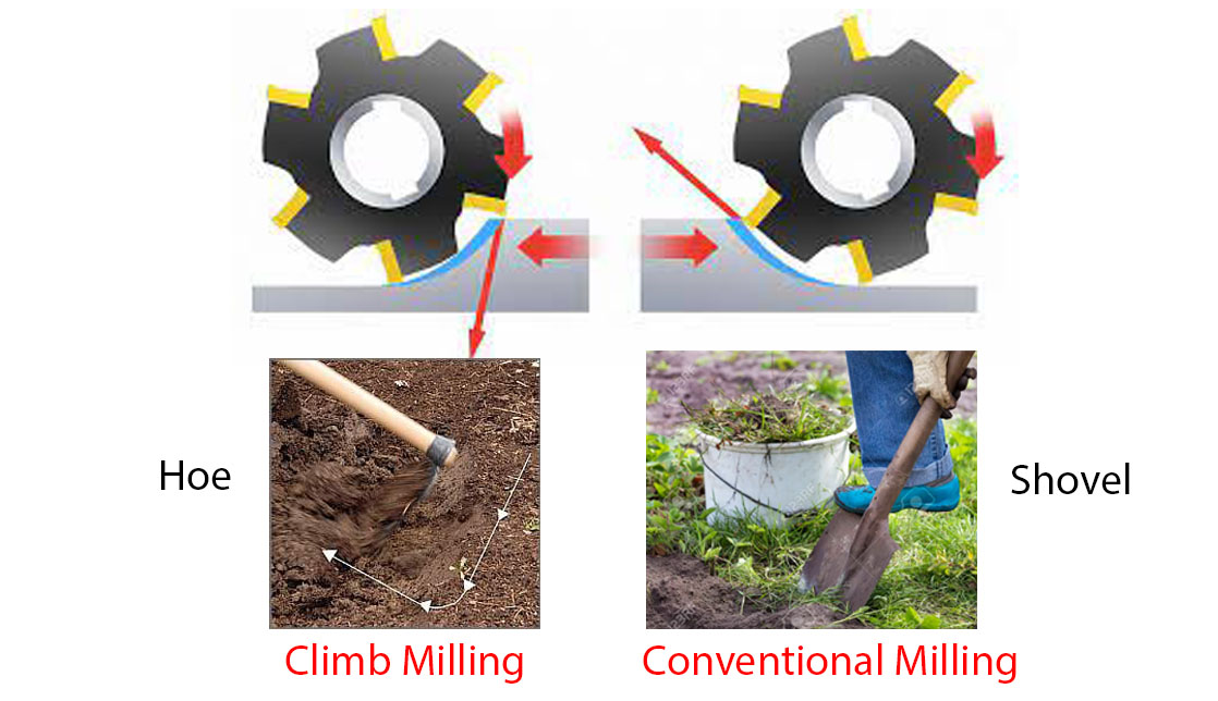
Climbing milling and Conventional milling
By comparing these to sow and shovel we could understand them very clearly.
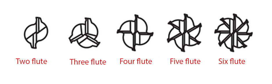
Flute number
If the number of flutes is increased, we must increase feed speed according to.
Single and two flute mills are used for high-speed machining and high-volume material removal like aluminum, plastic, etc.
Mils and Inch
Commonly bit diameter is represented in mills and inch.
1 Inch = 1000 Mils
1 mill = 0.001 Inch
1/32 Inch= 31.25 Mils ≈ 31 Mils
1/64 Inch= 15.625 Mils ≈ 16 Mils
We have to check the smallest thickness for gap and grooves in a pcb
In
64 bit
32 bit
100 bit
vinyl
In the milling process, we can compare increasing flute number into increasing
-
Load the material to be milled, add the tool for tracing, i.e. 1/64 inch mill and then set x, y and z axis.
-
Load the png file “linetest” you are going to trace from the download earlier.
-
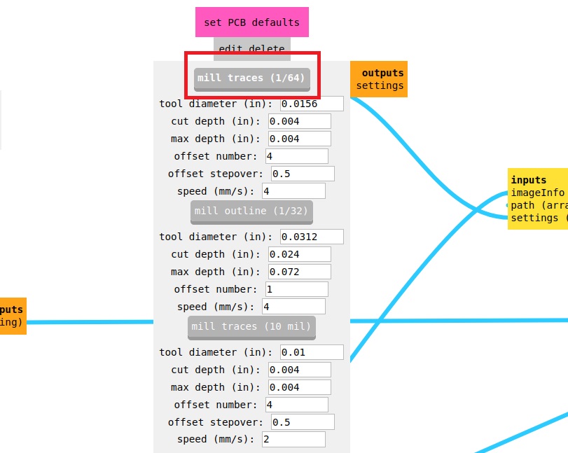
Set the tool to 1/64 inch mill, set offset at 4, stepover 0.5 and speed 4mm/s, hit calculate and then open socket, open port and send the file which should start the cut.
Group Assignment.
Aims of the Group Assignment.
- Find the small trace thickness during PCB milling using a specific bit.
- Find the smallest gap between 2 traces using a specific bit.
- Send a PCB out to a board house.
Line Test
We used bits of 1/64 inch, 1/32 inch and 1/100 inch.
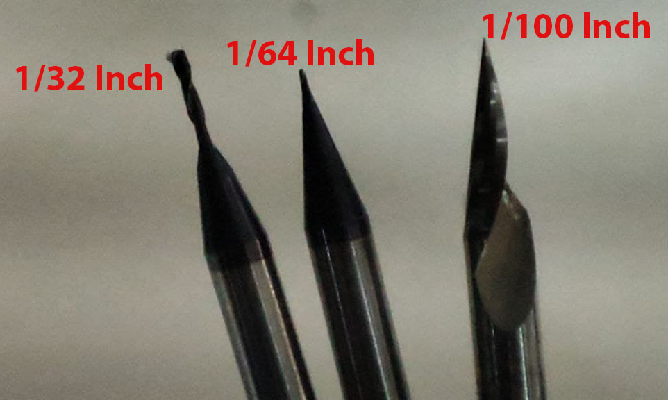
The png files are given by Fab academy.

We milled using different bits and cut the outline by 1/32 inch bit.
We used the preset settings for each bits.
Our outputs are given below.
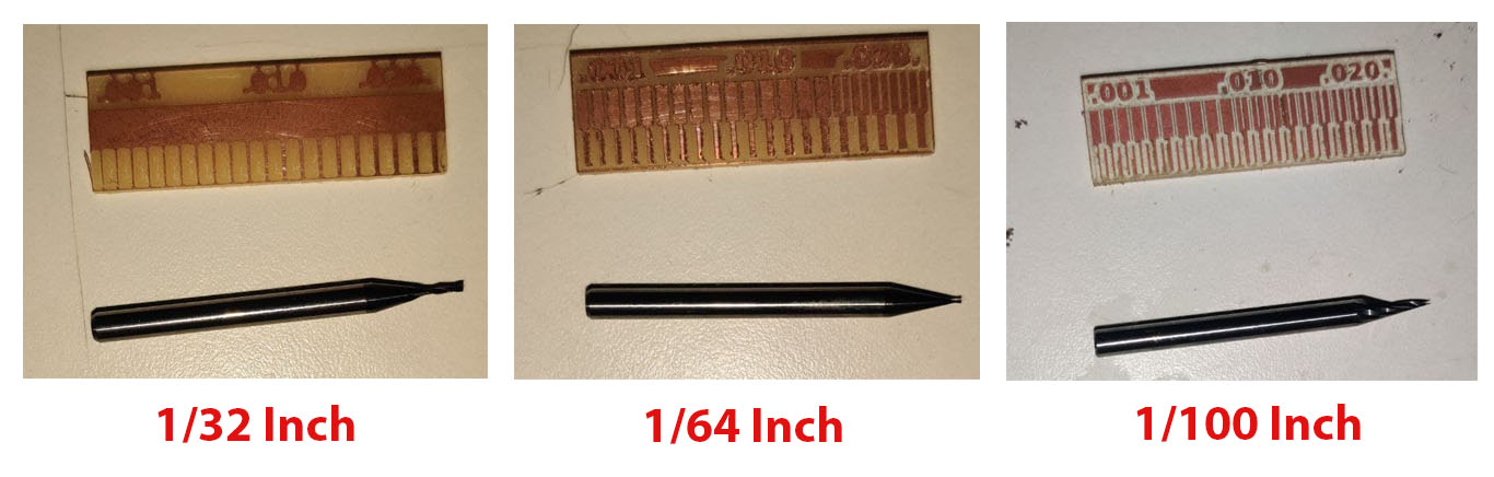
After the examination, we came to the conclusion that
- 1/64 bit can trace upto 0.16 mm
- 1/32 bit cannot be used to make traces, better to use as a cutting tool
- 1/10 bit can trace upto 0.11 mm