
Electronics Production
Individual Assignment:
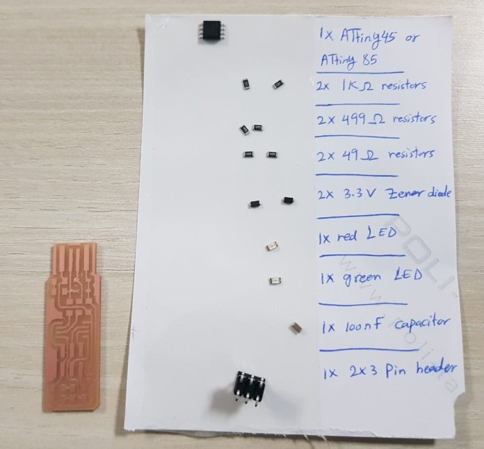
- Make an in-circuit programmer (Fab TinyISP) by milling and stuffing the PCB, test it, then optionally try other PCB fabrication process.
Group Assignment:
- To try milling by two different milling bits with different sizes to observe the difference in the results between them.
1. PCB Fabrication
Techniqe 1: PCB fabrication by using CNC Milling Machine
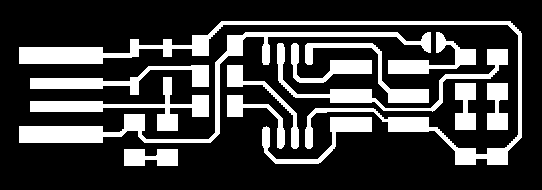
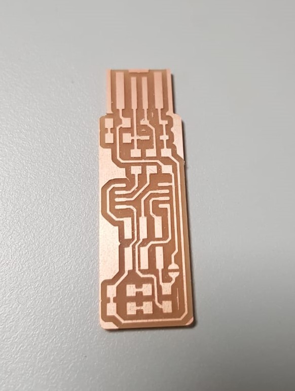
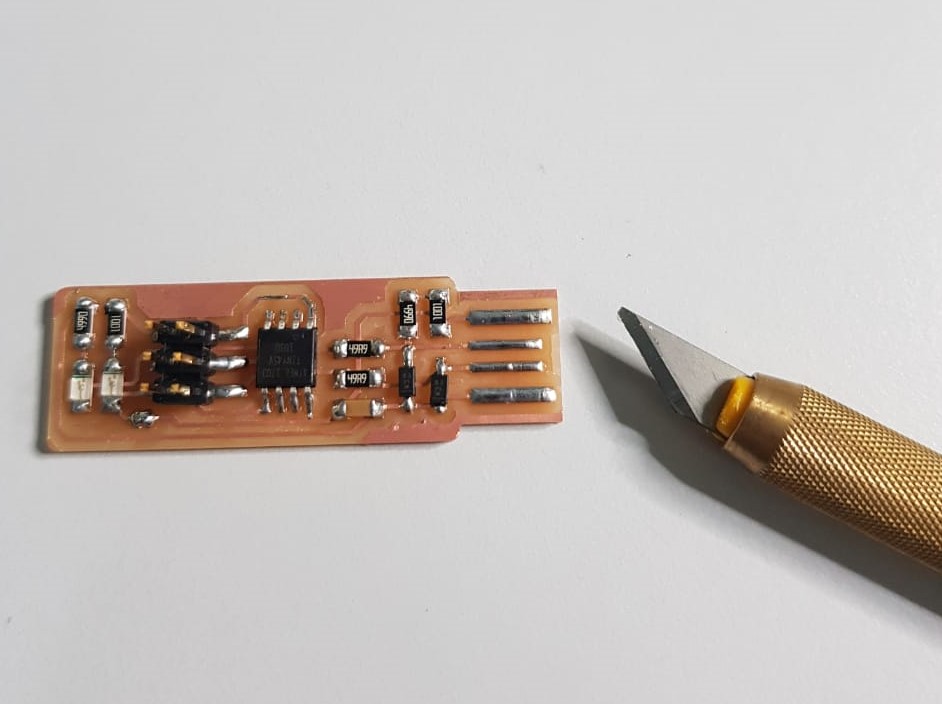
The first board I fabricate was the Fab TinyISP.
Fab TinyISP: is a programmer board that is used in programming other PCBs.
Click here for the reference link of FabTinyISP.
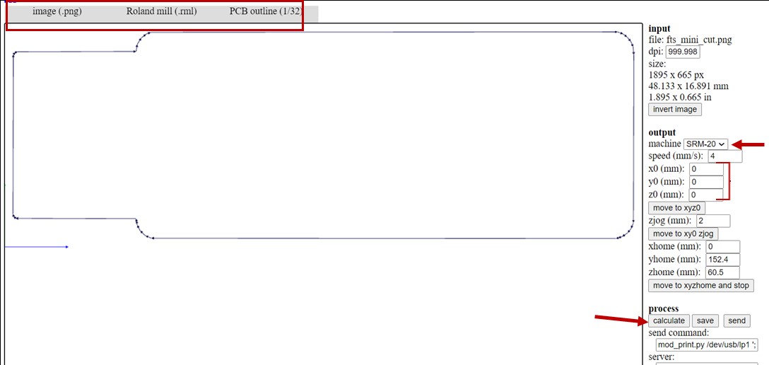
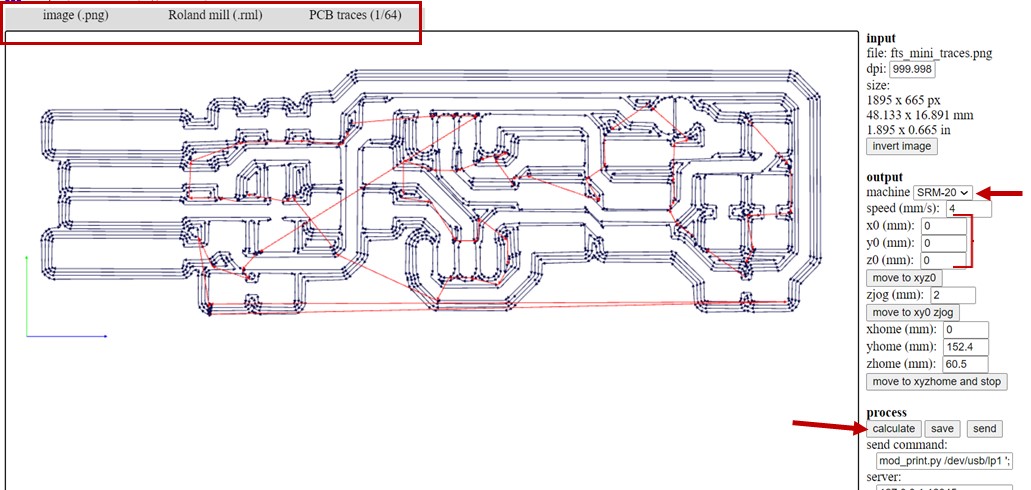
I used the following traces image and outline image of the Fab TinyISP
and I convert them into a format that the Milling machine understands by using Fab Modules website.

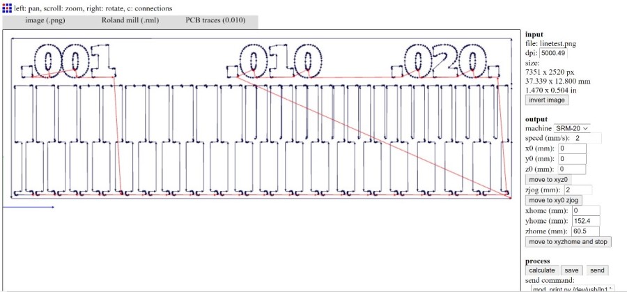
In Fab Modules, I went first to the top left and select the png image for the input and .rml for the output which is the format that the milling machine understand. Then I select PCB traces (1/64) for the traces image and PCB outline (1/32) for the cutout outline image. After that I choose the name of the machine which is SRM-20 and I put the x, y and z axis to zero and finally calculate. The lines shown in the picture are the paths that the milling machine will move on to engrave the copper board.
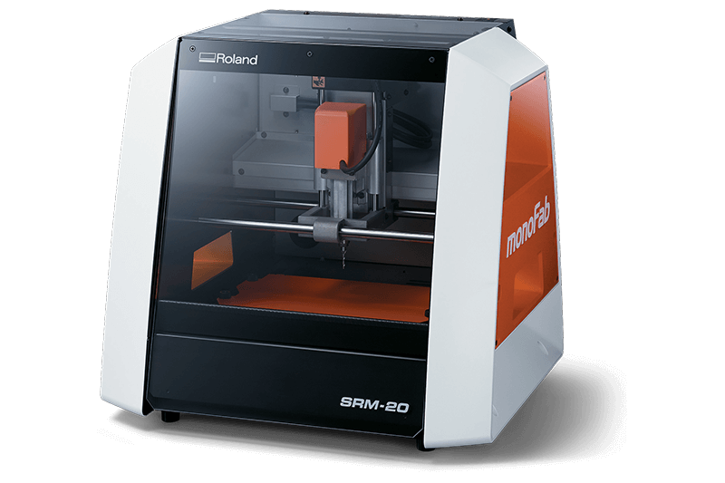
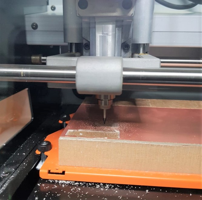
Then I took these two .rml files to the Milling machine. This is the Roland CNC Milling machine I used in the lab.
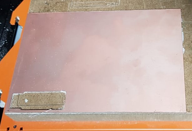
And before starting milling, I took a copper board which is shown in the below picture and put it in the machine then I set the origin position
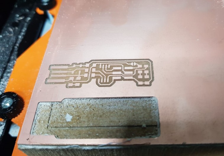
And this is the production of the milling machine
Then I started collecting all the components I need to solder
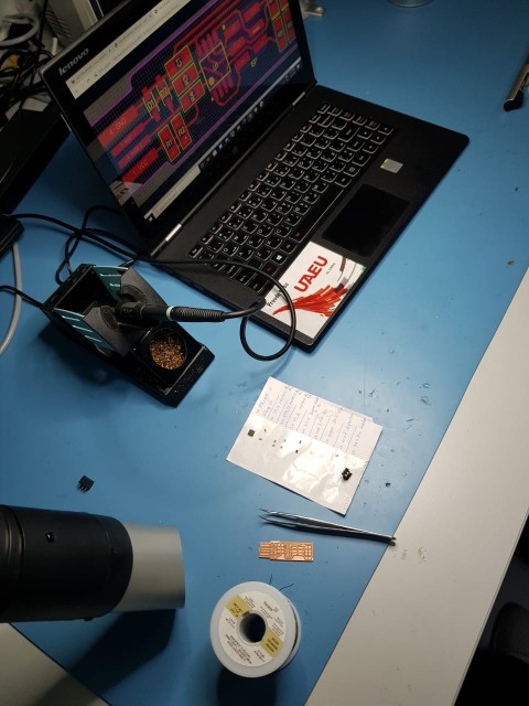
Here I started solding
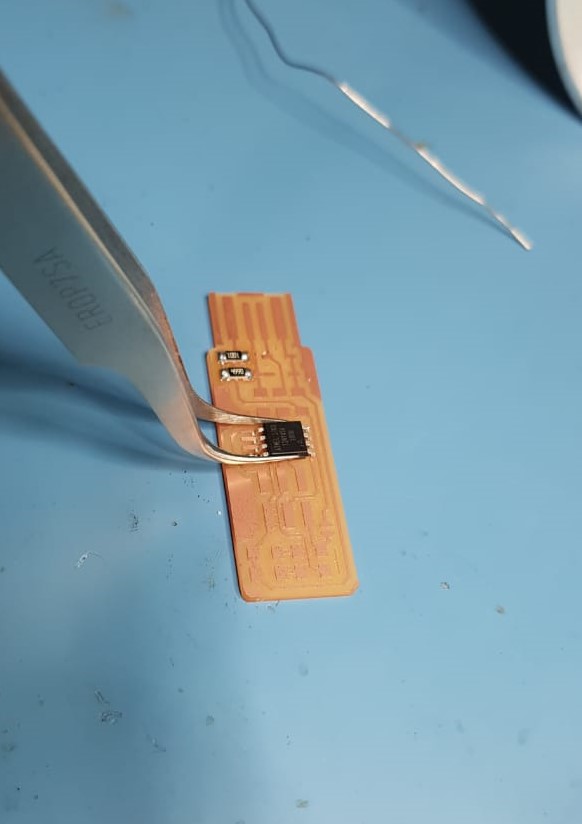
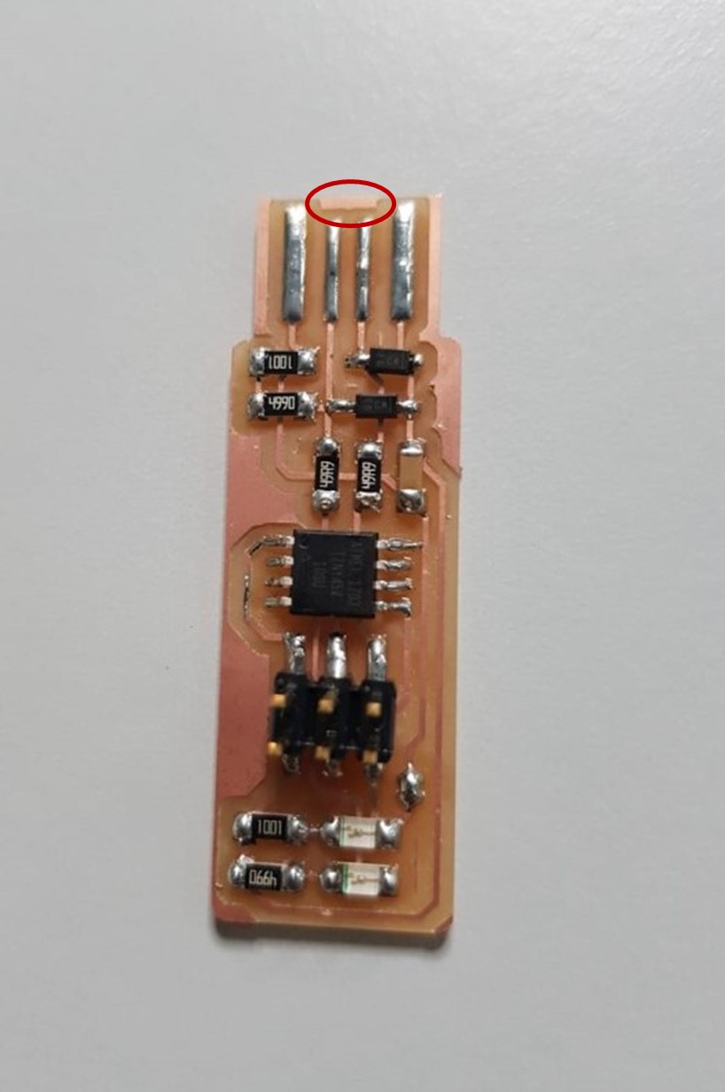
And here I'm done with soldering. After that, I removed the copper shown in the image to ensure there will be no short circuit while inserting the ISP in the laptope.
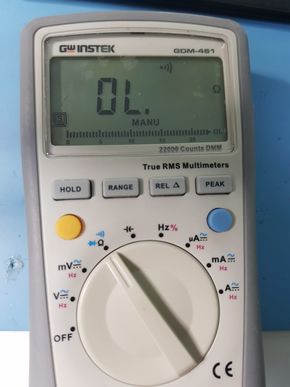
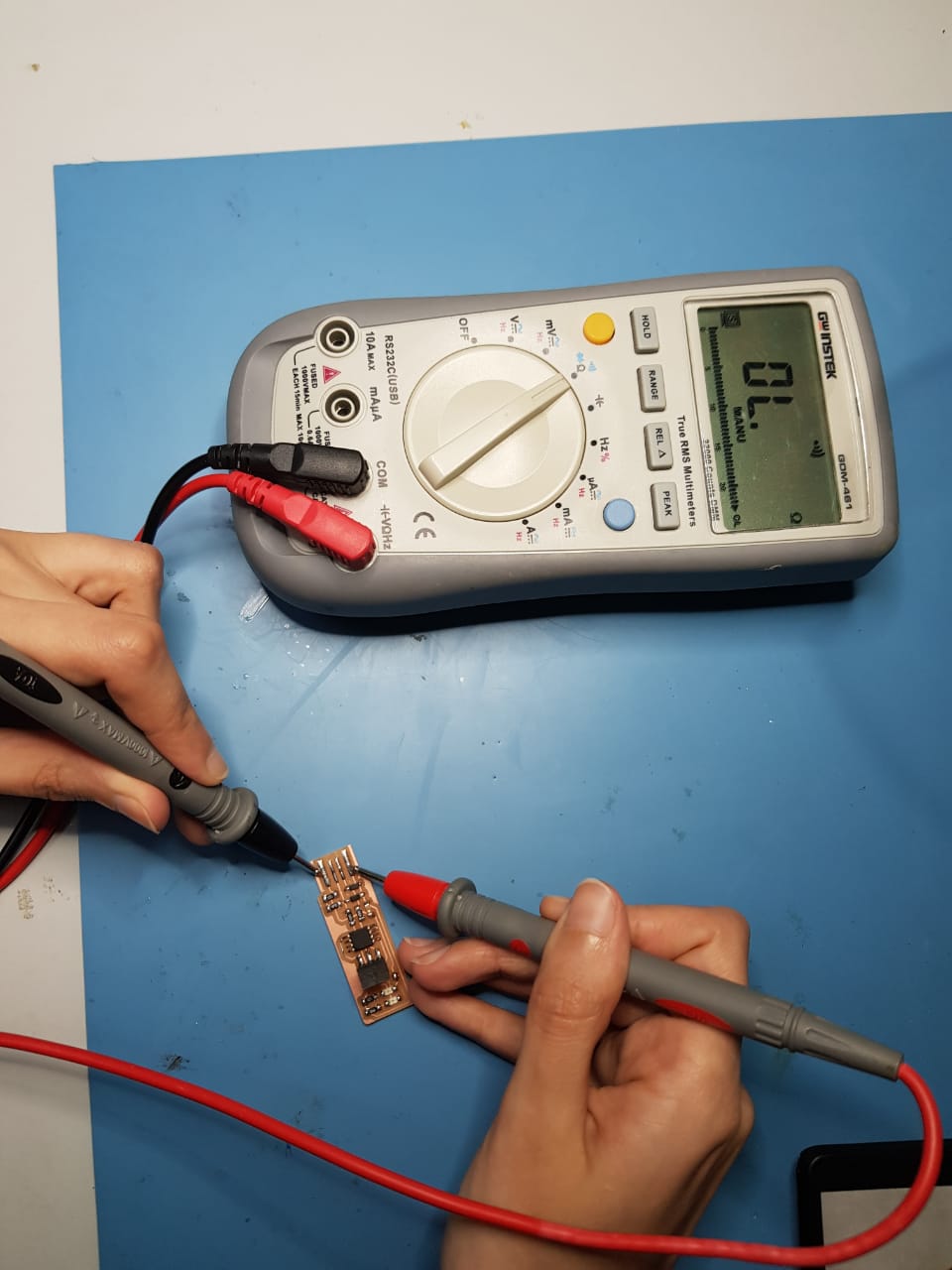
Finally I used the multimeter to check continuity between connected components and to ensure that there is no short circuit between VCC and GND.
2. Programming Fab TinyISP
First, I installed the following programs in my PC to setup the environment to be ready for programming the ISP:
- 1. WinAVR 20100110
- 2. FTS firmware
- 3. Zadig
- 4. GNU make
- 5. AVRdude
After installing WinAVR folder I needed to do the following steps:
(I reviwed Maha's website to do these steps)
1. Open WinAVR folder >> find bin folder and move the files avrdude.conf and avrdude elsewhere.
2. Replace the removed folders with the new version avrdude-6.3-mingw32.zip. All the versions are in this website.
3. Go to Control Panel > Systems > Advance System Settings > Environment Variables > Path > Edit > Delete the old AVR path and add the new path.
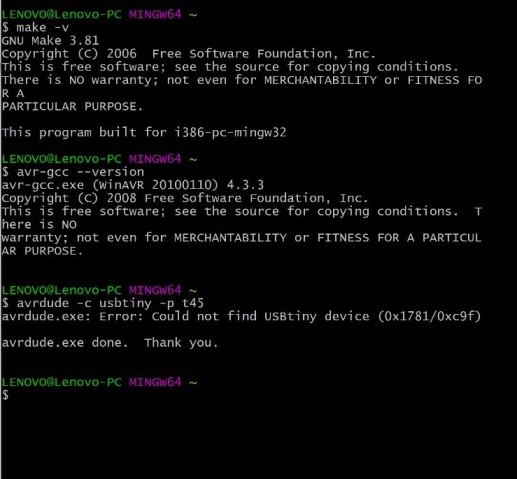
Now it's time to check from the terminal that all the programs were installed correctly.
To do so, I wrote these commands in Git bash.
make -v
avr-gcc --version
avrdude -c usbtiny -p t45
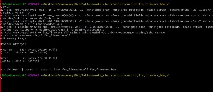
After installing the fts-firmware:
- I extracted the zip file then I typed make in Git bash to create a hex file.
- Here I connected my ISP with my instructor's ISP then plug instructor's ISP in the laptope as shown in the below image
Red LED is ON in both ISPs
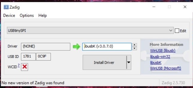
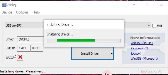
- Then I opened Zadig and I installed the driver in my ISP.
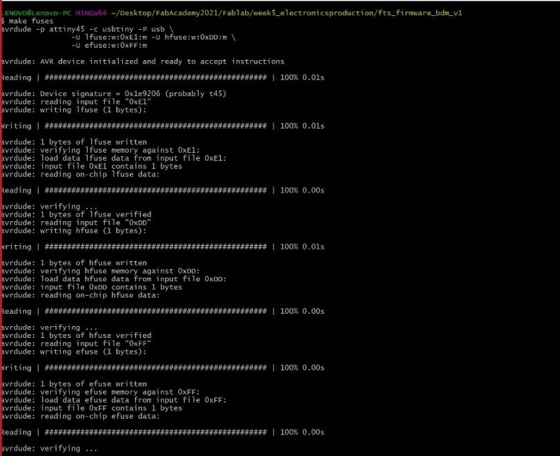
- Then I typed the commands make flash and make fuses
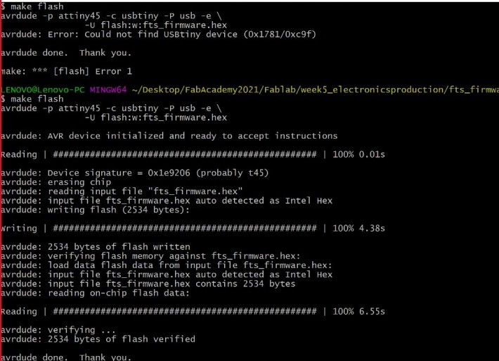
- After that, I pluged my ISP in the laptop directly.
In this step I realized that something went wrong because there was no sound while inserting my ISP in the laptop.
I noticed later that I soldered the zener diodes reversly.I removed them and re solder them.
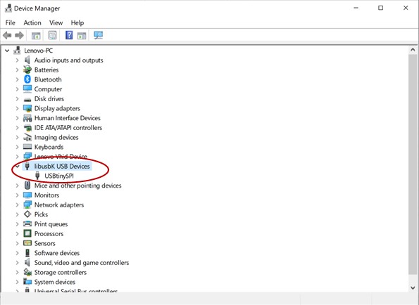
Then I went to Device Manager to check that my ISP appears there.
- Finaly I reconnected the instructor's ISP with mine and plug instructor's ISP again in my laptop.
I opened Git bash again and wrote this command rstdisbl
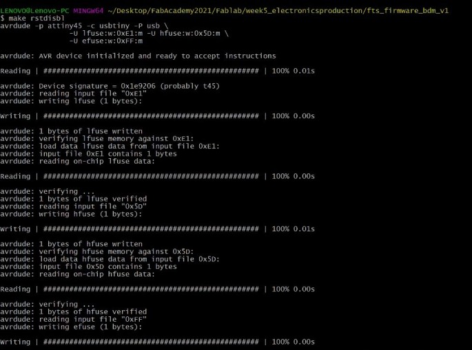
Now my ISP ready to program any board
I used my programmer to upload a blink code as shown in the following video.
Group Assignment
Group Page Link
For the group assignment we tried milling in two ways (Conventional & Climb)
by using two different milling bits (0.01 & 1/64)
I used fab modules to calculate PCB traces and use it for milling
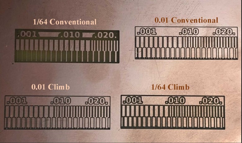
As shown, increasing the size of the milling bit will disappear some of the details.
The result of 0.01 milling bit in both climb and conventional is more clear and we can see the very small details.
Problems I faced:
- 1. I soldered the zener diodes in my ISP reversly. I noticed that I did something wrong when I inserted it directly to my laptope, there was no sound and my ISP doesn't appear in the Device Manager list.
Close Project