Electronices Design
Week Seven.

Week objectives:
1. Redraw Eco Hello world board by adding one input and output using " Autodesk Eagle" software.
2. Redraw Arduino (ATmega328p)
3. Using another software to do the Schematic and Layout.
Group assignment:
Use the test equipment in our lab to observe the operation of a microcontroller circuit board, for the group assignment visit our group page.
Used software’s:
Autodesk Eagle.
FlatCAM.
PCB Desgin steps:
Schematic.
Layout.
Milling.
Soldering.
Eco Hello world board - ATtiny44:
To design the PCB I used Autodesk Eagle, which is electronic design automation (EDA) application, schematic capture, printed circuit board (PCB) layout, auto-router and computer-aided manufacturing (CAM) features. Also, EAGLE is also an acronym for Easily Applicable Graphical Layout Editor.
Schematic Diagram:
A schematic diagram is a picture that represents the components of a process, device, or other object using abstract, often standardized symbols and lines.
It is easier to begin the PCB design with the schematic rather than the layout; having a clean schematic will make board routing easier.
The PCB design with schematic is made up of components and wires that are joined in a certain way to create an electrical circuit. In layman's terms, a schematic diagram depicts how the various components of a circuit are connected to one another. The illustrations explain how lines indicate connecting wires; otherwise, fundamental components such as resistors, bulbs, and switches are represented by symbols that are consistent.
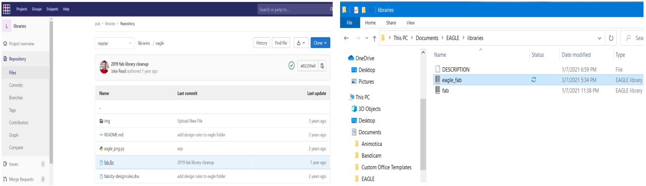
First, I will added the components I will need from Fab library they must be available in the Lab.
The steps of adding library in Eagle the following:
1. Open Eagle folder.
2. Download the fab file with .lbr extension.
3. Add it to Eagle libraries and save it.
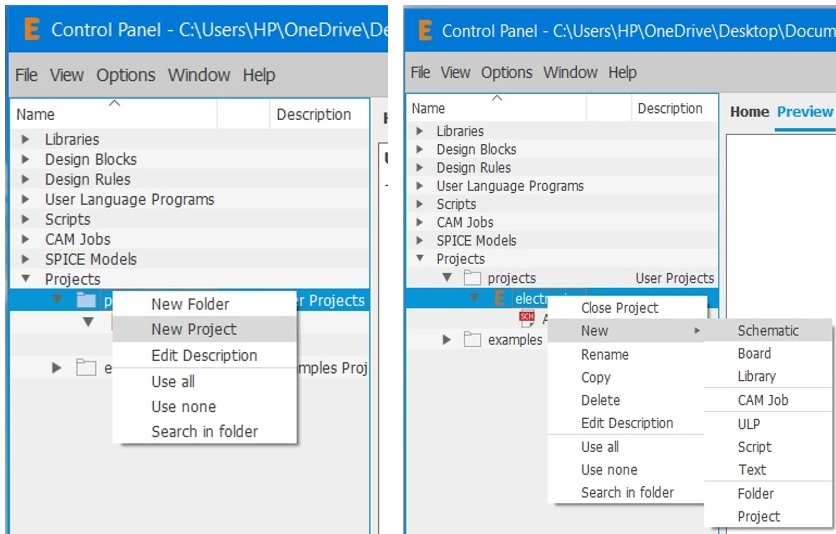
I created a new project
Select New >> Schematic as shown below:
Used Components:
1. ATtiny44.
2. Resistor “R1=10K ohms”.
3. Capacetior “C1= 1 MicroF”.
4. XTAL Resonator 20 MHz.
5. FTDI connector (1x6 header).
6. ISP connector (2x3 header).
I did add:
1. button (input).
2. Red LED (output) with Resistor “R2= 499 ohms”
I utilized the LED as a limiting resistor because the smallest accessible resistor value in the lab is 499 ohms.
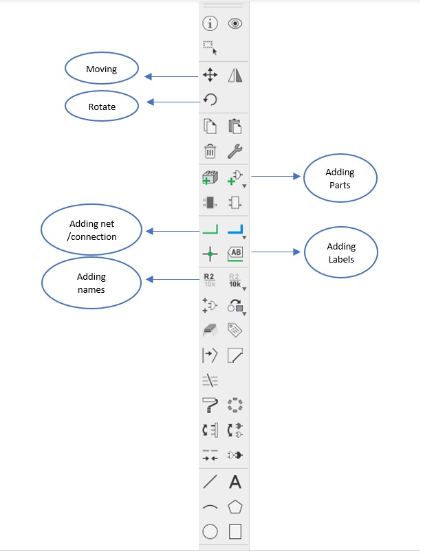
To control in Eagle using Command Toolbar, the image below shows the important symbols:
The image shows the final schematic, I redrew echo hello world provide in fab academy website. here is the ATtiny44 data-sheet:
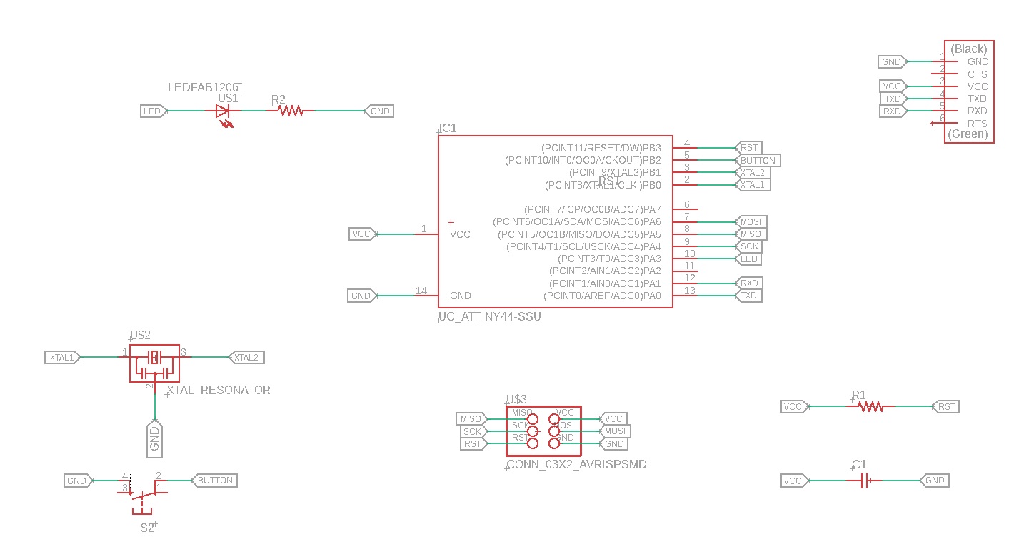
After checking that everything are connected in the right place
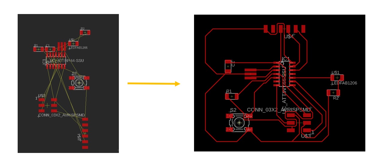
I converted the Schematic file to the Layout file as shown below:
Layout :
The created board with yellow color airwires required to be routed, as well as the components generated in random regions, so I had to choose where to position them in the board before routing them. The arrangement of components is critical; incorrect placement might make routing difficult or impossible.
Important Notes:
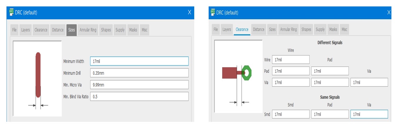
review the design rule check (DRC) before routing
I changed the clearance to 17mil to match CNC machine settings.
I reduced the width of traces to 12 mil instead of 16 mil to allow for more space for the tracks to pass through.
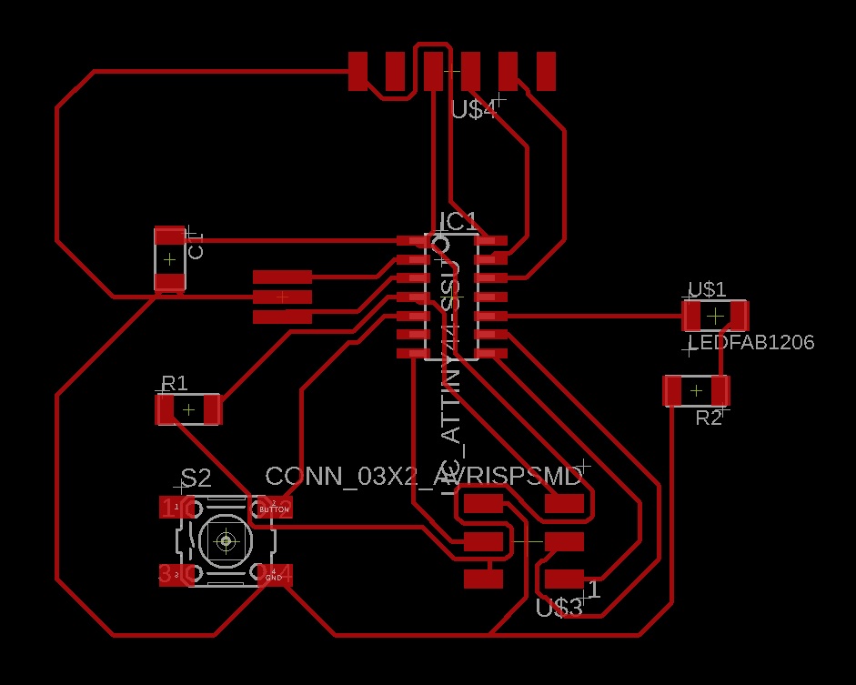
The picture below shows the final layout:
As shown below the steps of exporting the layout to images, to use them afterward in fabmodules:
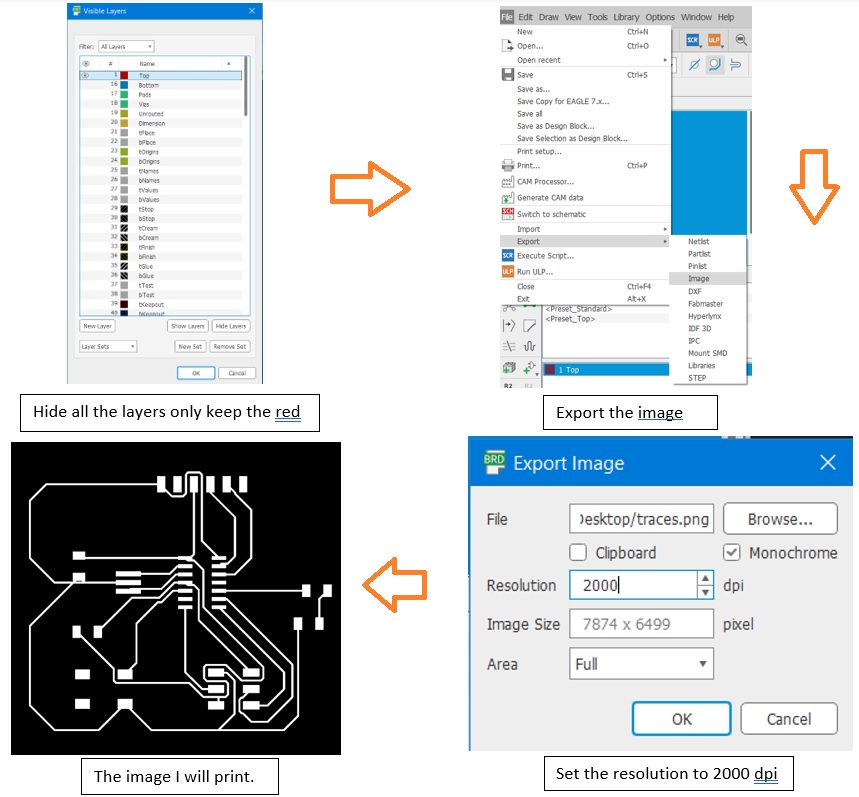
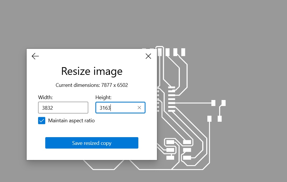
I needed to check the resolution of the PCB images
I reduce it down by 50% to get the original size by using resize as shown:
Redraw Eco Hello world board by using " Autodesk Eagle" software.
Add (at least) a button and LED (with current-limiting resistor).
Add at least one inputs and outputs
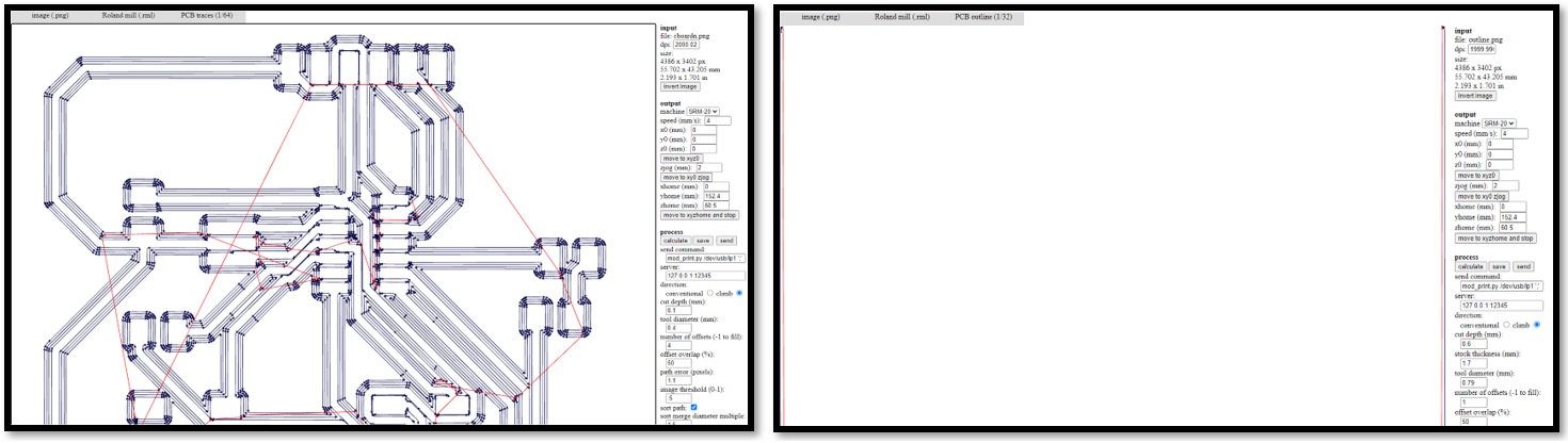
Fabmodules files:
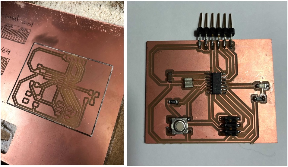
This is my final PCB board after soldering:
The board was placed on the fixed aluminium profile (back side).
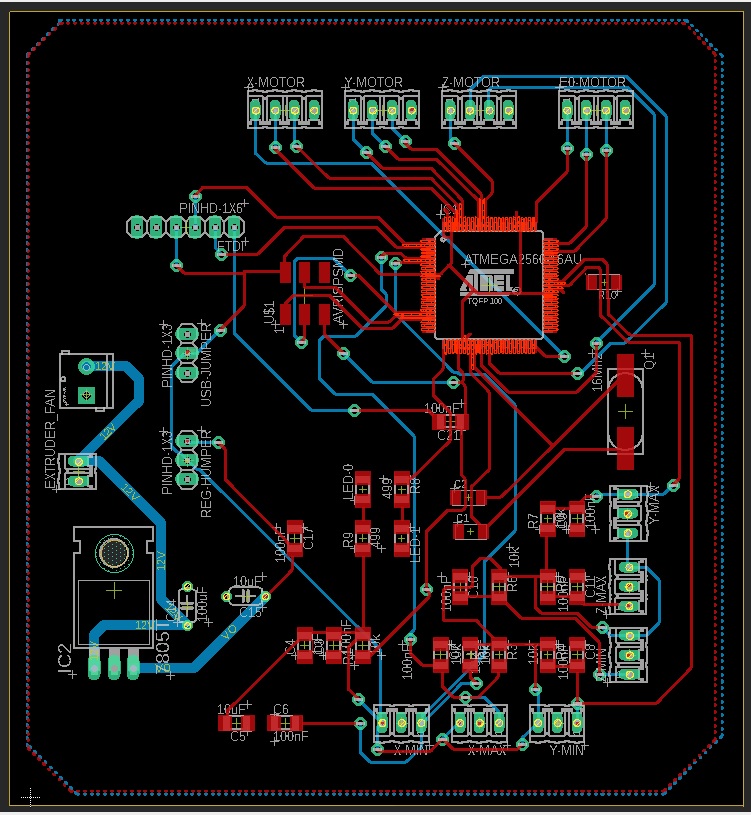
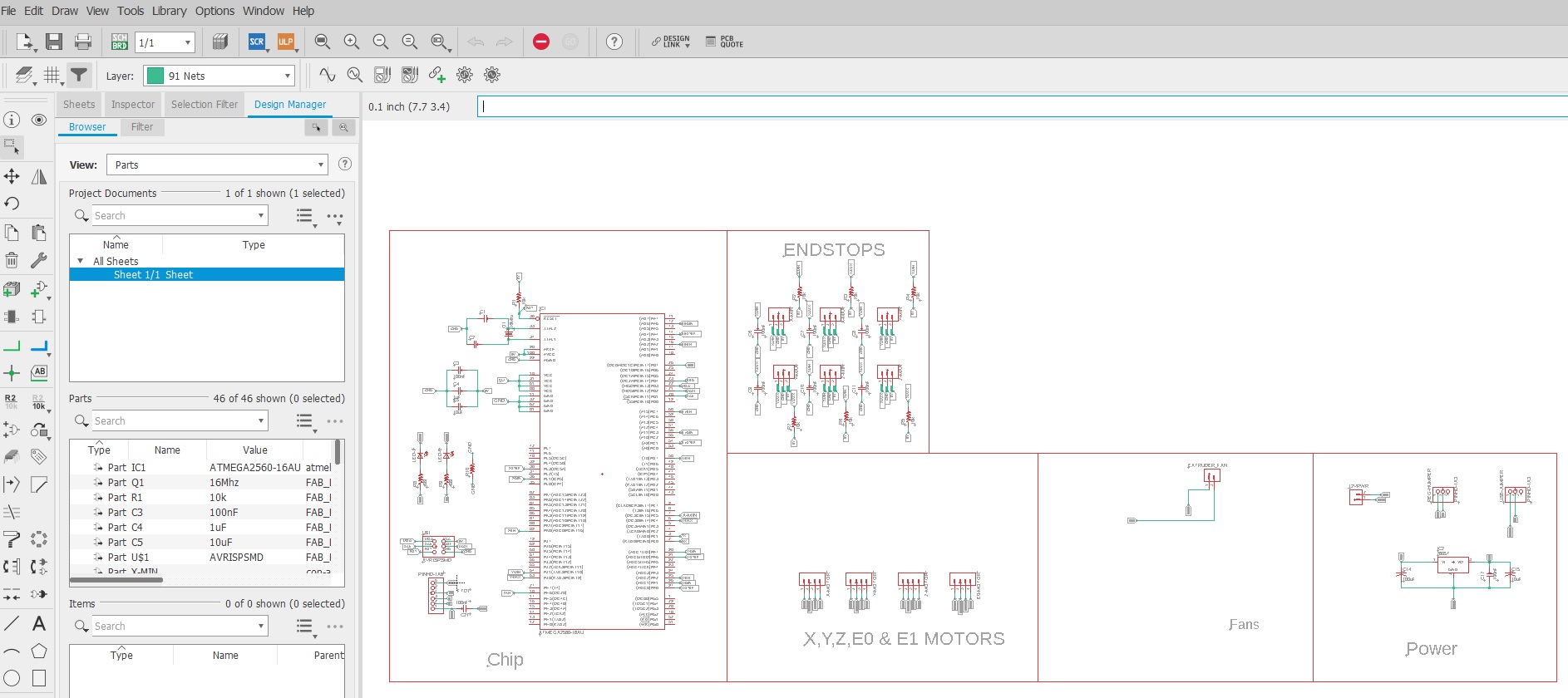
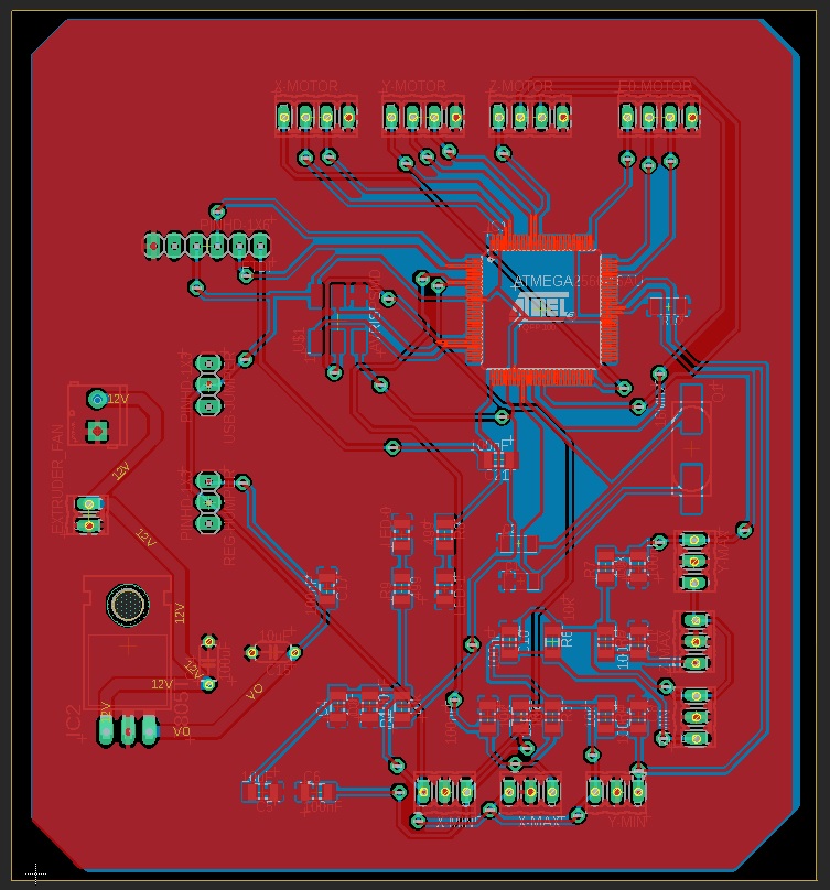
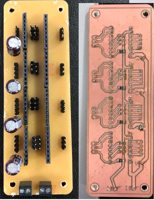
I start to design my first double-sided board for the project.
The FabRamp board is already an open-source board.
The board was designed by my instructor Hashim Al Skkaf in Fab Academy UAE.
RampBoard
Manufacturing
Usually for PCB milling I use CNC machine in fab lab.
I use the FlatCAM to generate the g-code.
FlatCAM is free software that converts Gerber to a single G-code file that integrates the paths and drill files, than we can use the Milling Machine Software.
For this kind of machine, we command & using the machine software.
Results:
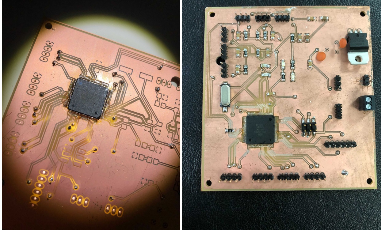
Assembling:
The processor was difficult because of the numbers of components to be solder.
The board was double-sided, so it was difficult to deal with it was first time experience.
It was difficult to take it out and it is almost damage.
The processor of soldering should be starting from the vias to the rest.
The Atmega 2560 clearance and distance is less than 0.4 or 1/64 inch so we need to use milling bit with 0,15mm and the rest of milling traces the normal 0.4mm milling bit.
The first step is to export the file to flatCAM file>>cam processer>> process job>>select place>>ok
Flat CAM
Setting
Open flatCAM>>edit>>unite>>mm
We will put the same speed that we are using in fab modules.
Geometry>>end move Z(80)>>Feed rate x-y ( 280)>>feed rate z(60)
Travel z (2)
To open the graber files >> open >>open graber
We will start with the copper_top>> select
we will set every part
Because it is double side PCB we will do the top as will For the bottom
The steps will be repeated for the similar parts
To open the graber files >> open >>open graber
Then the copper_bottom>> select
The cut Z (-0.1) >> Generate CNCJOB object
For the second board I will be used for stepper motor
I will start with the top copper
Project >>copper_top
Selected >> tool dia (0.4)
Passes (4)
Pass overlap (50%)
Chose climb >> combine >> All >> full
Then Generate isolation Geometry
For the geometry object
Cut Z (-0.1)
Travel Z (2)
Generate CNC job object
Then save CNC code
File >> open >> open Excellon
To do the hols in the board I need to do the steps below
Go to project >> right click >> Edite >> close edit
Because there is too many size of drills and I will use one size in the machine it is hard to use that much of sizes
The size I chose is 0.8 (1/32)
Excellon object
Drill >> cut Z (-1.7) >> travel Z (2)>> end move Z (0.5)>> feed rate Z (300) >> drill tool (0.8)
Create drills Gcode
To do the hols we will use the same steps before
I will repeat the same steps for the stepper motor PCB.
Results:
_______________________________________________________________________
Please find the attached files: