Week 4
In this week I was introduced to the world of electronics and I was kinda scared because I never dealt with these things before however I was excited to try and test the milling machine and manufacture some PCB's , this weeks assignments :
- Group assignment: Characterize the design rules for your PCB production process: document feeds, speeds, plunge rate, depth of cut (traces and outline) and tooling, document your work (in a group or individually).
- Individual assignment: Make an in-circuit programmer by milling and stuffing the PCB, test it, then optionally try other PCB fabrication process.
Learning outcomes
a. Described the process of milling, stuffing, de-bugging and programming
b. Demonstrate correct workflows and identify areas for improvement if required
Line test:
we have the roland SRM-20 in our lab and we will be using it for milling pcbs and molds:
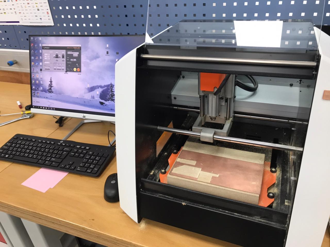
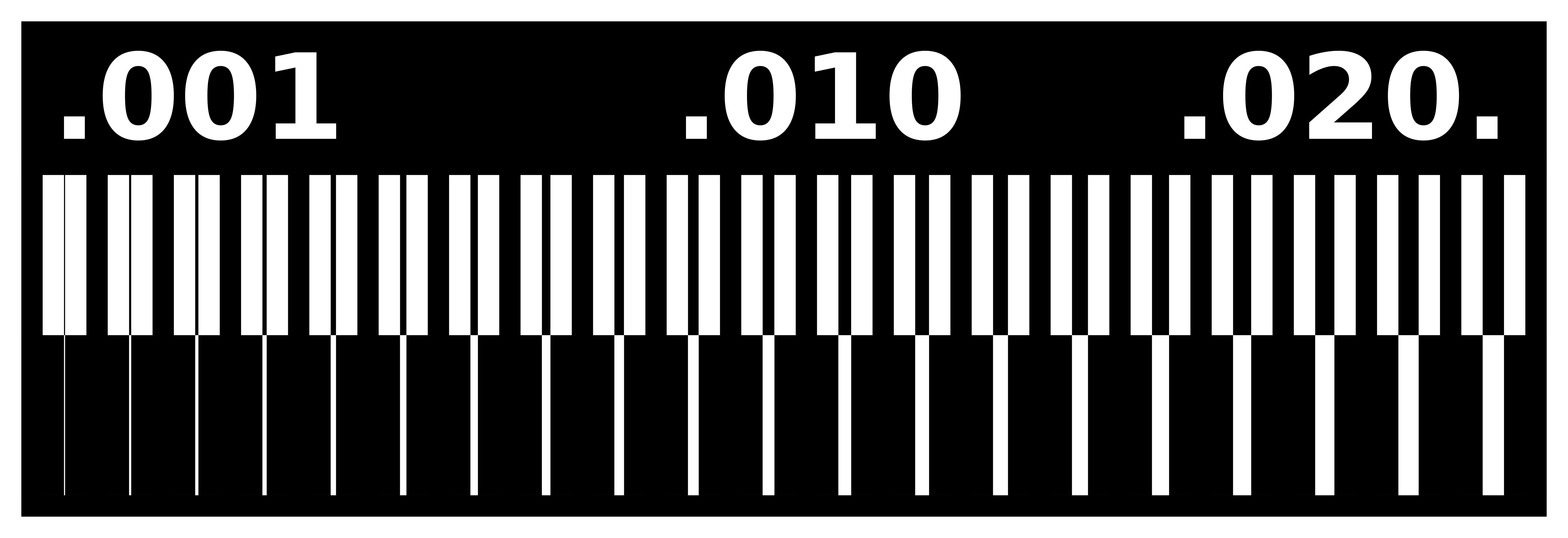

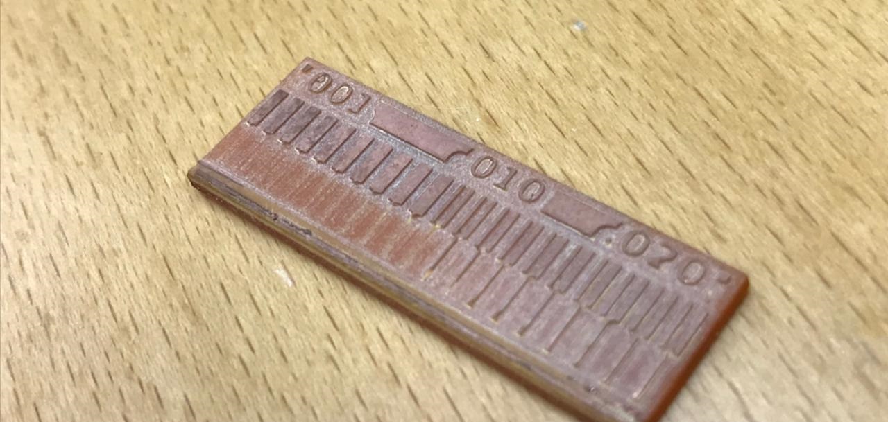
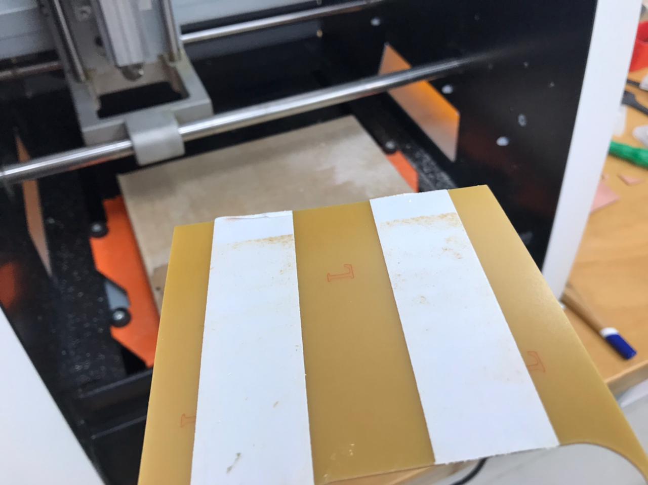
The two main factors that we were testing are :what is the maximum space between two traces and how thin can our traces be so as you can see in the picture our tool can fit up to 0.001 but the traces cant be as thin as 0.001 otherwise they will come off of the board.
Milling workflow:
Since all we have is ATiny45 so I went for brian's ISP because it seems to be working for most people and it is very well documented, I began
- start by downloading the PNG files for both the traces and the outline from brian's page :
- set the cupper sheet for the machine by adding double side tape on the back then stick it to surface.
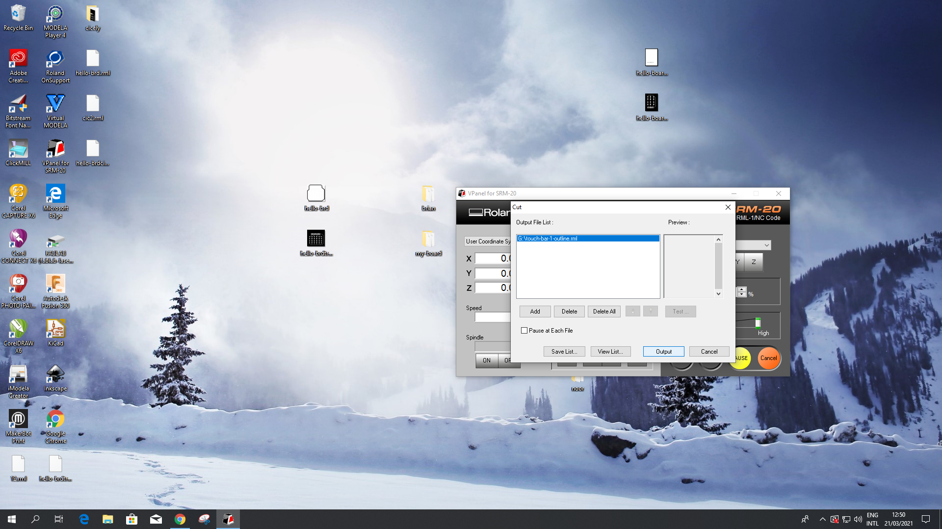
- connect your machine to the computer and open V-panel
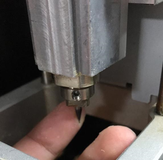
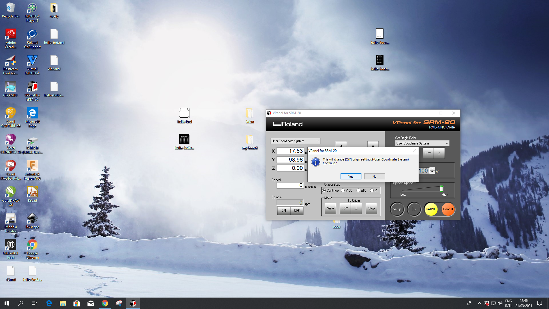
- First zero the z-axis and zeroing the z-axis is very important and It must be re-adjusted everytime the tool is changed , to zero the z-axis :
- change the tool and push it all the way inside in a way only the flute is visible
- carefully move it down using V-panel but do NOT let touch the cupper plate because some tools are very fragile , now adjust it manually so it is touching the plate
- finally set the zero origin for the z-axis in v-panel
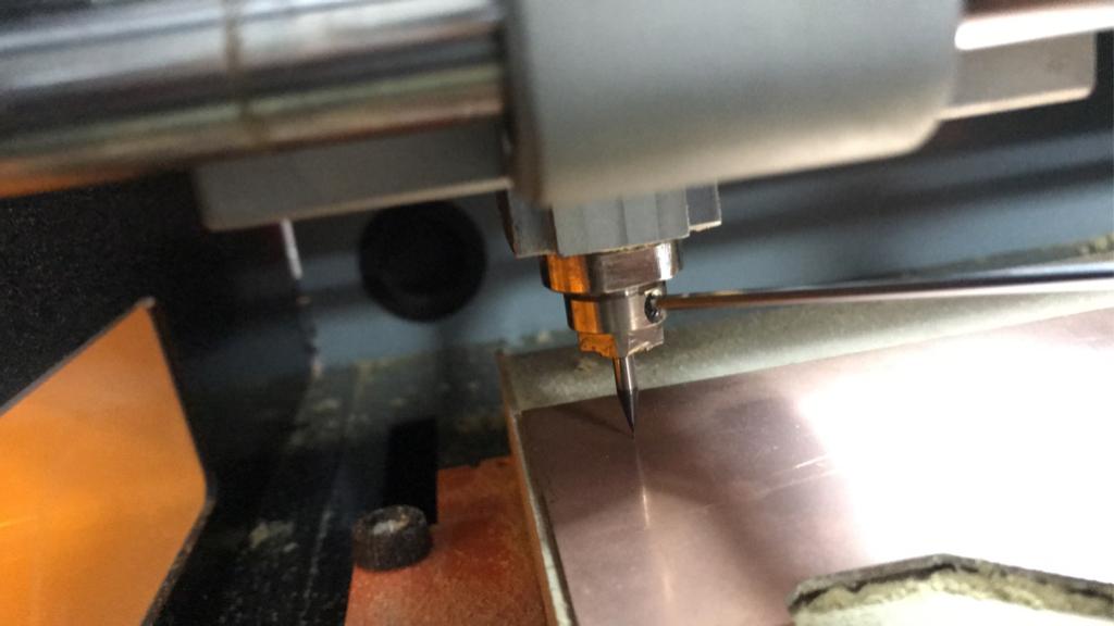
- Zero the x and y axis by moving with vpanel but make sure that the tool is not touching the plate otherwise it will break.
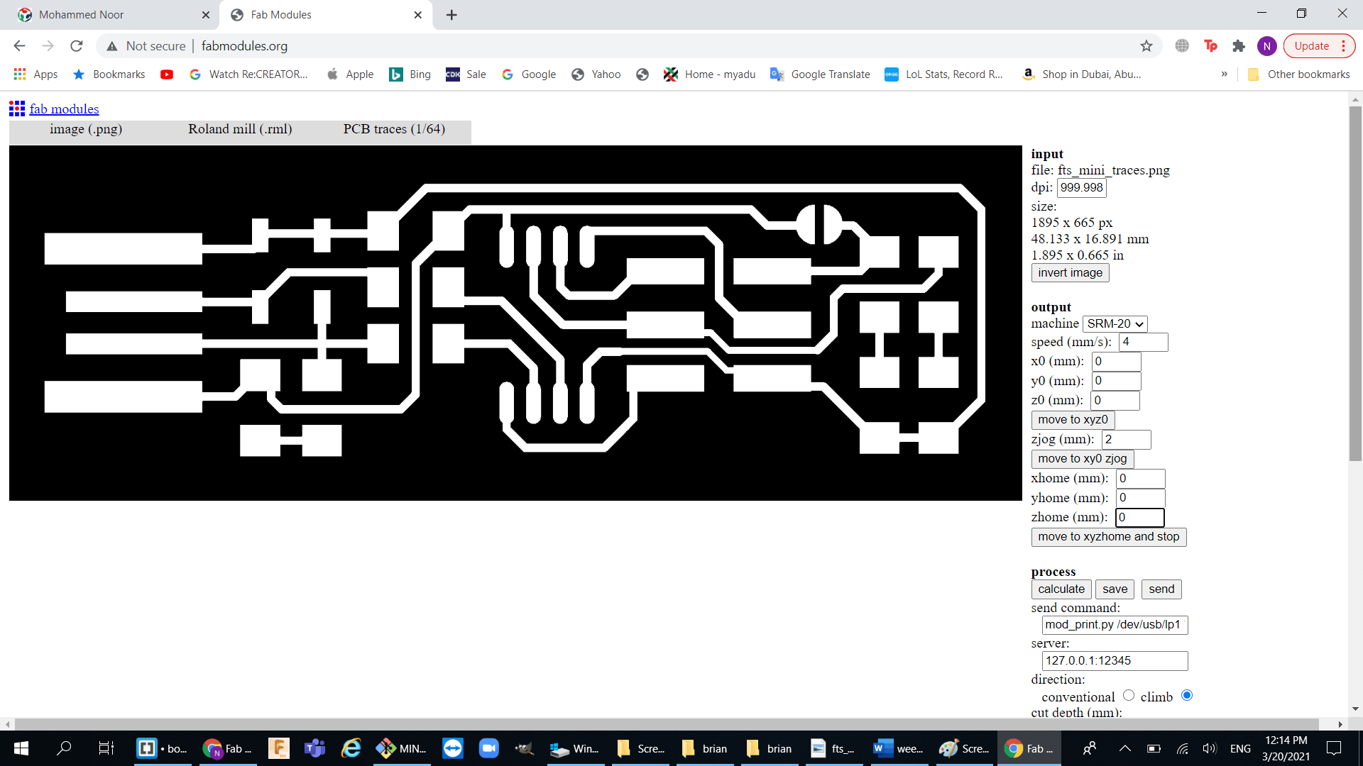
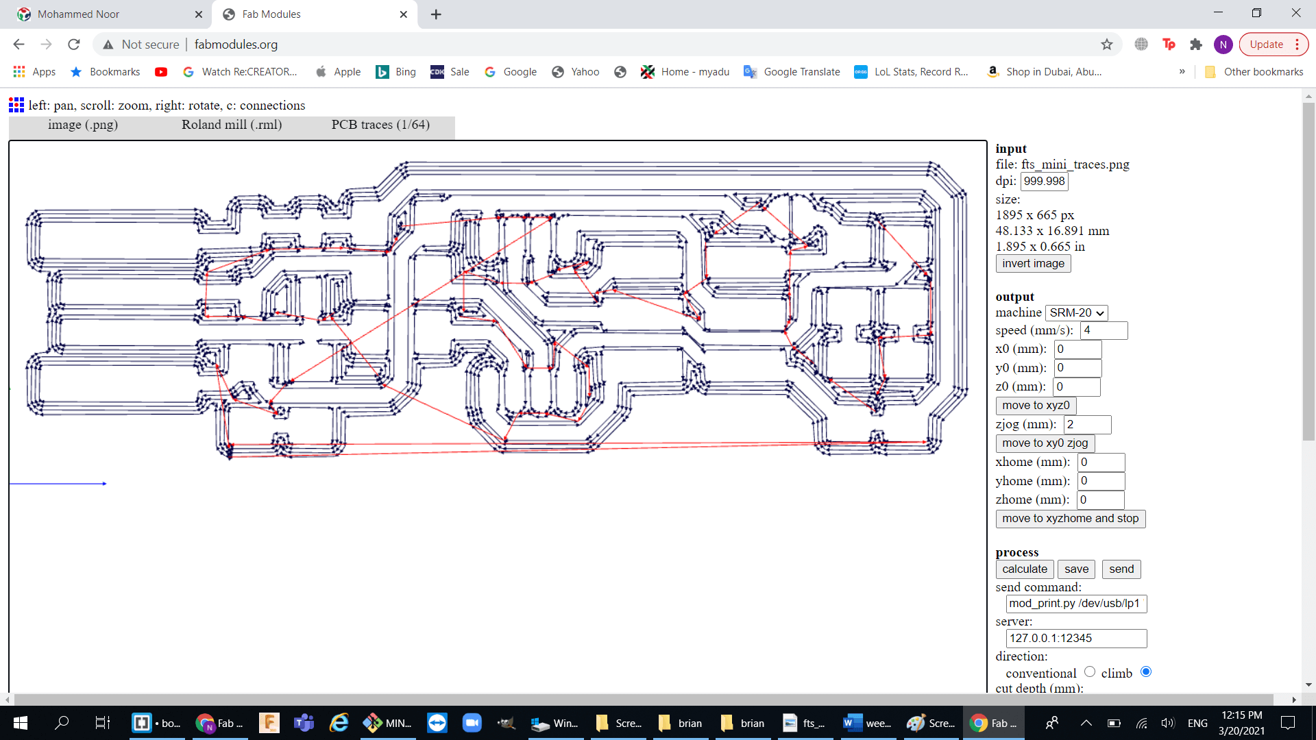
- Now go to fabmodules.org. this website calculate the tool path and gives you the file that is Compatible with your machine.
- Export your files and choose your machine and v-bit you are going to use
- Set the cut depth to what you want
- Now calculate then save
- I kept the speed as default 4 mm/s
- I changed the offests values to 0 in the x ,y , and z direction
- in this picture I set the xyzhome to 0 but actually I kept them default as this will bring the bed upfront and lift up the tool which very practical
- I used the climb milling method because it reduces the load from the cutting edge which leaves a better surface finish.
- Start cutting
- Milling The FabISP:
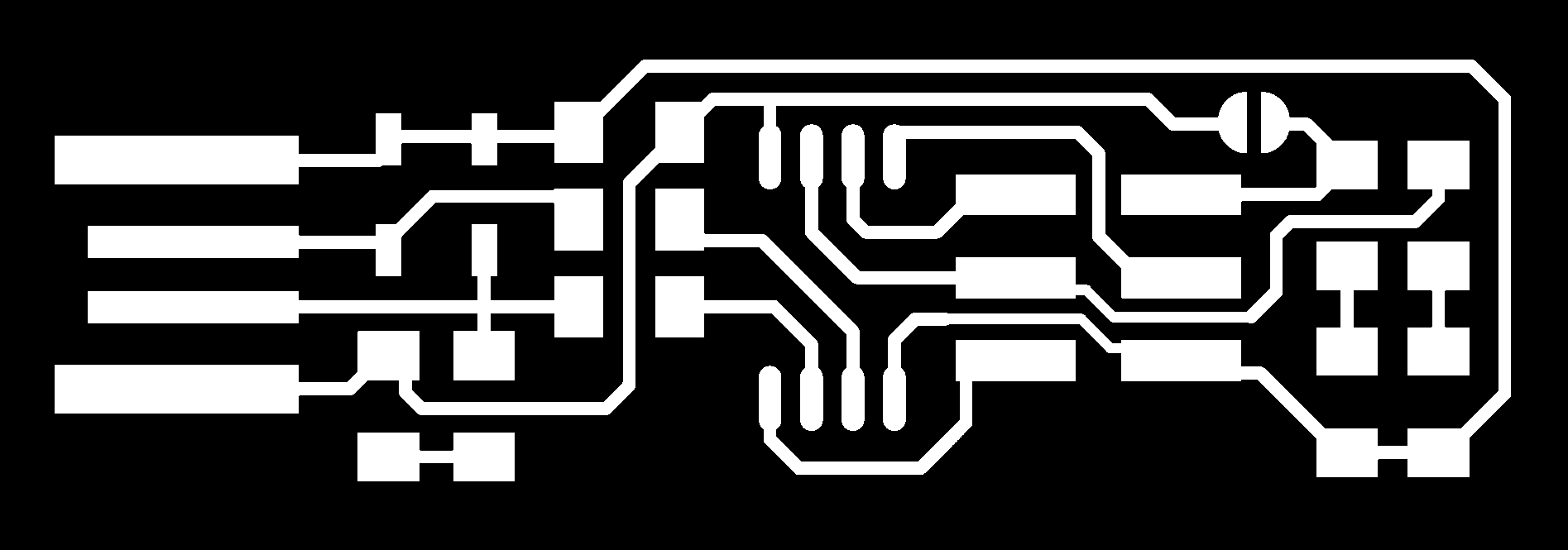


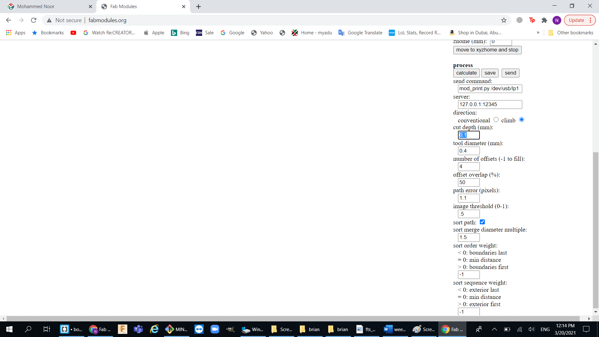
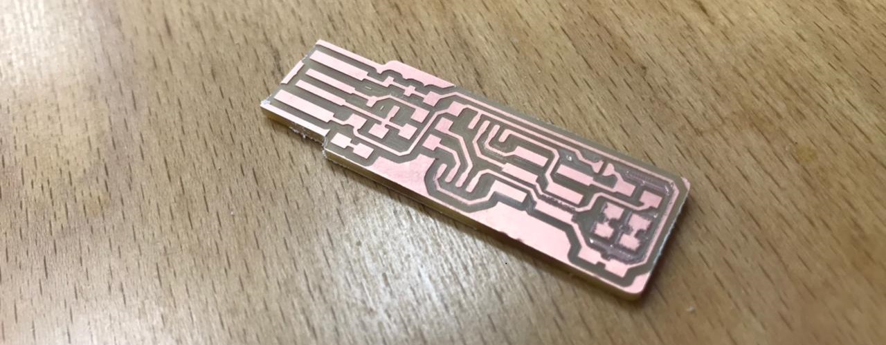
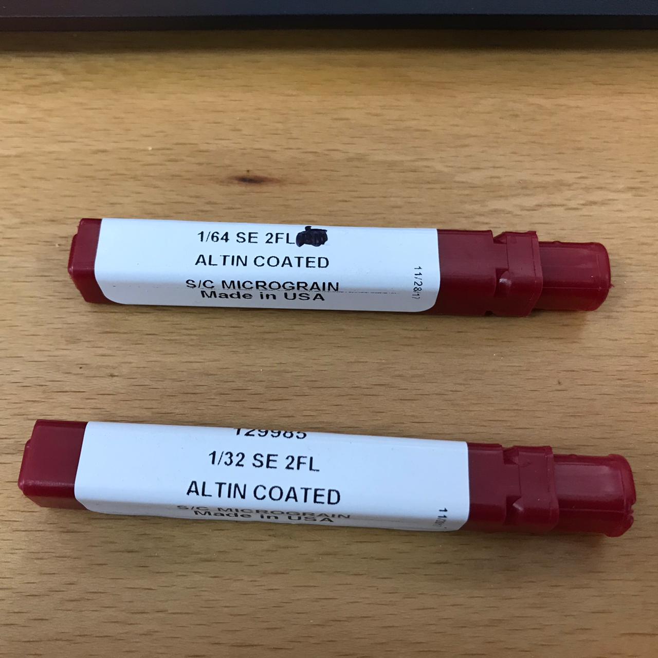
we used two kind of v-bits:
a. 1/64 for traces with 4 offsets and cut depth of 0.15 mm
b. 1/32 cutting with 3 passes and and total cut depth of 1.7 mm
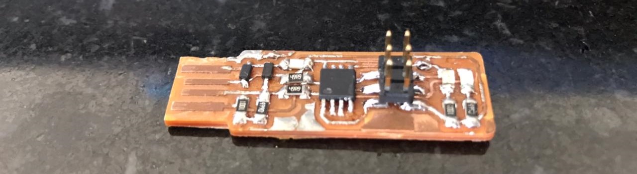
Soldering and stuffing the pcb :
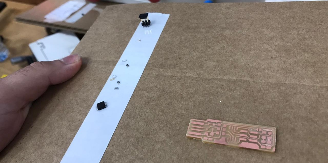
It was not an easy task for me to do because as I said I'm an absolute beginner when it comes to electronics,The components needed to brian's programmer:
- 1x ATtiny45 or ATtiny85
- 2x 1kohm resistors
- 2x 499ohm resistors
- 2x 49ohm resistors
- 2x 3.3v zener diodes
- 1x red LED
- 1x green LED
- 1x 100nF capacitor
- 1x 2x3 pin header
Soldering workflow:
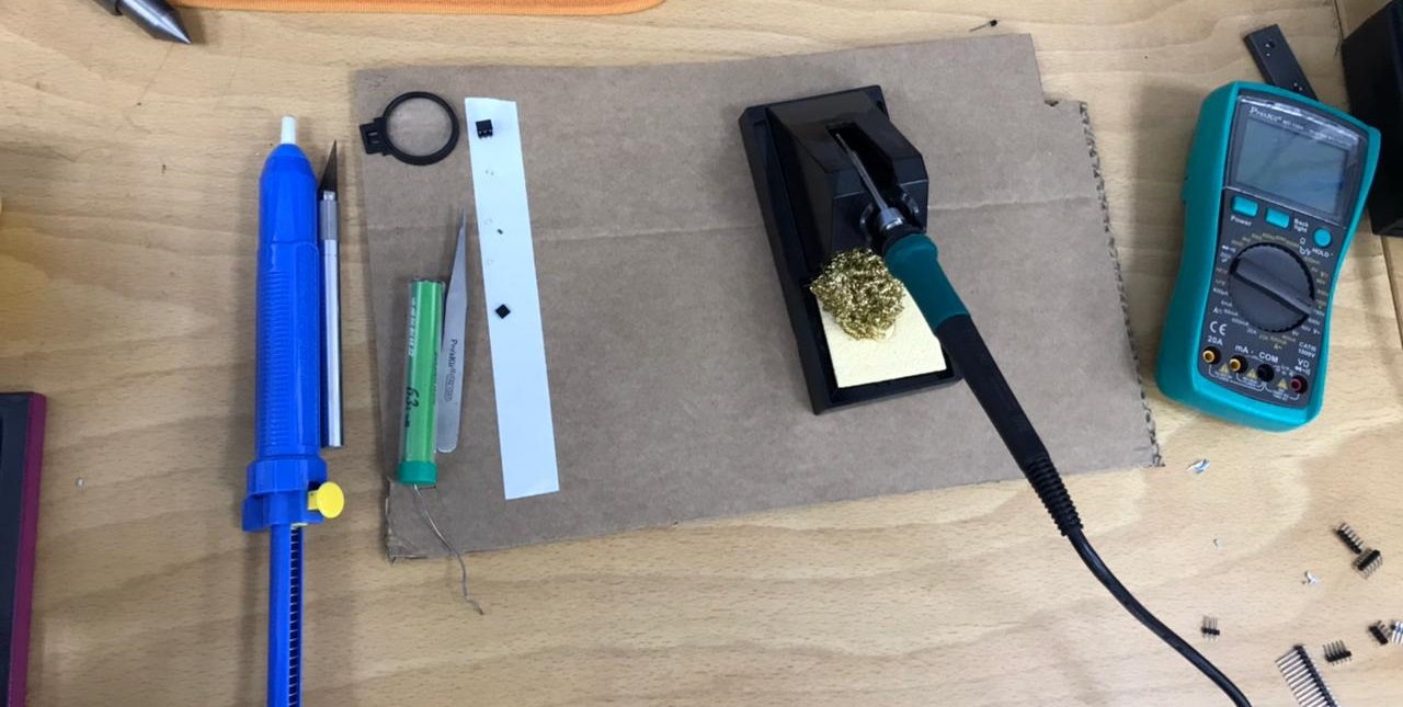
- Prepare the soldering equipments : the soldering iron , tweezers , solder , the sucker , magnifying lens , light , and some tape .
- Prepare the pcb and the components by taping both the board and the components to a double-sided tape
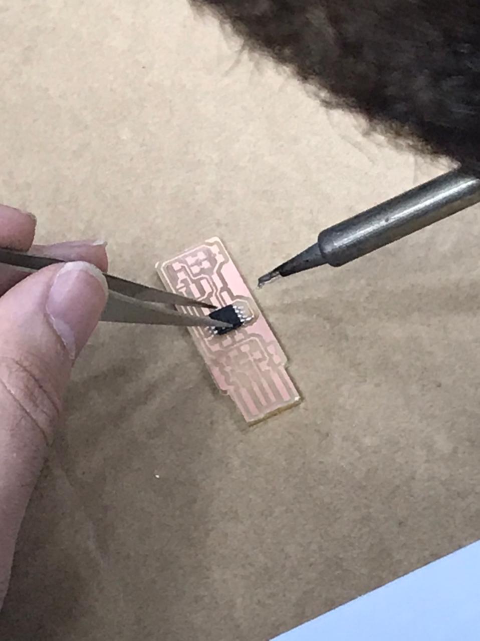
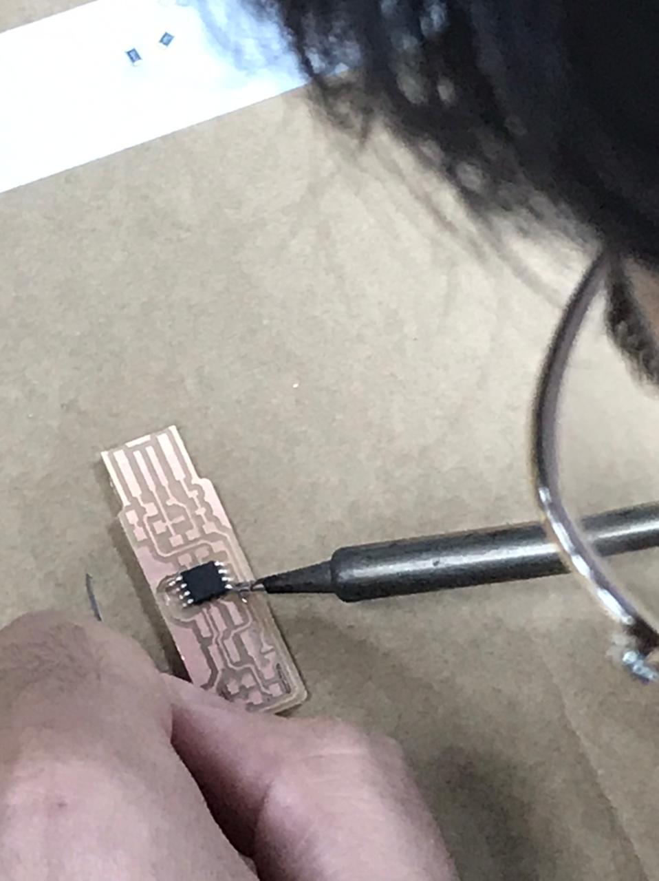
- Start soldering the components from inside out by doing the MC first then the ISP header then the diodes and resistors and keep the pins till the end
- when soldering a component adding solder to one pad then use the tweezers to place the component on the same pad then solder the second or third pad and finally go back and re-solder the first pad( this process called Tacking).
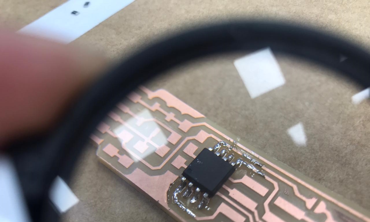
- finish up by checking each component with the magnifying lens
problems I faced while soldering this programmer:
- I did not know the direction of the diode as it was not so clear to see
- Soldering the micro-controller was a bit difficult because the pads were kind of small and close to each other's
Programming it:
To be frank with you, this was the hardest part of this assignment because it was quite difficult to make the programmer work using widows however brian posted a guide on how to do it but it wasn't enough and I did some digging and here's the steps :
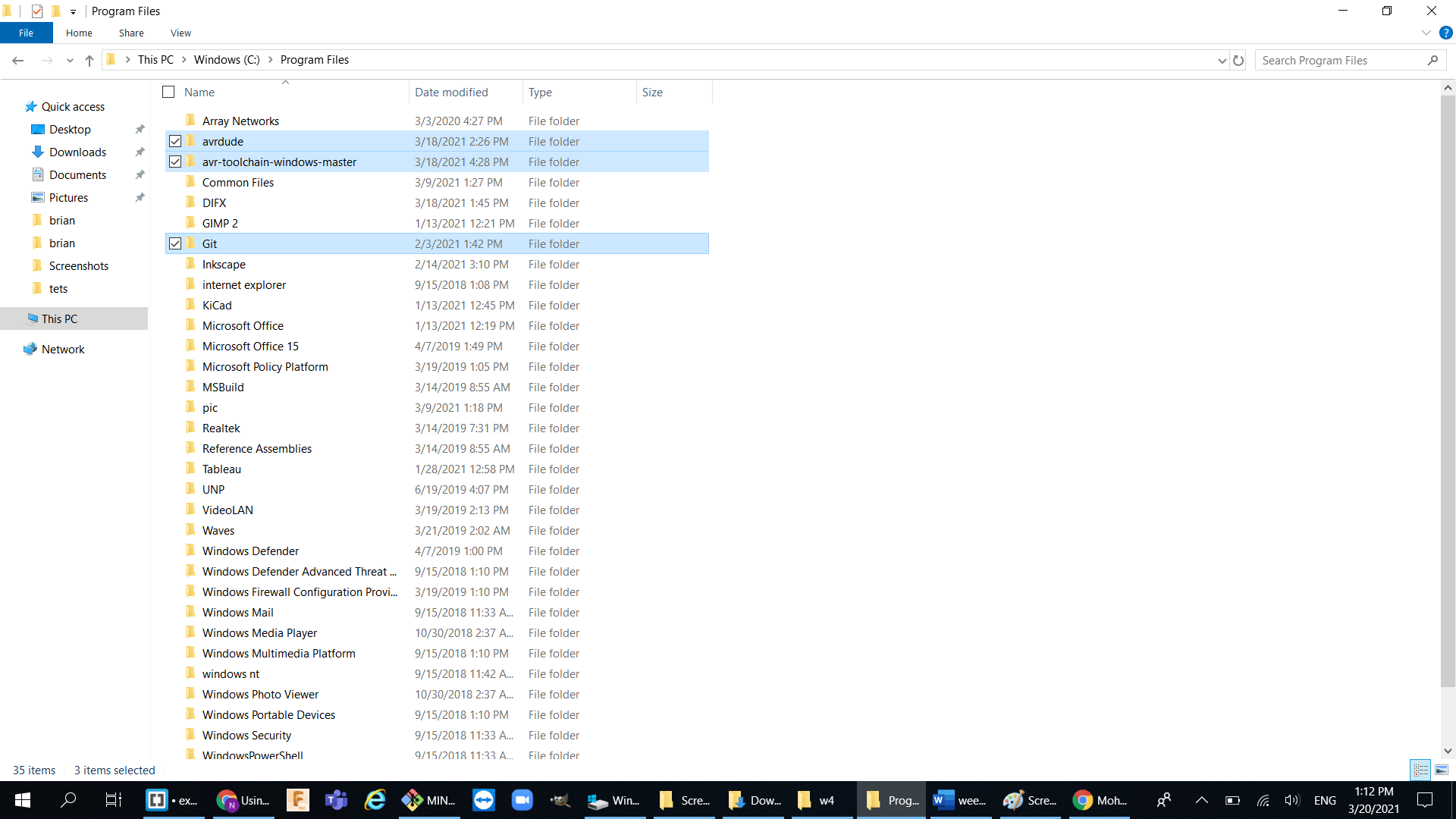
- Start by downloading these git atmel GNU toolchain GNU make avrdude and extract all of them to C:\Program Files (it was really hard to find the right toolchain but thanks to this guy ,he had linked it in his page)
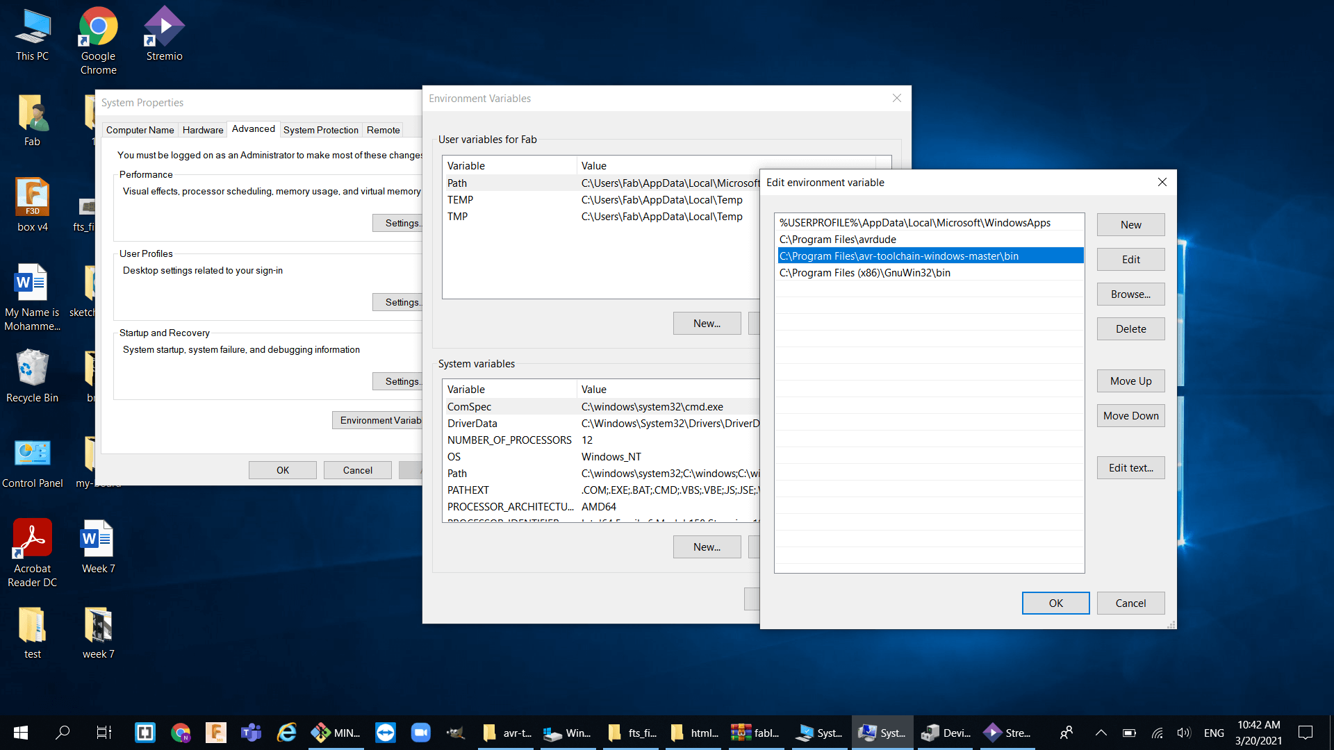
- Update your path , make sure you have these 3 values :
C:\Program Files\avr8-gnu-toolchain\bin
C:\Program Files (x86)\GnuWin32\bin
C:\Program Files\avrdude
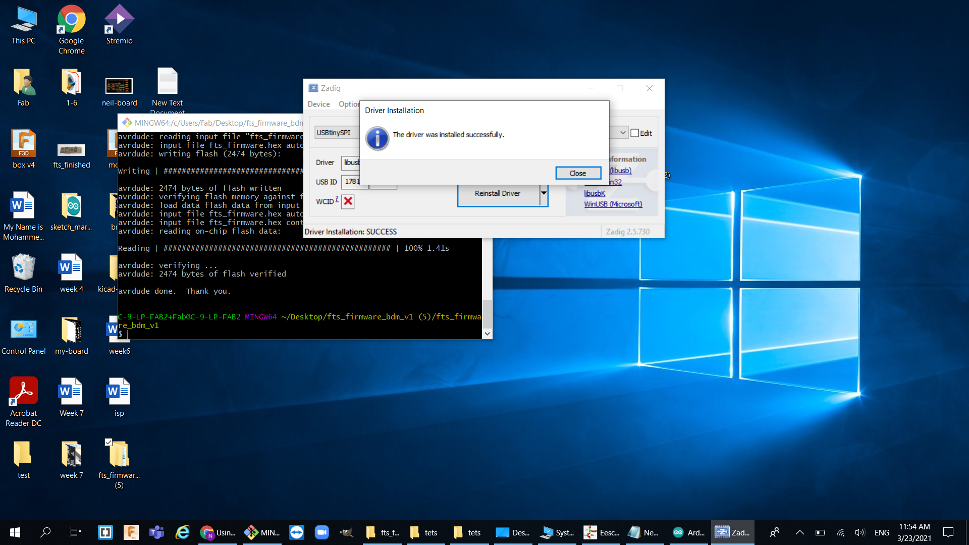
- Install zadic
- Download the firmware
- Open git bash and direct to the downloaded firmware then run
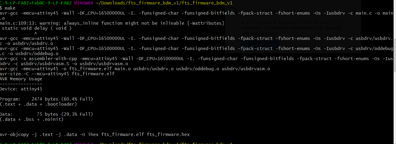
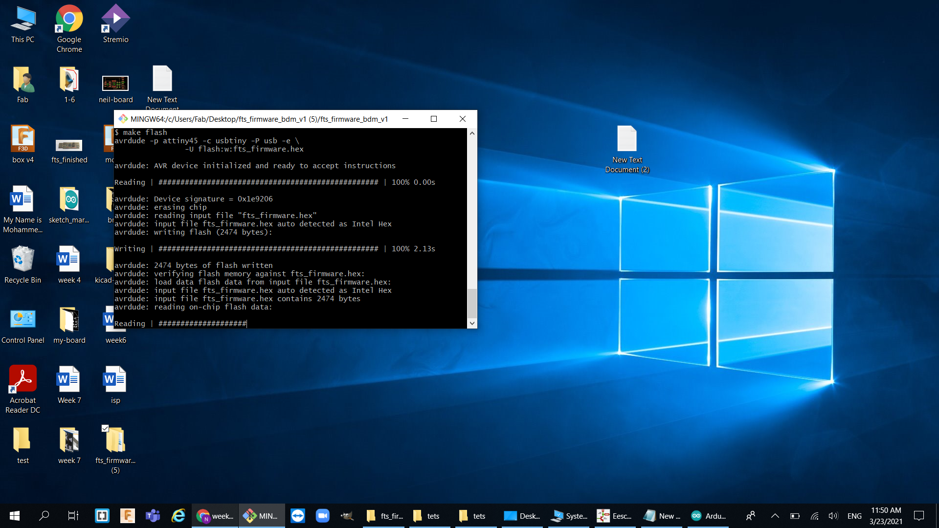
maketo create the main.o file - I used my instructor USPTiny programmer to programm my FabIsp after failing many times to programm it using the ArduinoISP :
- Now go back to and run
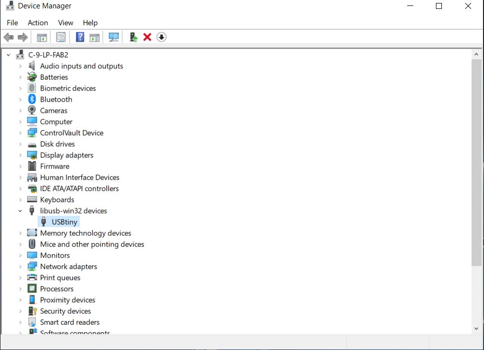
make flashandMake fuses: - Lastly connect your programmer to your computer and open zadig and install the Libusb-win32:
 />
/>
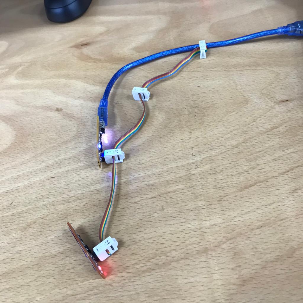
Final result:
Things I have learned while soldering:
- Always prepare everything before you turn the iron on, once all the equipments are ready turn it on
- Double sided tape is very useful when soldering because you can just stick all the components to it as well as the pcb
- The temperature of the soldering iron shouldn't be too high, so it doesn't burn the pads. for me a temperature of 300-340 C was enough to melt down the solder
- Adding more solder will fix most of the problems when soldering like having a blob of solder because when more solder is added it will make it flow a lot easier.
- Cleaning the tip of the solder iron is very important because when it is dry it will affect the fluidity of the solder.
- the most useful tool when soldering is the sucker as it will magically remove the unwanted solder off the board.
- Finally, after finishing soldering the pcb adding some solder to the tip will save the tip from getting dry over the night.