6. Electronics design
Assignments:
Individual assignments:
- Redraw an echo hello-world board.
- Add (at least) a button and LED (with current-limiting resistor).
- Check the design rules, make it, and test it.
- Extra credit: simulate its operation.
Group assignment:
- Use the test equipment in your lab to observe the operation of a microcontroller circuit board.
Hello world board
The hello world board is a simple electronic circuit that allows serial communication with any device that supports this type of communication, such as laptop or another microcontroller.
The main goal of this week was to design a “hello world” board while adding some basic functionalities to it. I dediced to add a lock mechanism controlled via a push button as it will be useful for my final project.
I did not start from scratch as a whole bunch of hello world designs were provided in this Fabacademy page, for several common microcontrollers. As this program is fairly simple and does not require a lot of memory, nor many inputs/outpus I have decided to use an ATtiny45 microcontroller. Moreover, there were 2 unsuded pins in this microcontroller for the hello world application so it was just what I needed for adding my lock mechanism. I also made this choice because during the electronic production week, I produced a FabTinyISP based on the same microcontroller.
Here below is what I used as reference :
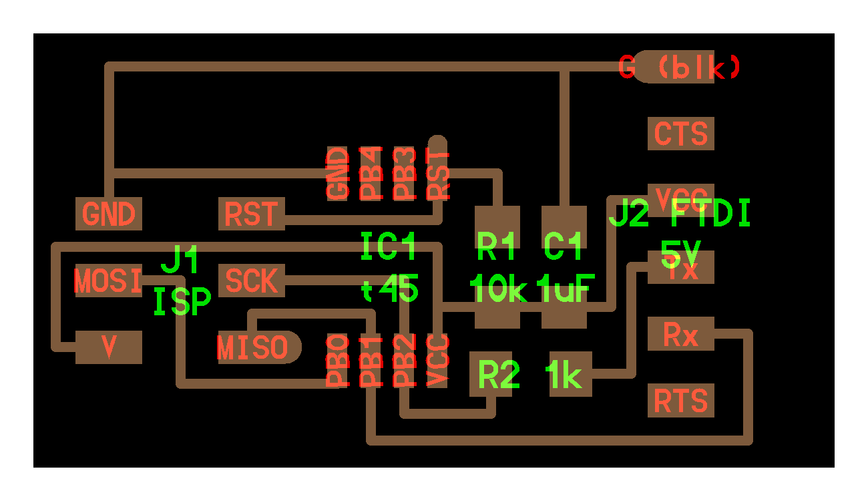 |
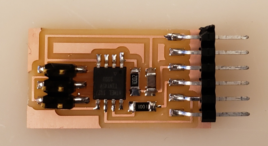 |
| Hello world example - schematic | Hello world example - final PCB |
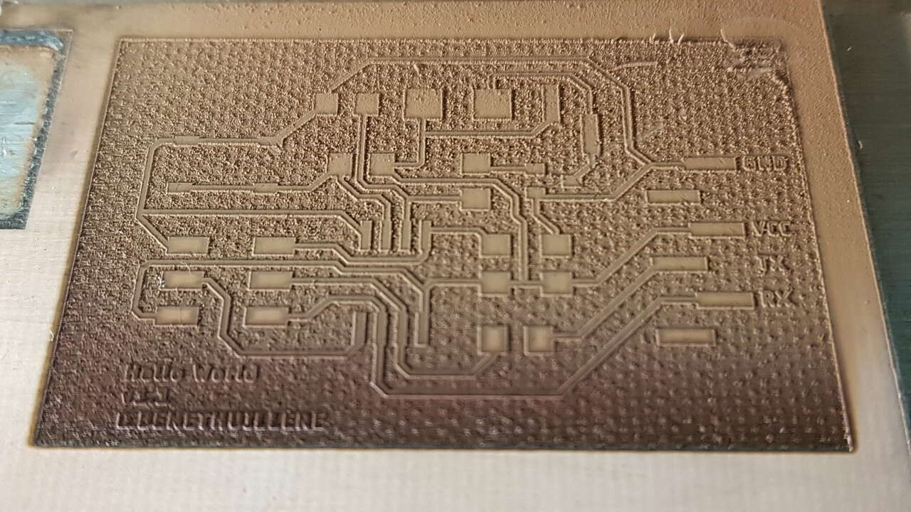
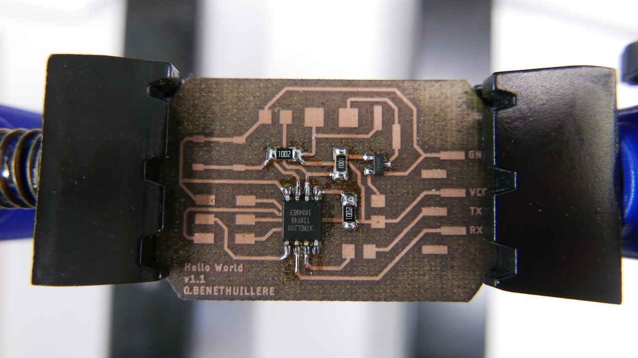
And here is what I achieved in the end :
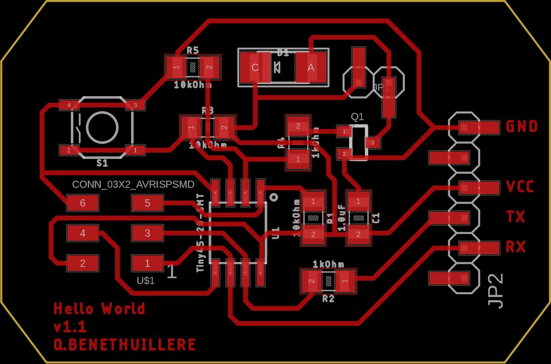 |
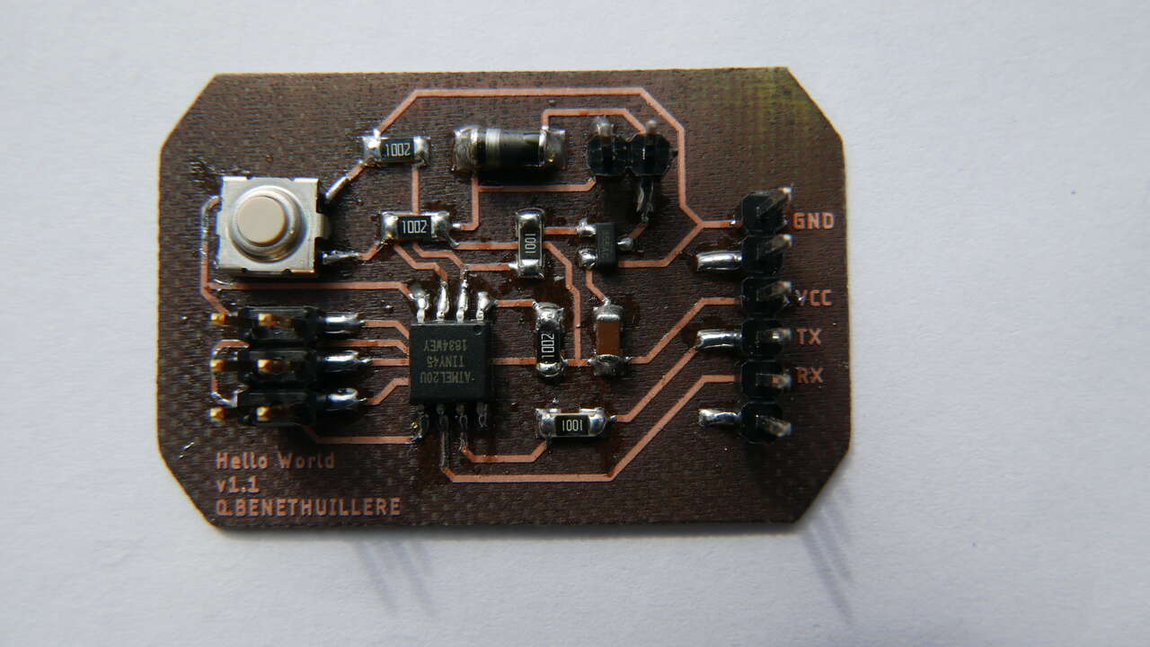 |
| Hello world + lock mechanism - board | Hello world + lock function - final PCB |
PCB design in Eagle
Designing a PCB was once again absolutely new to me. In order to do so I have used Fusion 360 dedicated free software called Eagle PCB. This software is specialized for designing PCB and for making electrical schematics. After an introduction from my fab instructor, I also ran into several tutorials : Eagle schematic, Eagle introduction tutorial, which by the way contained a very interesting link to understand the concept of pull-up / pull-down resistors.
Important things before starting working on the schematic was to download the Sparkfun, Adafruit and Fab libraries, and to activate them in Eagle. This allowed to access a wider range of electronics components in the software.
Schematic
First step was to create the electronic schematic for the circuit. As mentioned in the introduction, I have decided to add a functionnality to control a lock mechanism (electromagnet) via a push button. This implied adding a MOSFET, a diode a push button and several resistors (especially pull-up / pull-down resistors).
After a few iterations (especially on the components themselves), I came up with this final schematic :
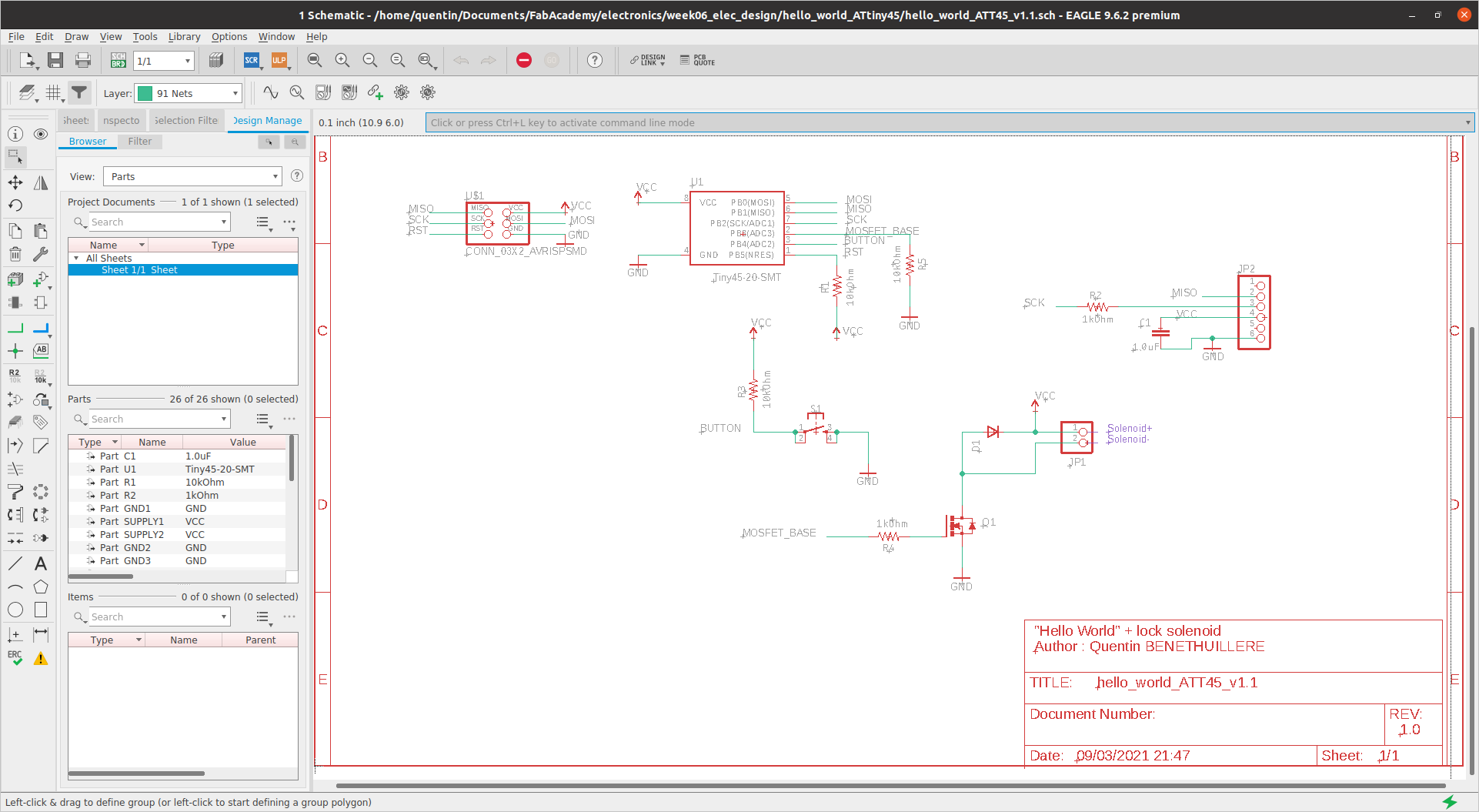
Hello world + lock mechanism schematic - Eagle
Board
Note : All the pictures in this section do not necessarily correspond to the final version of my work, but they are mainly here to present the workflow.
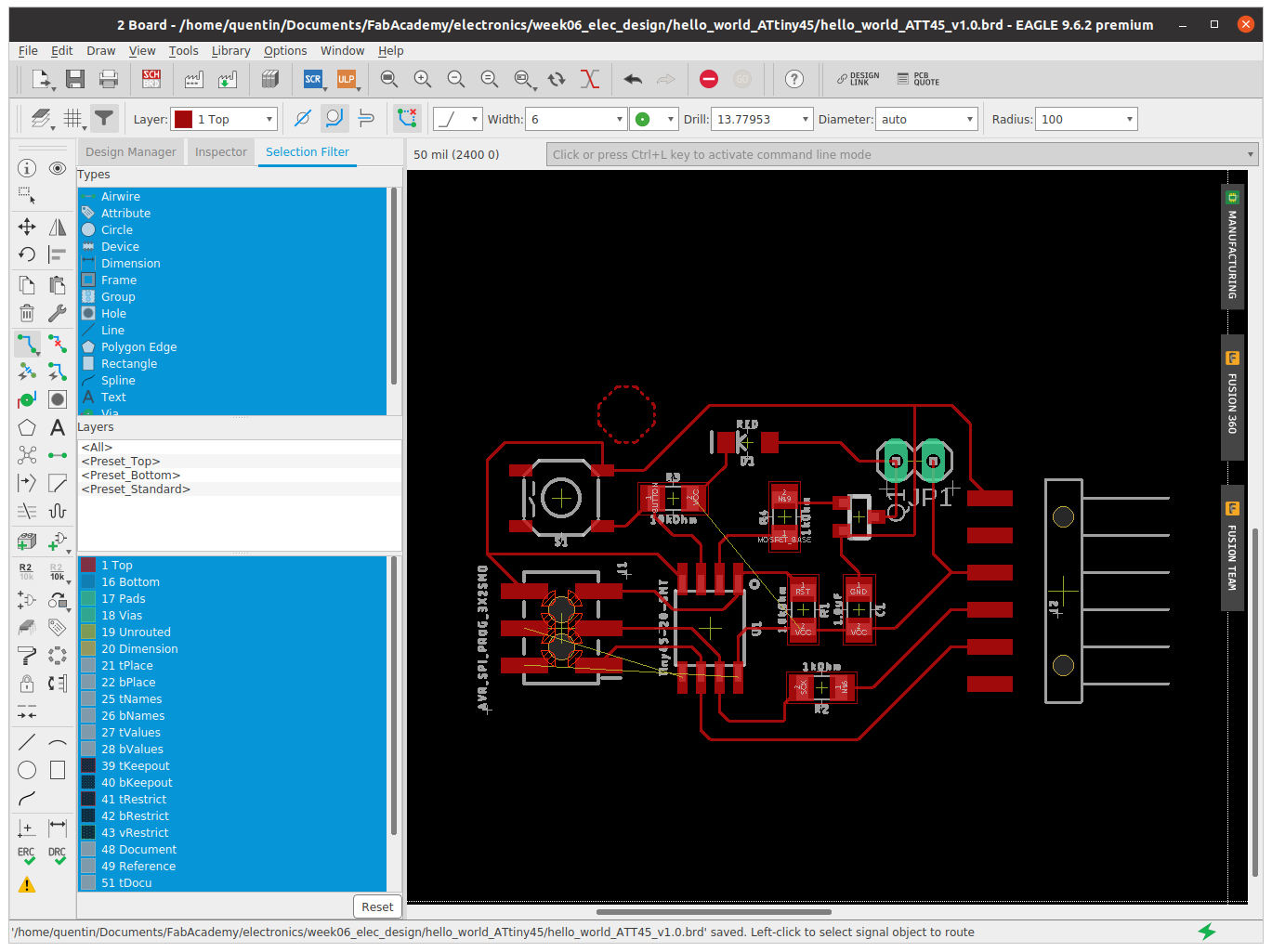
Once a first version of my schematic was ready, I could generate a corresponding version of a board in Eagle. At first, all the components were gathered in a corner of the board page connected with airwires according to the schematic (yellow lines in the image below).
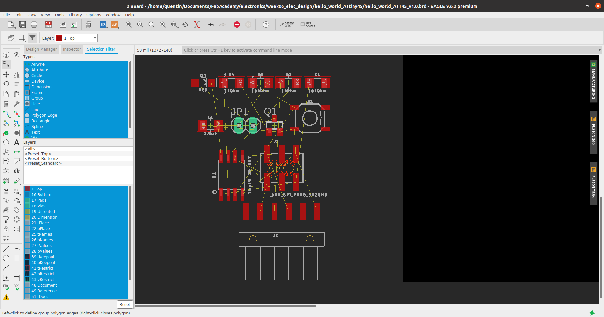
Eagle board generation
Then components had to be moved around :
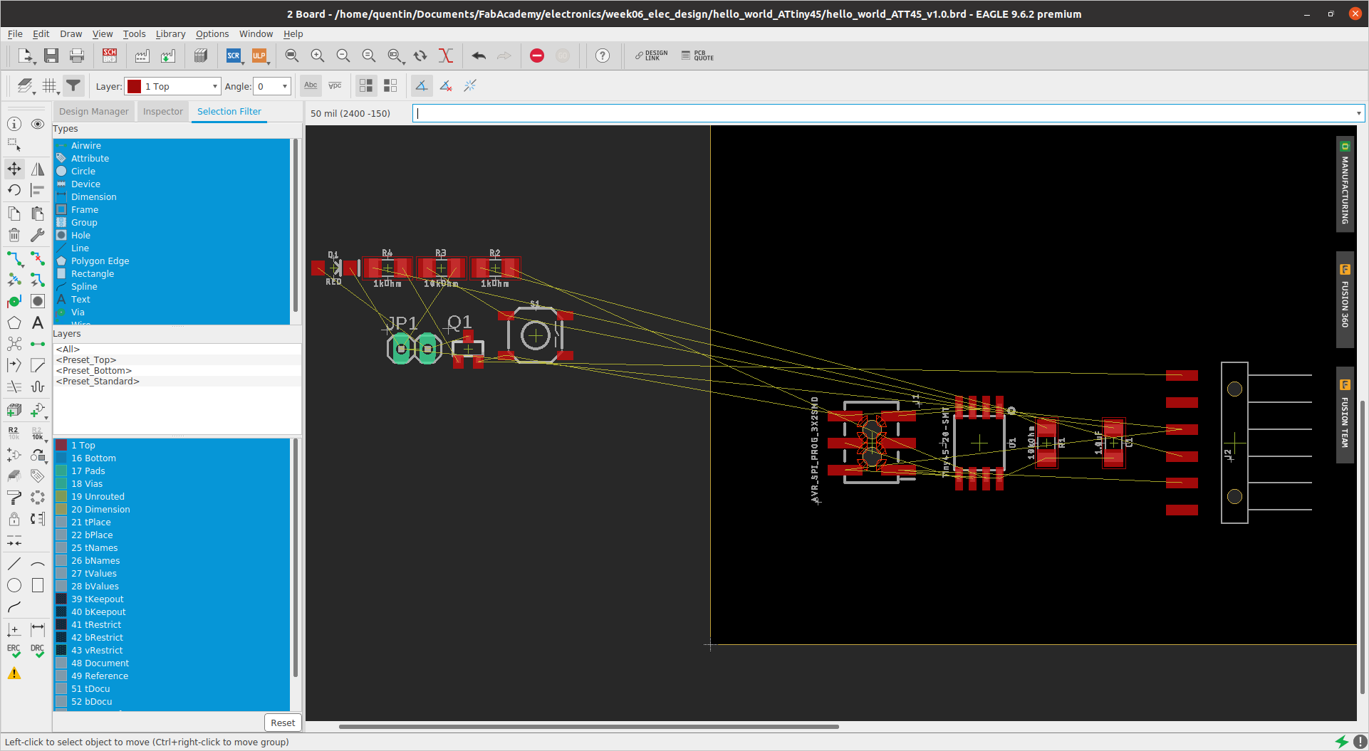 |
 |
| Board components arrangement - ongoing | Board components arrengement - completed |
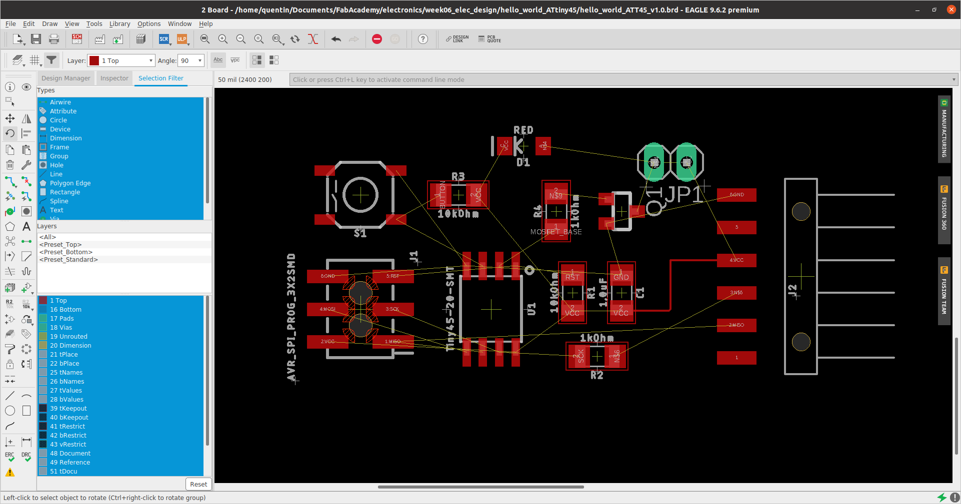
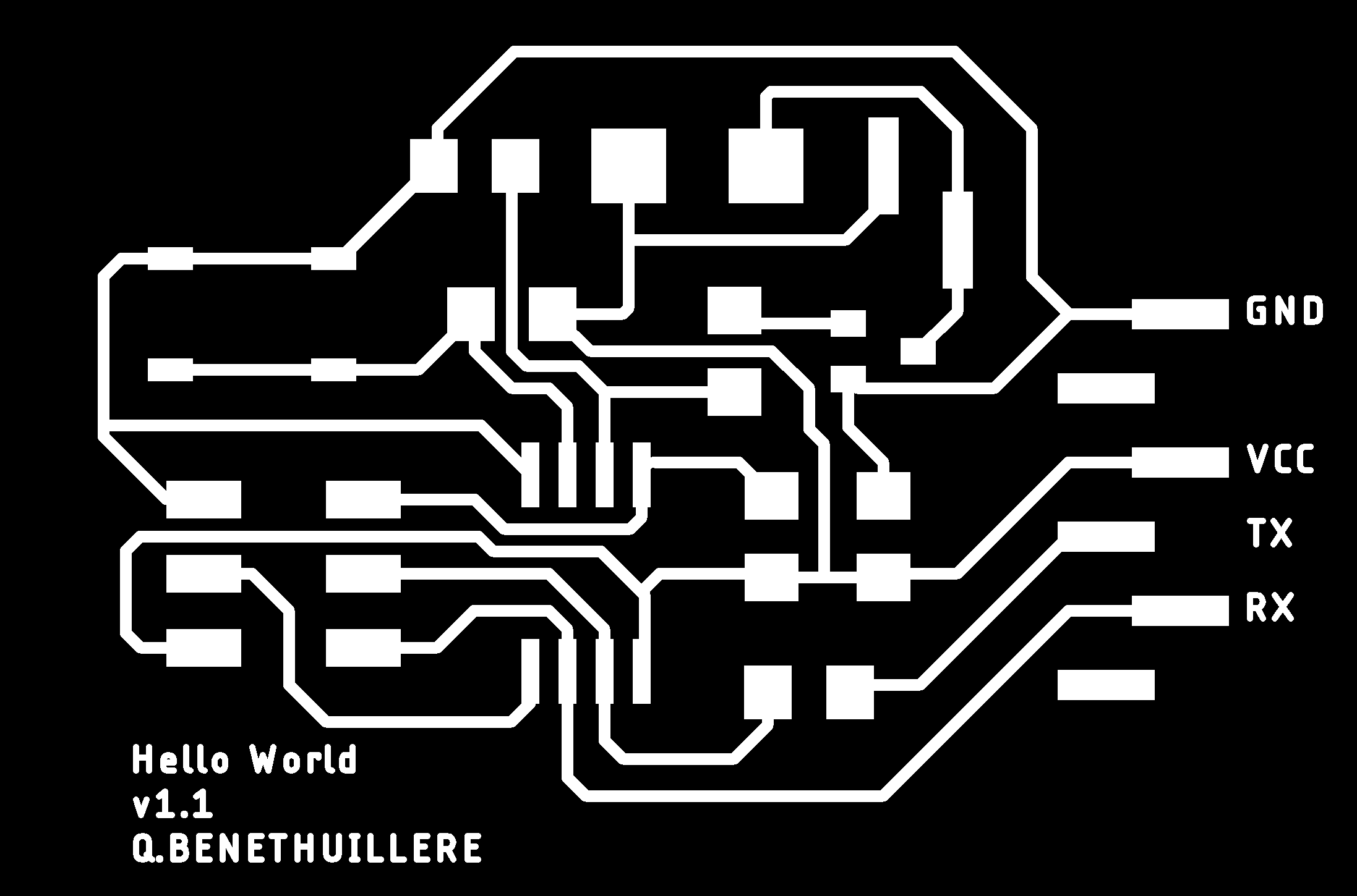
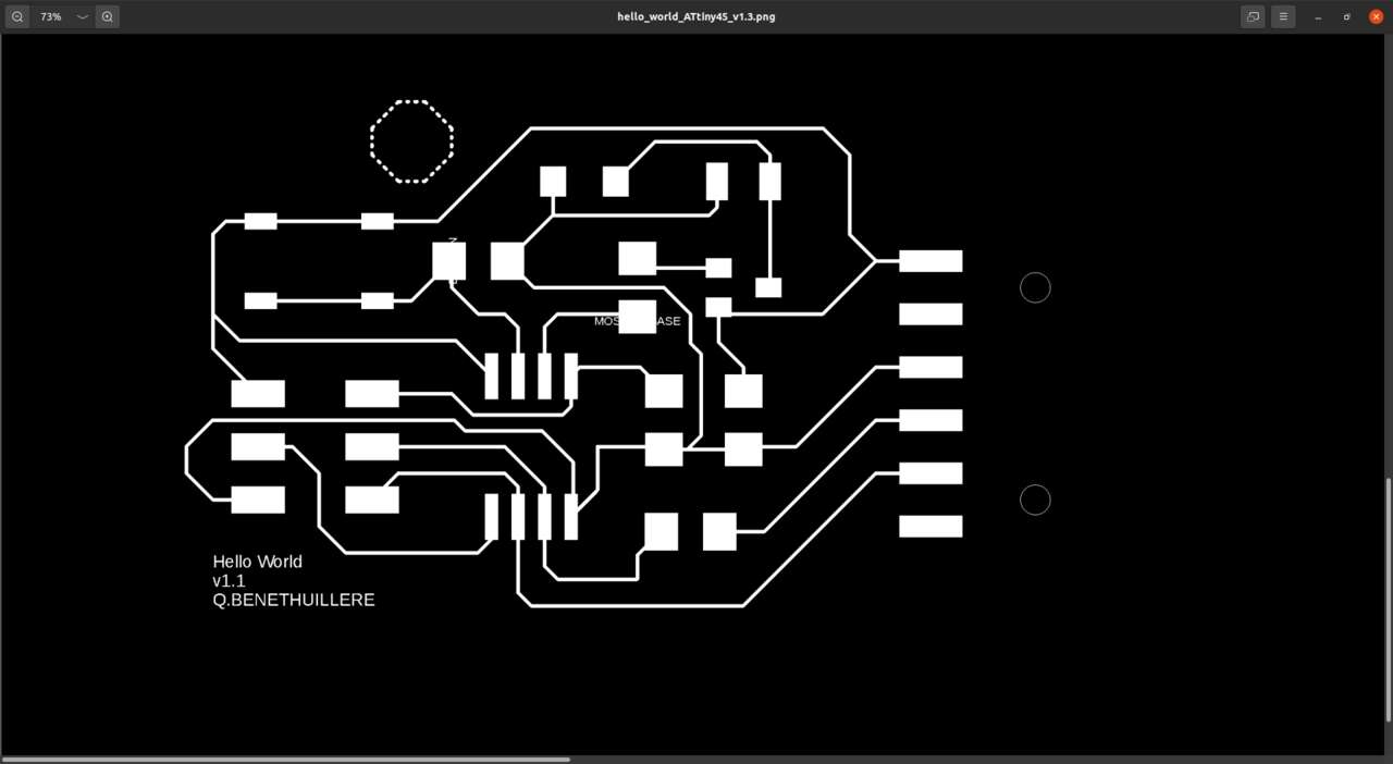
And finally I connected components with proper routes (replacing the airwires which are just there as indicators). Also added a Dimension layer that corresponds to the frame of my PCB. Below is the final version of the PCB I produced :
Hello world + lock function - board - Eagle
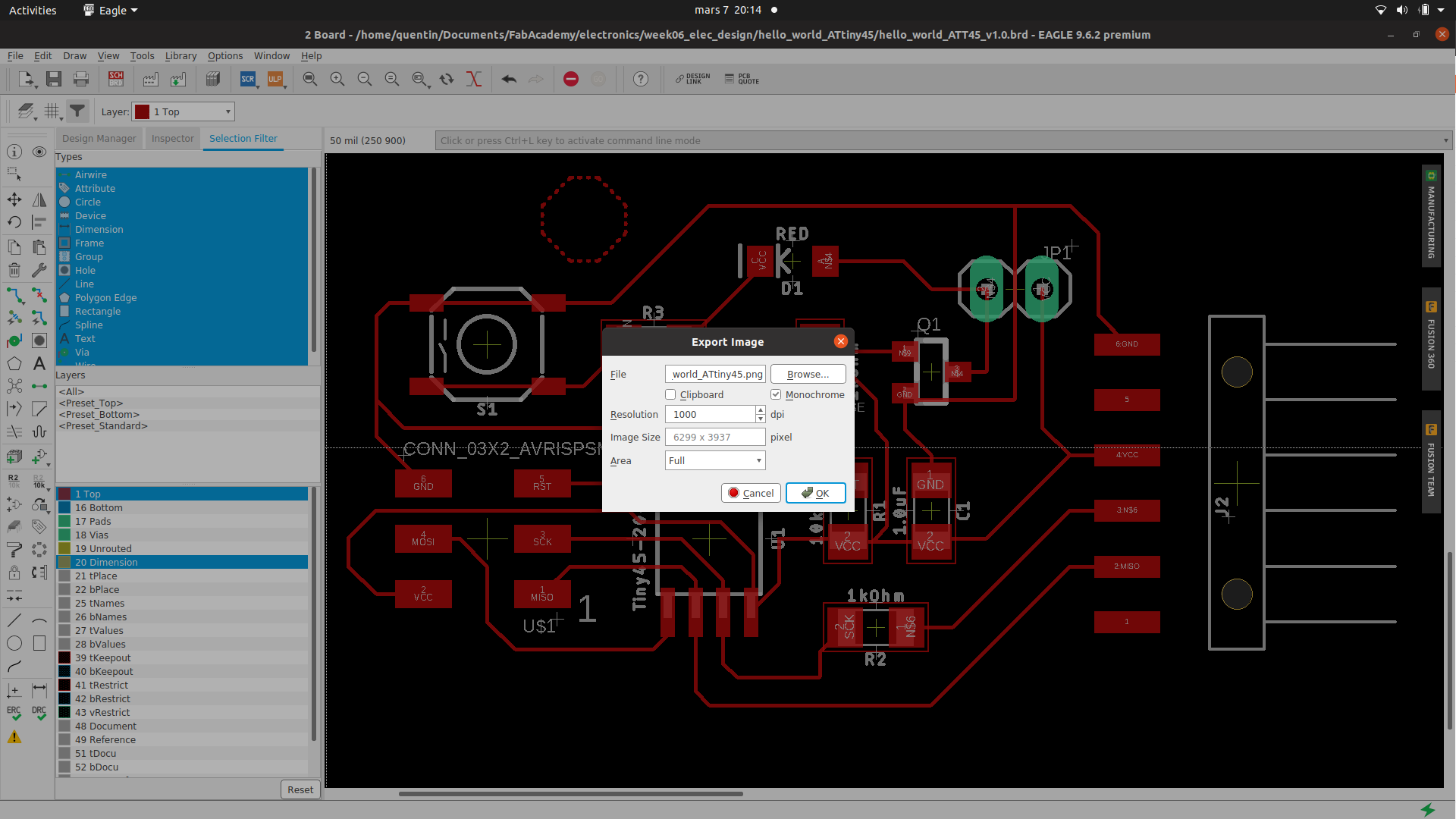
Export
Once the board was ready in Eagle, I could export it as .png files for the PCB production phase. For the export, I selected a high resolution (1000 or 1200), and chose monochrome. The export must be performed in 2 times :
- one export for the traces : only the Top layer must be visible.
- one export for the cutout : only the Dimension layer must be visible.
*** Note :*** To select the visible layers in Eagle Board window, in the top menu select “View -> Layer Settings”.
Eagle board export parameters
 |
 |
| Hello world board - traces export | Hello world board - cutout export |
Note : In order to be used for laser cutting, the cutout export must be inverted (black part of the image must become white and the other way around). This can easily be done in many image processing softwares such as Gimp (Colors → invert), Inkscape (Filters → Color → Invert), or even directly in CorelDraw (Transform → Invert).
Main issues
The main issues I faced were related to finding the appropriate components in Eagle libraries. There are thousands of them and it was not always easy to find the one I was looking for. And sometimes I even had to download other external libraries on the internet.
This particularly annoyed me when I was not able to route traces below my 2x3 ISP header (see the two remaining yellow airwires in the image below). It turned out that the problem vanished when I selected another 2x3 ISP header.
Incorrect ISP header
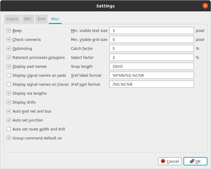
Also I had troubles with undesired white text appearing on my traces export. I fixed it by going to “Option -> Settings -> Misc tab”, and unselecting “Display signal names on pads” and “Display signal names on traces” (thanks Jonah Marrs for the tips).
 |
 |
| Text issue in traces export | Settings to fix the issue |
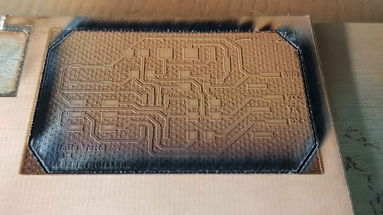
PCB production and soldering
In this section you will find pictures of the PCB production and soldering but you will not find any details because both topics have already been covered in the electronic production week.
On step I added compare to the electronic production week, was to first engrave my PCB on a piece of scrap wood with the laser cutter. The two main goals were to validate my engraving job prepared in CorelDraw sotfware, and also to make sure that the electronic components fitted correctly on my PCB. I judged this preparation work important given the difficulties encountered for finding the right components in Eagle.
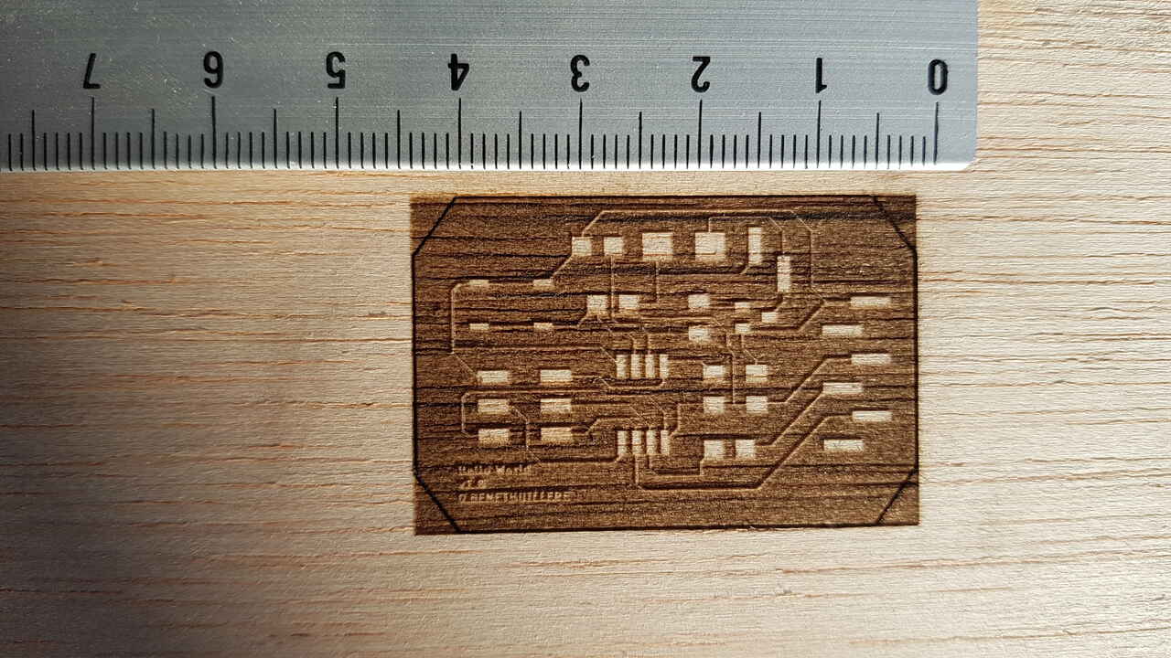
PCB engraved on wood
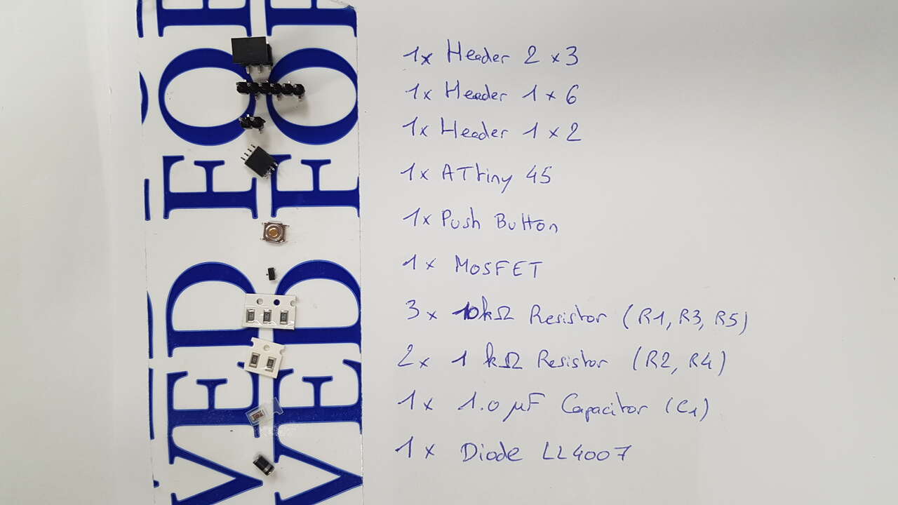 |
 |
| List of components | Verifying components size |
Based on the results observed, I have decided to increase the traces width to 0.40mm as I judged them too thin in this preparation work. I was afraid that they may break otherwise, and that they were not able to deliver enough current to the solenoid.
PCB production with laser cutter :
 |
 |
| Laser cut PCB - Traces | Laser cut PCB - Cutout |
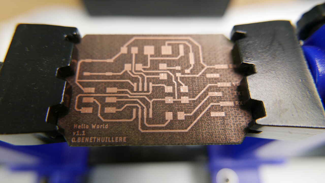
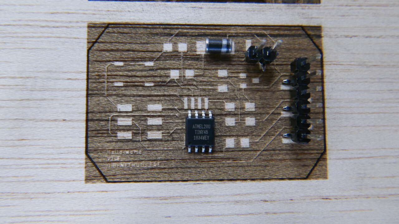
Hello world PCB before soldering
PCB soldering :
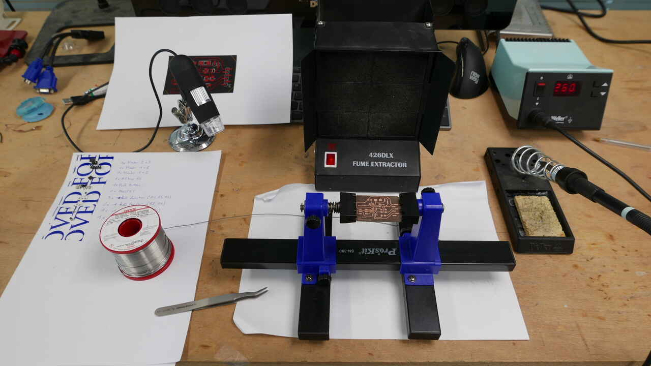 |
 |
| Soldering station | Soldering in progress |
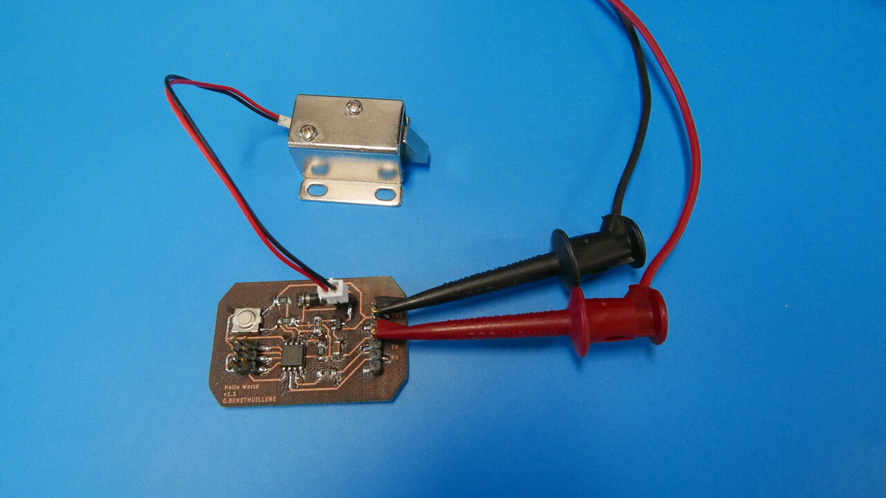
Hello world PCB final
Flashing SW
Basically my PCB supports the 2 following functionalities :
- serial communication.
- controlling a lock mechanism via a push button.
Ideally I should have made a program that allows using those 2 functionalities simultaneously. However, for simplicity purpose and lack of time, I have used a different program for each functionality.
In order to flash the programs on my microcontroller, I have used the FabTinyISP that I made during the electronic production week. My flashing setup is presented hereunder :
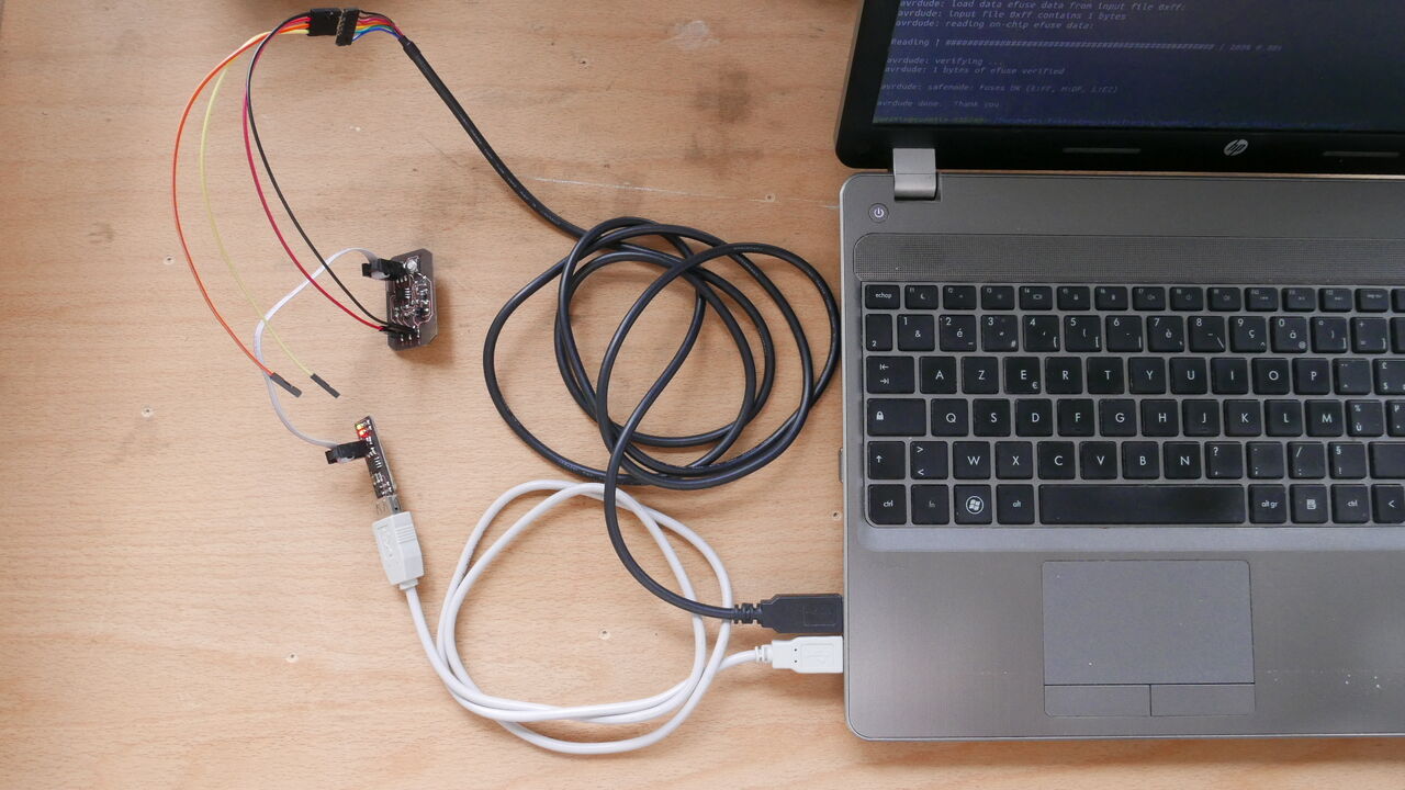
Flashing setup
Before being able to flash my programs, I had to generate the corresponding .hex files. This has been done using 2 different methods.
The source code for the hello world echo program was already provided in this FabAcademy page under the ATtiny45 section. I just had to generate the .hex file by running the following command :
sudo make -f ./hello.ftdi.45.echo.make
Note : The “-f” option (file) was necessary otherwise the C code was not compiled because other makefiles were present in the same folder I was working on, as shown in the screenshot below :
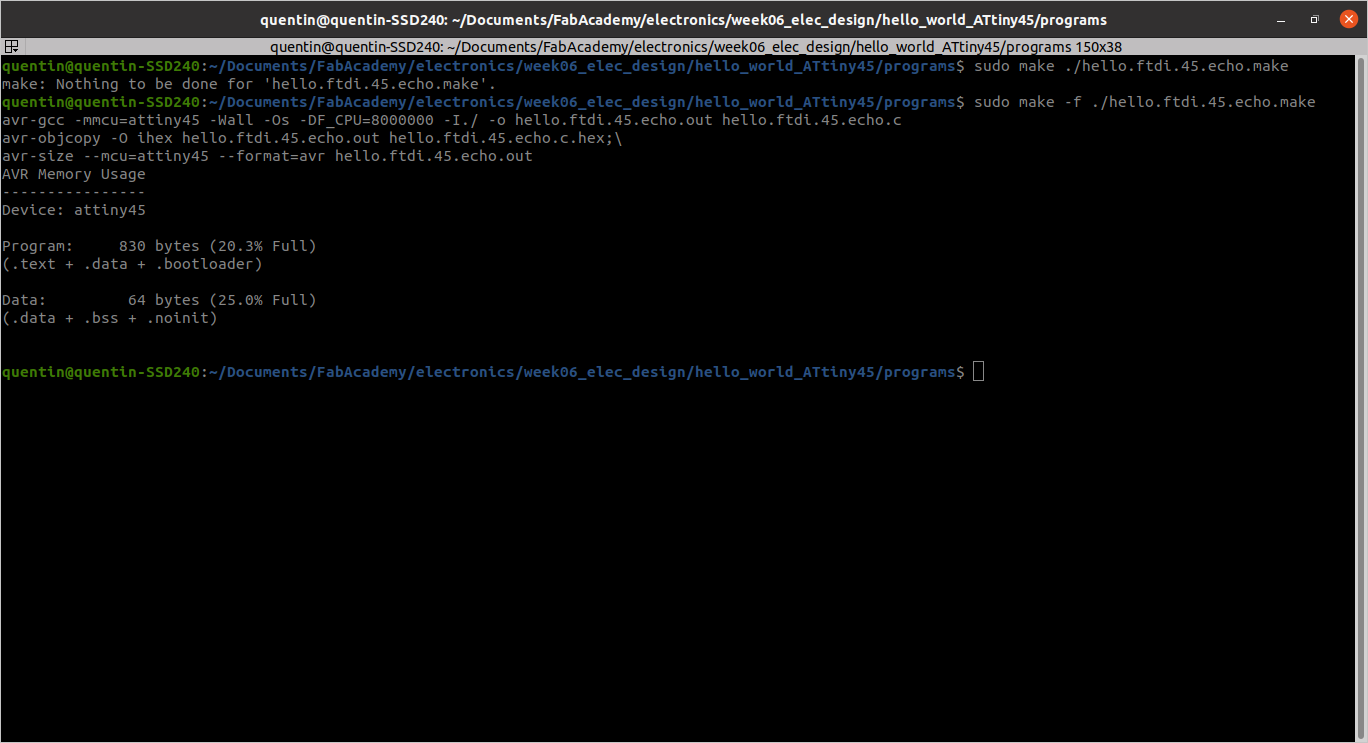
Generating the .hex file for the hello world echo program
As for the program to control the lock mechanism, I wrote the C code, and then compiled it using Atmel Studio software. This was the first time I was writing C code, and it was interesting to discover how to change bit values on the microcontroller. Here below is the C code I created.
#define F_CPU 8000000

#include <avr/io.h>

#include <util/delay.h>

// Button = PB4 = INPUT
// MOSFEFT base = PB3
// Button is open when 1, pushed when 0.

int main(void)
{
    DDRB = 0b11101111;

    while(1)
        {

        // Button pushed.
        if ((PINB & (1<<4)) == 0)
        {
        PORTB = PORTB | (1<<3)) ; // MOSFET base = 1
        _delay_ms(1000);
        }
        else
        {
        PORTB = PORTB & 0b11110111 ); // MOSFET base = 0
        _delay_ms(1000);
        }
    }

}
Once the .hex files were available I could flash them alternatively on my microcontroller using this command (by indicating the appropriate program name, and current serial port for my FabTiny ISP of course):
avrdude -c usbtiny -p t45 -P usb:002:031 -U flash:w:hello.ftdi.45.echo.c.hex
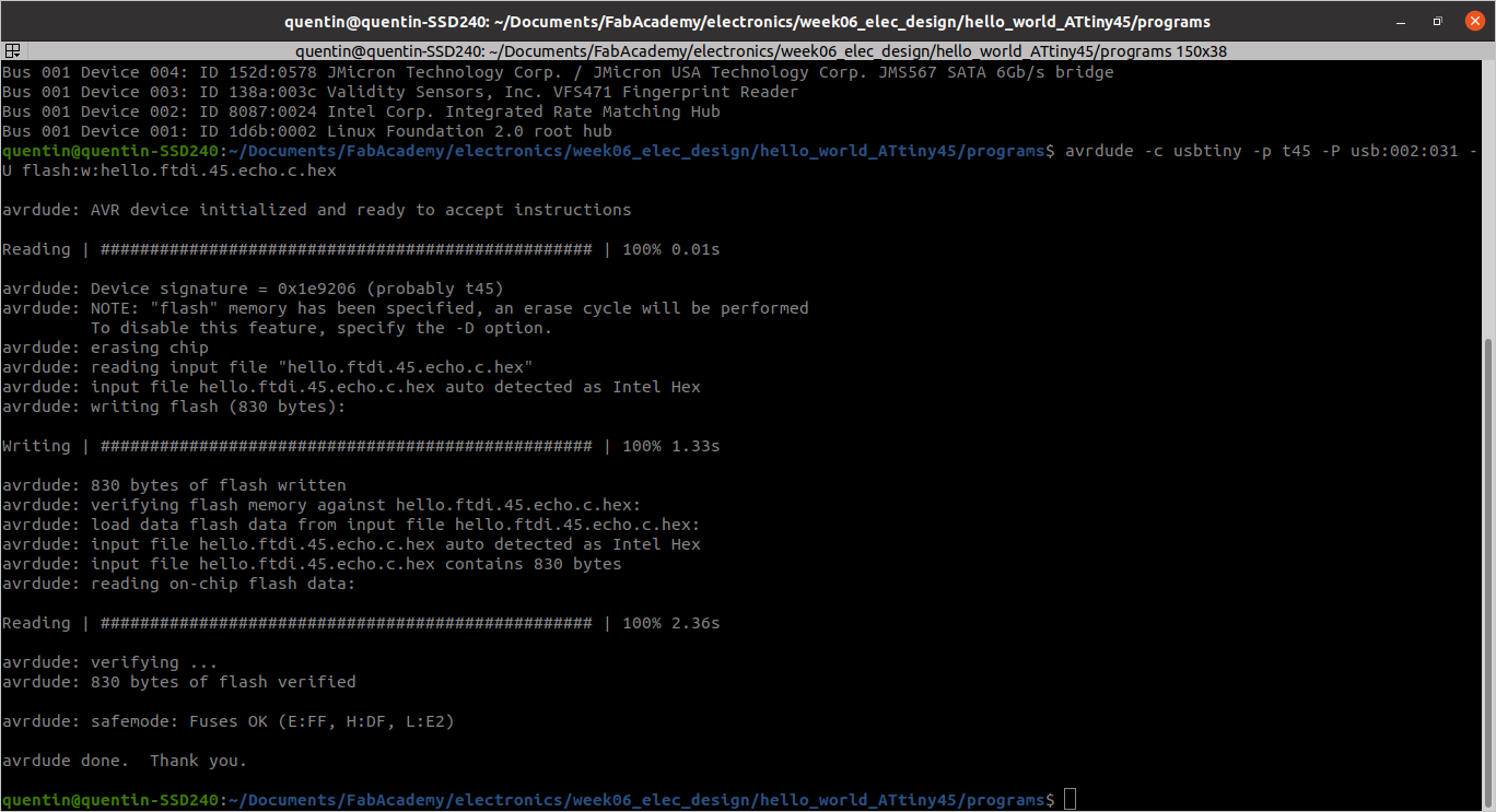
Flashing hello world echo program
And last step was to set the fuses to the desired value. Fuses basically determine the behaviour of the microcontroller. Those information are saved in a non-volatile memory as 3 bytes : “fuse low” (lfuse), “fuse high” (hfuse) and “fuse extended” (efuse). These bytes can be reprogrammed as many times as desired. For further information on fuses, refer to this website.
In my case I just wanted to modify one bit compare to default values so that the clock is not divided by 8 in the microcontroller. In order to get the appropriate command I used the AVR fuse calculator website.
avrdude -c usbtiny -p t45 -P usb:002:013 -U lfuse:w:0xe2:m -U hfuse:w:0xdf:m -U efuse:w:0xff:m
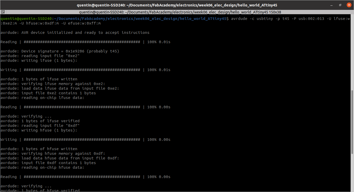
Setting the fuses
If I would have liked to keep the default values for the fuse configuration (with the clock divided by 8 in the microcontroller) I would have had used the following command instead :
avrdude -c usbtiny -p t45 -P usb:002:013 -U lfuse:w:0x62:m -U hfuse:w:0xdf:m -U efuse:w:0xff:m
Testing
Lock mechanism
Before testing the complete lock mechanism using the push button, I did a simple test by flashing an other program on my microcontroller. This program was basically just setting alternatively all the pins of the microcontroller to 1 or 0, given a certain timing. By connecting a LED into my PCB instead of the lock mechanism solenoid, I could see the LED blinking as expected.
LED blink test setup
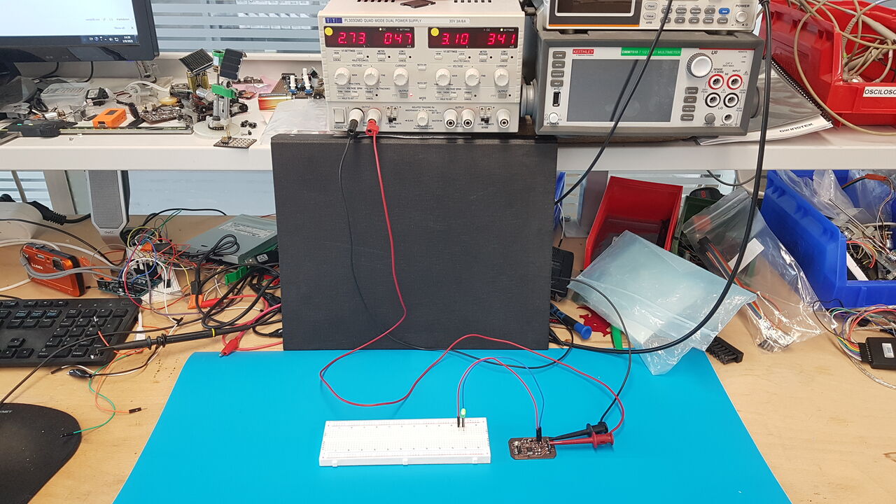
Then I replaced the LED by the solenoid, increased the maximum current the power supply could deliver (because from all I read on the solenoid it was expected to request at least 500mA to operate), and I could see that my lock mechanism was opening and closing alternatively as expected.
Lock mechanism test setup
And finally I repeated those LED and lock mechanism tests with the program I generated that controls the LED/solenoid output based on the push button state. This was a success, and the result is presented in the video below :
Note : The short delay we can observe in the video between the push button press/release and the lock mechanism state change is due to simple 1 seconde delays I added in my C code to avoid button boucing issues. This should definitely be handled in a more apropriate way but this was not the purpose of my tests here.
Hello world
As for testing the serial communication between my PCB and my computer, I have used the serial communication interface provided in the Arduino IDE. Also it was important for this test to connect the Rx and Tx pins of my PCB to the cable connected to my computer over USB.
First I opened the serial communication interface by clicking on the button highlighted in the image below :
Arduino_IDE_highlight
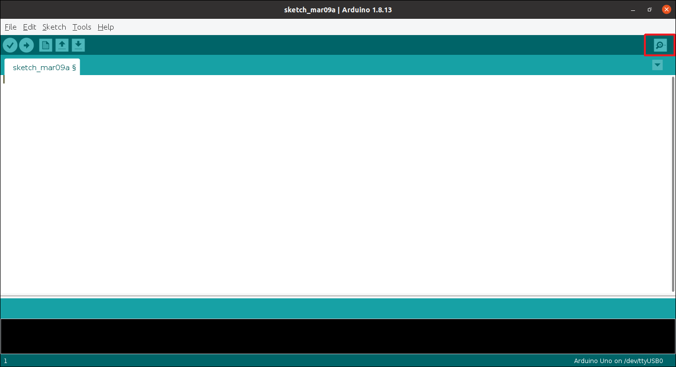
Serial communication button - Arduino IDE
And after that I made sure that the baudrate was set to 9600, I could send input text to the interface and observe the echo from the PCB. The Hello World was working !
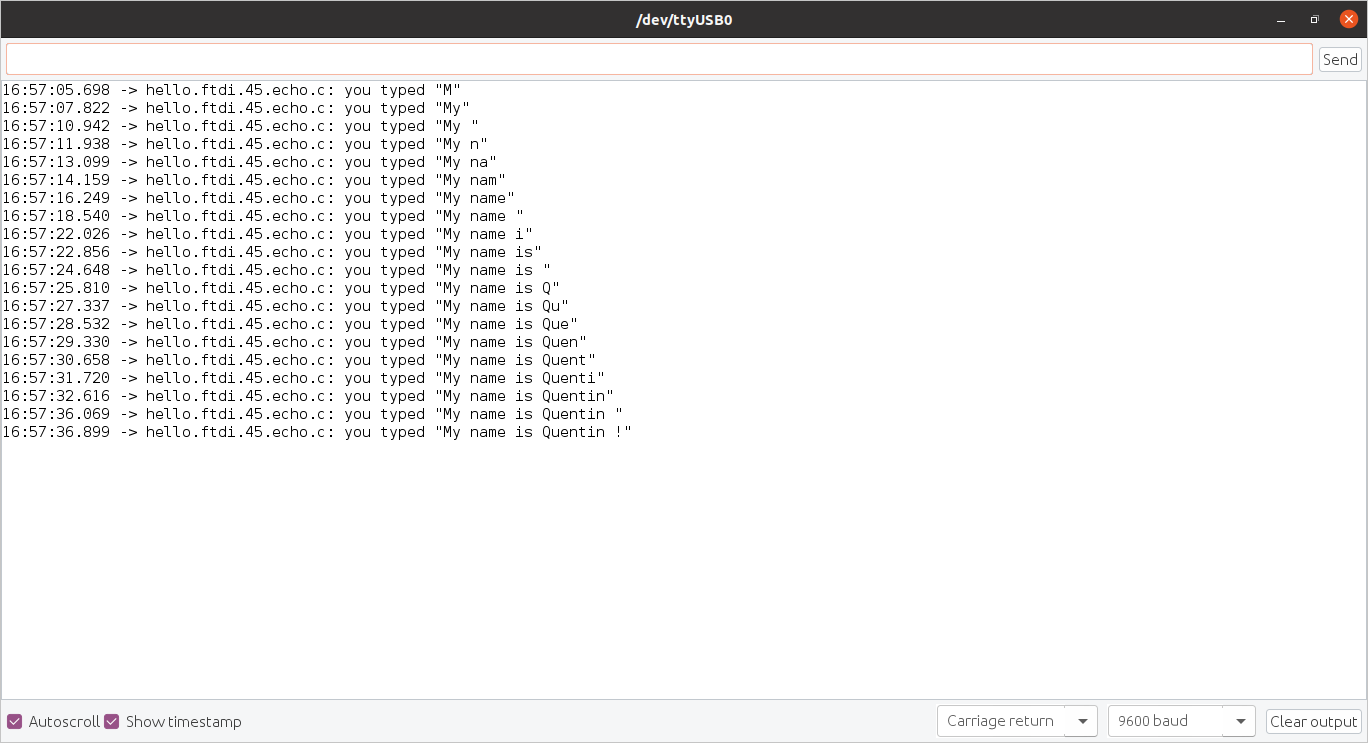
Hello world echo test
This test concluded successfully this electronics design week.
Group Assignment
Our lab instructor gave us an introduction on how to use an oscilloscope, a signal generator and a logic analyzer. Here below is the material available at Fablab Disgiscope :
- Oscilloscope DSO-X-2014A
- Signal generator GW Instek AFG-2015
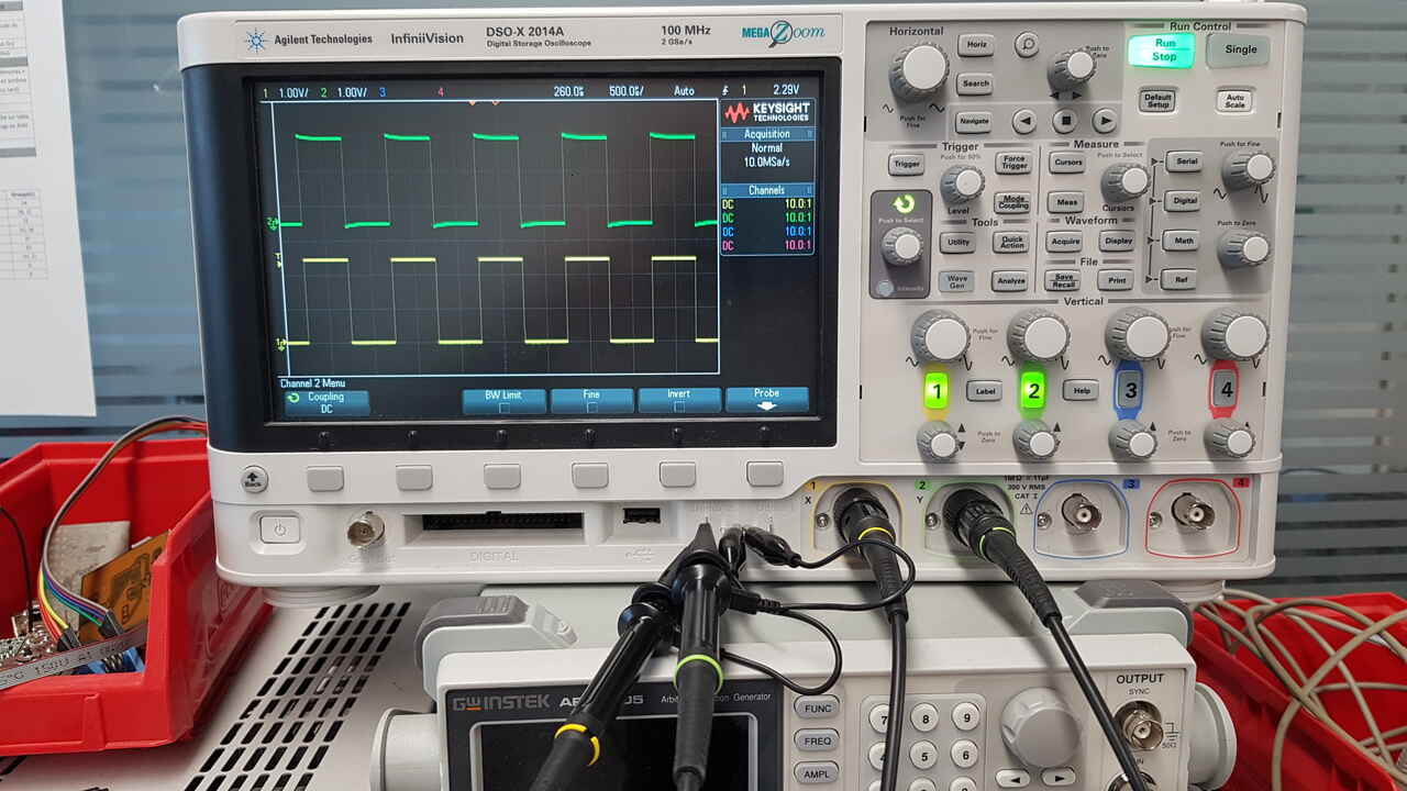
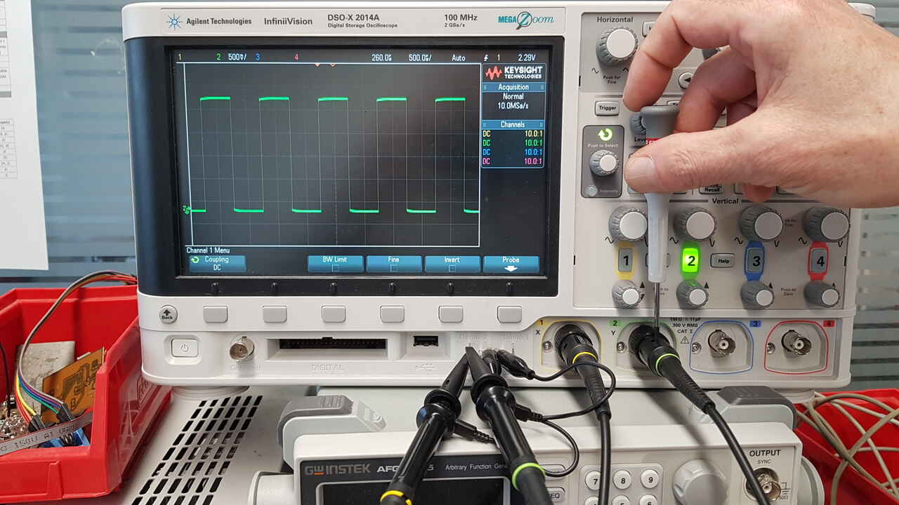
Using the demo mode of the oscilloscope, we could for example observe that one of the probe was not correctly calibrated (green signal in the image below). This could then be fixed by screwing/unscrewing the dedicated calibration element on the probe.
 |
 |
| Oscilloscope demo mode | Probe calibration |
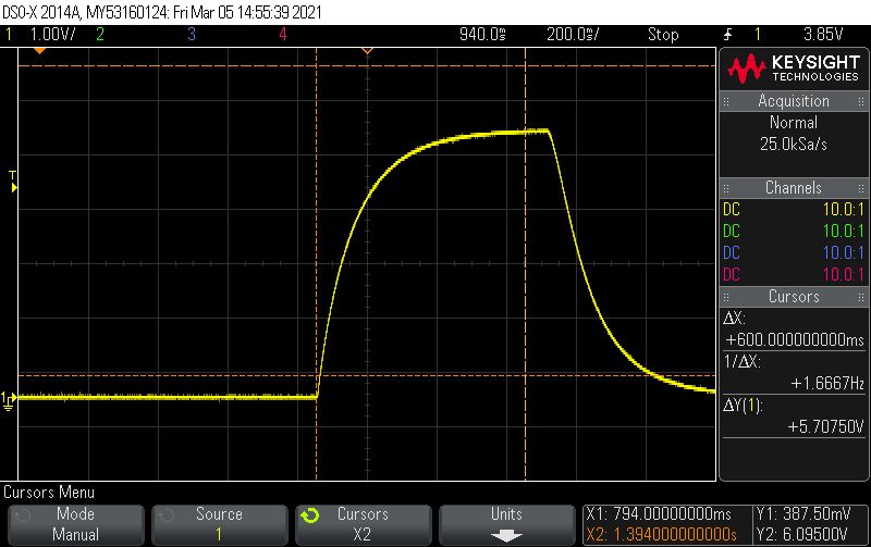
We also observed the charge and discharge of a capacitor with the oscilloscope :
 |
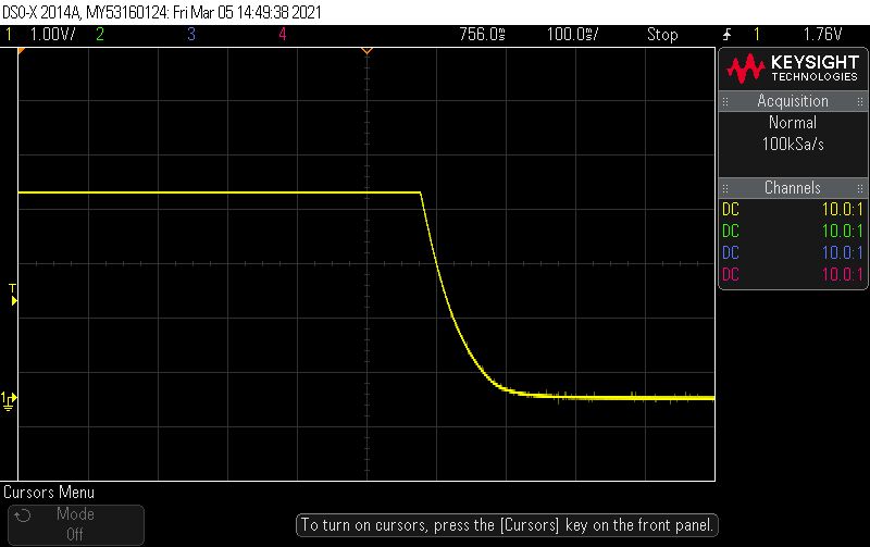 |
| Capacitor charge | Capacitor discharge |
And finally got introduced to the logic analyzer EasyLogicAnalyzer and its dedicated software to observe signals variation. We measured here only one signal but this tools allows to track up to 16 signals at the same time, which is very convenient when dealing with communication protocols. We will definitely need to use it later in this course. Unlike the oscilloscope, the logic analyzer only treats signals as 0 or 1, and cannot render transient states as the oscilloscope.
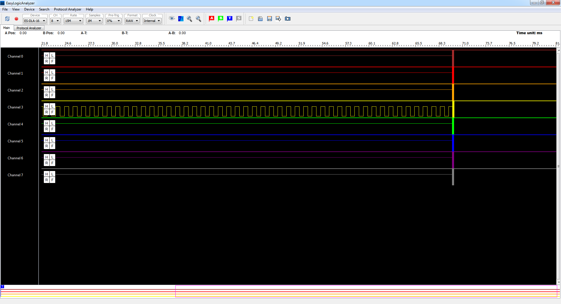
Logic analyzer
Source files
The source files of the work presented in this week assignment are available for download here :