4. Electronics production
Assignments:
Individual assignments:
- Make an in-circuit programmer by milling and stuffing the PCB.
- Test it.
- Optionally, try other PCB processes.
Group assignment:
- Characterize the design rules for your PCB production process.
Building a FabTinyISP
Introduction
For this electronics production week, the main goals were to get familiar with one or several process(es) for making an electronic PCB (Printed Circuit Board), soldering, and troubleshooting any potential issue. In order to do so, I have followed my lab instructor proposal to build a FabTinyISP, which is an ISP programmer (In-System Programming). This eletronic circuit board will then allow me to program microcontrollers that are already fitted on an electronic circuit, which will definitely be helpful for the rest of the program.
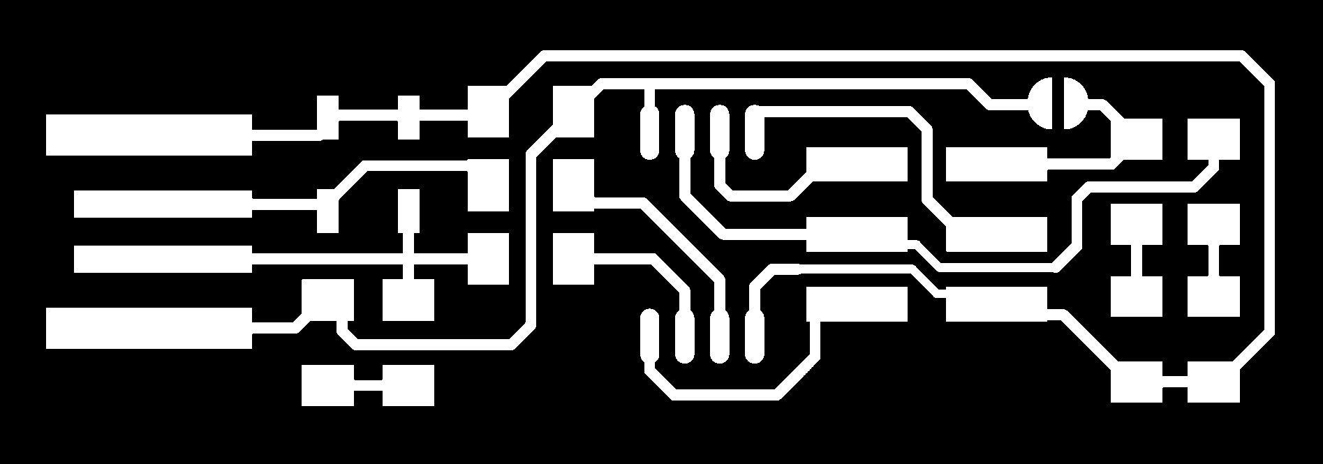
The complete methodology that I have been through is described in this tutorial. This is a one side circuit as can be seen in the electronic design below (already provided in the tutorial) :
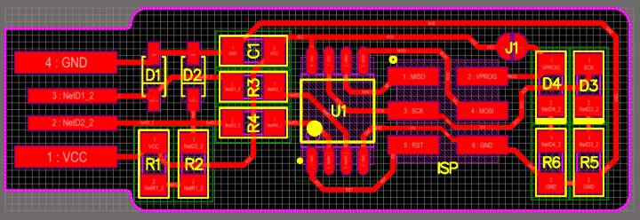
PCB electronic design traces
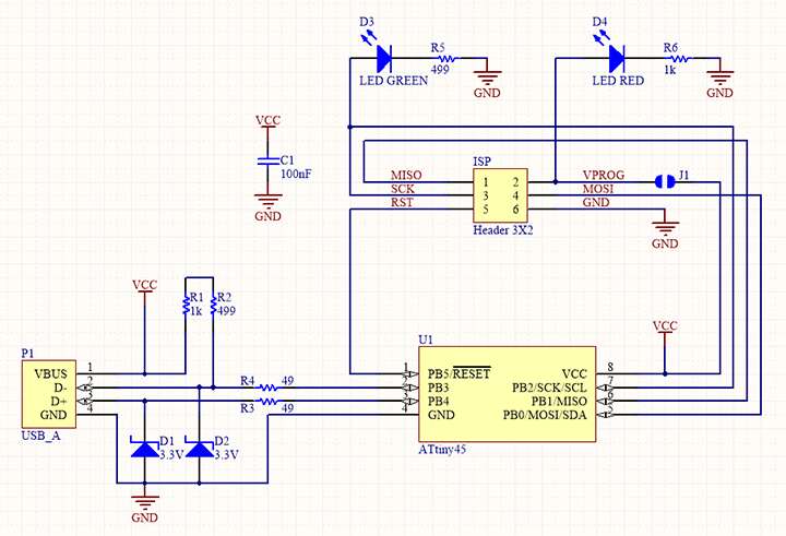
PCB electronic design schematic
Making the PCB
Instead of milling the PCB, it has been decided in my lab that we would rather laser cut it. The reasons for this choice are the following :
- Better resolution achievable.
- No mechanical parts gets damaged such as drill bits used in the milling process.
- No need to cut holes because it is a one side circuit.
- Less noisy.
- Laser cutting technics have already been adressed in the program, which is not yet the case for milling.
The material used was an FR4 epoxy fiber glass plate covered with a layer of copper (see pictures in the description of the process).
Here is the workflow I followed for getting my PCB ready.
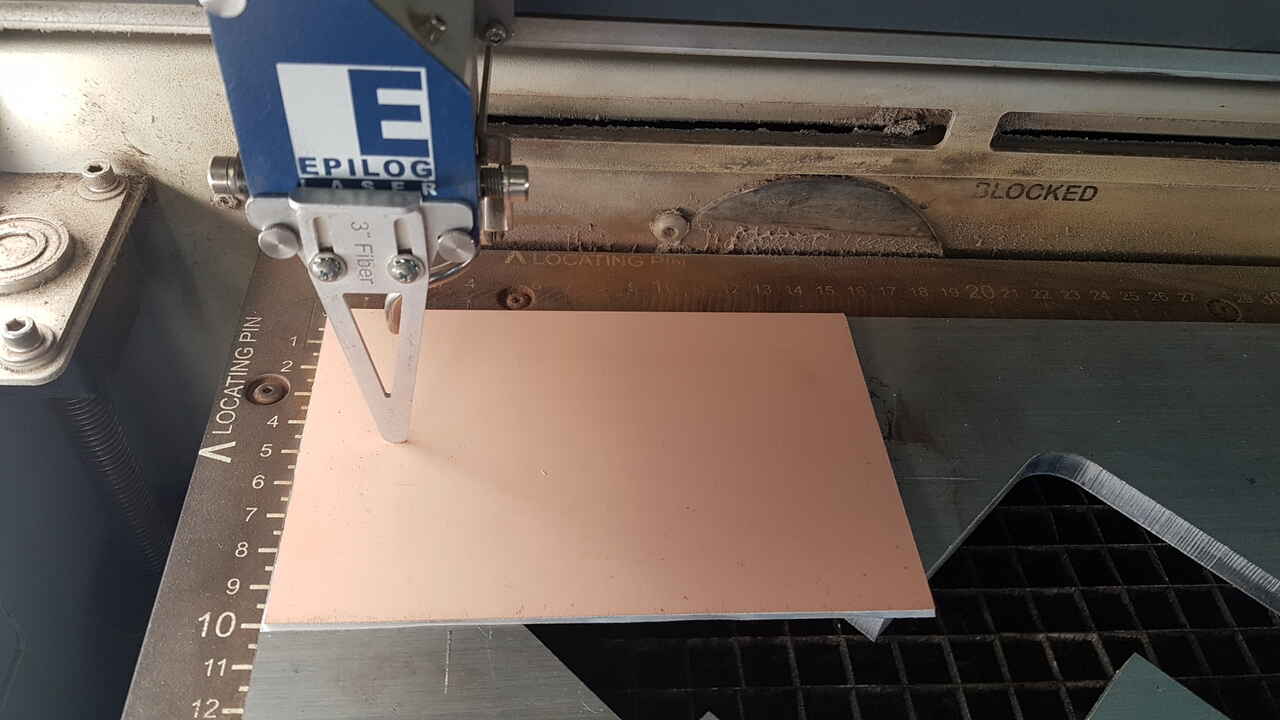
1 - Taped the FR4 plate on a flat mettalic wider plate (using double-sided tape). The idea is to make sure that the plate to be laser cut does not move during the engraving and cutting process as a high precision is required. Also, note that due to the very short focal of the fiber laser, the surface must absolutely be flat otherwise the engraving quality may be considerably altered.
2 - Adjusted the laser cutter plate height, and prepared the job to be executed in CorelDraw software.
Adjusting laser cutting height
Note : The cutting had to be done in two phases :
- The first phase consisted in removing the copper where not needed (basically everywhere that is not an electronic trail or pad).
- The second phase consisted in cutting the PCB out of the main FR4 plate.
First phase was executed using the fiber laser (for metal cutting), whereas the second phase was performed with the CO2 laser (cutting the epoxy fiber glass layer).
As for facilitating the job preparation, the “layer” option has been used in CorelDraw to clearly separate both phases; see screenshot below.
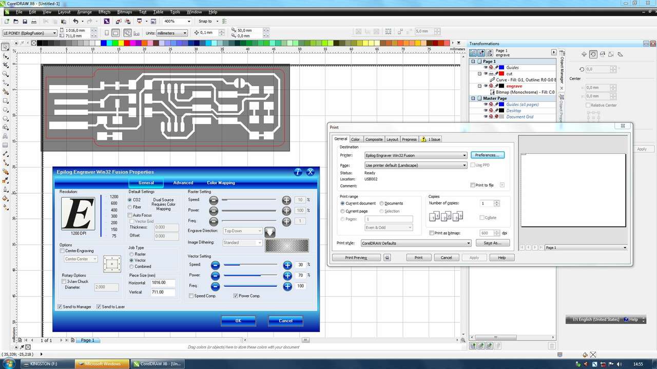
CorelDraw - laser cut job preparation
Note : The cicruit traces and frame cutout were already provided in the turotial as .png files :
 |
 |
| FabTinyISP - Traces | FabTinyISP - Cut out |
3 - Executed first phase of the job : removal of the copper layer where undesired.
Laser settings used :
- type : fiber
- speed : 10%
- power : 100%
- frequency : 1
- repetition : 1
Before continuing to the next step, I checked that the copper layer had been removed sufficiently by performing some continuity tests with a multimeter. Had I observed some issues, I would have had restarted a job to make sure that the whole layer of copper had vanished.
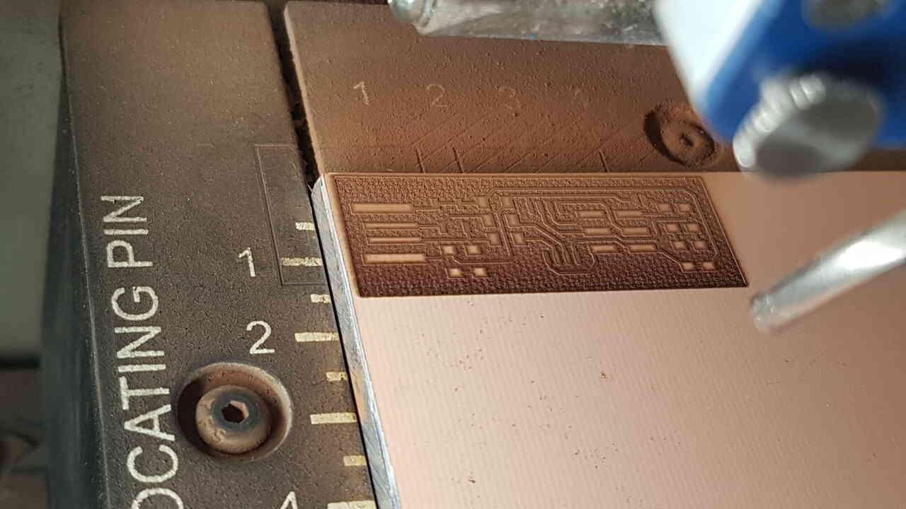
PCB after laser cutting undesired copper
4 - Executed second phase of the job : cutting out the PCB from the main plate.
Laser settings used :
- type : CO2
- speed : 30%
- power : 70%
- frequency : 100
- repetition : 15
Note : The video presented above does not show the 15 repetitions, but it is important to mention that the flame produced when cutting the epoxy fiber glass layer becomes less and less intense as there is fewer material left, which is a good indication to know when the laser has cut through the material.
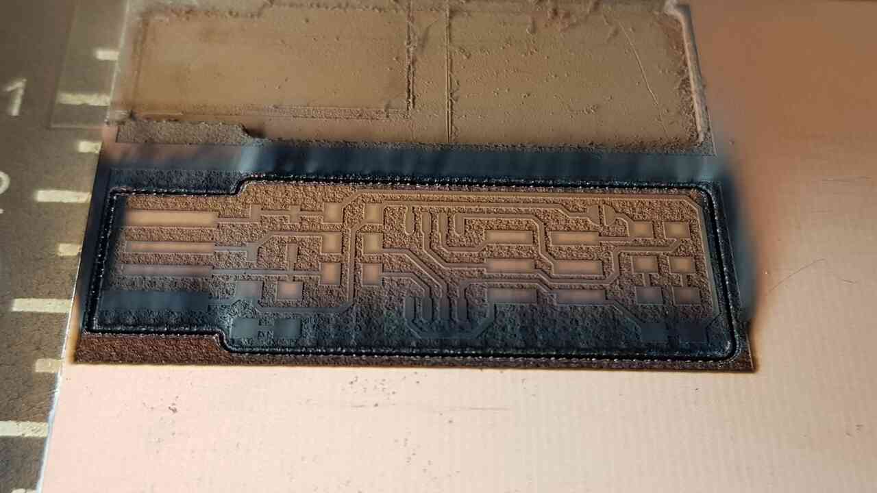
PCB after laser cutting frame
Once the cut finished, one can see that the PCB appeared as burnt, but it was not as will be seen in next step.
5 - Cleaned the PCB with isopropyl alcohol which made it become bright and shiny.
Cleaning PCB
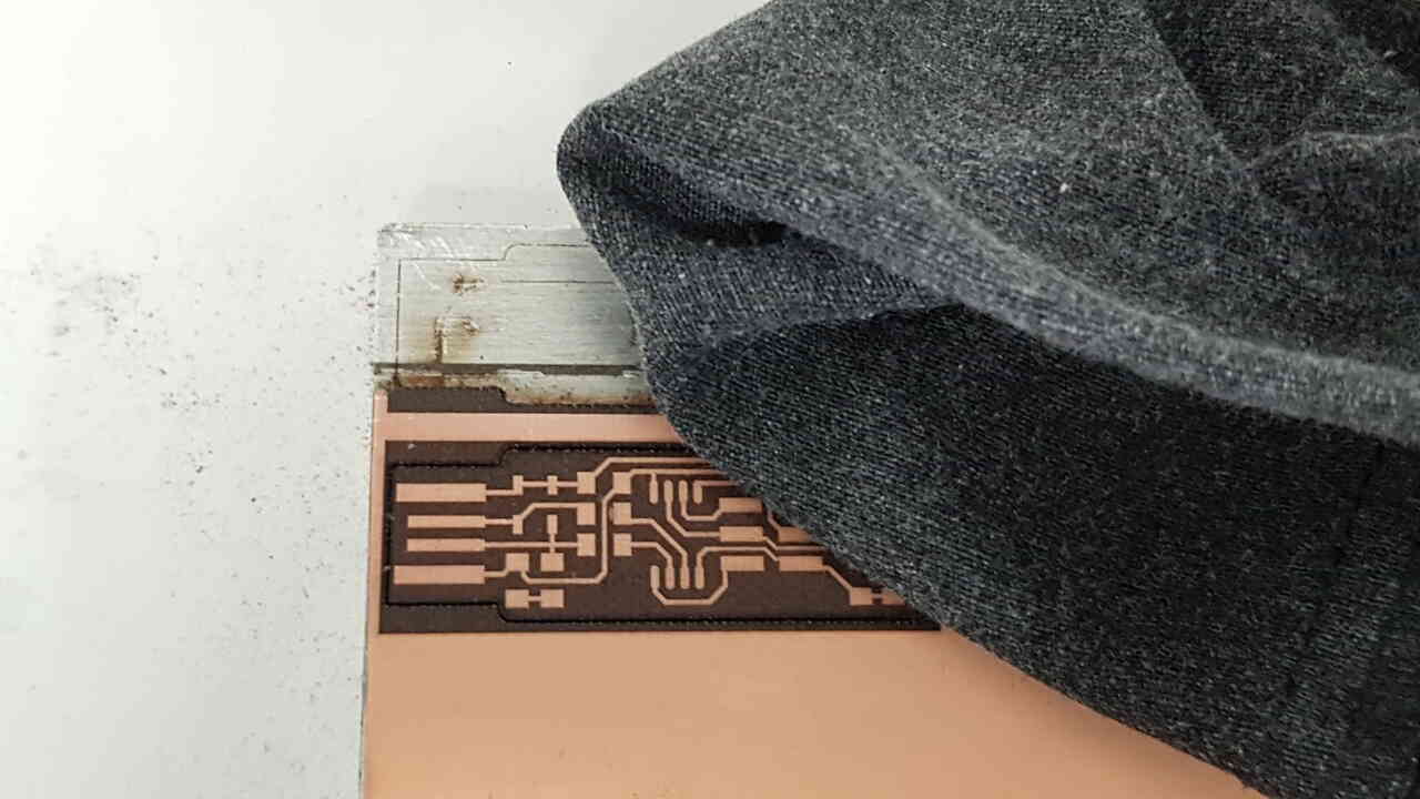
6 - Removed the PCB from the main plate using a palette knife, and removed the tape underneath it.
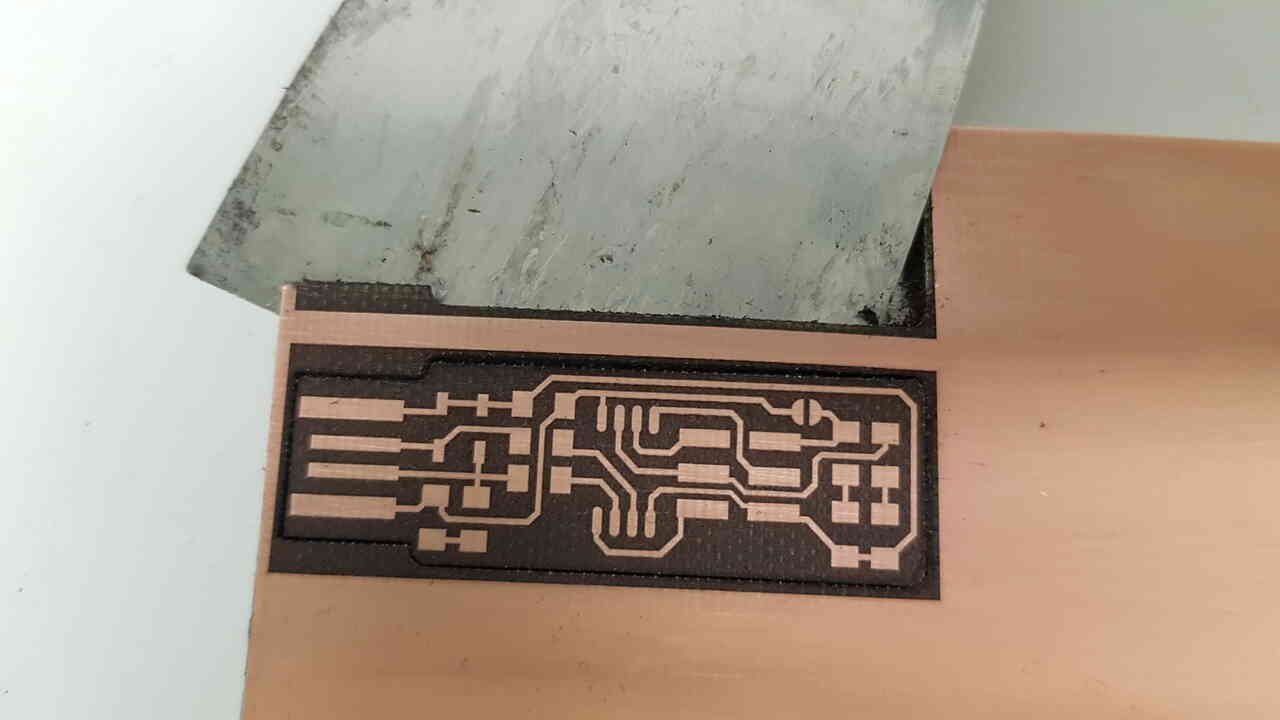
Extracting PCB with palette knife
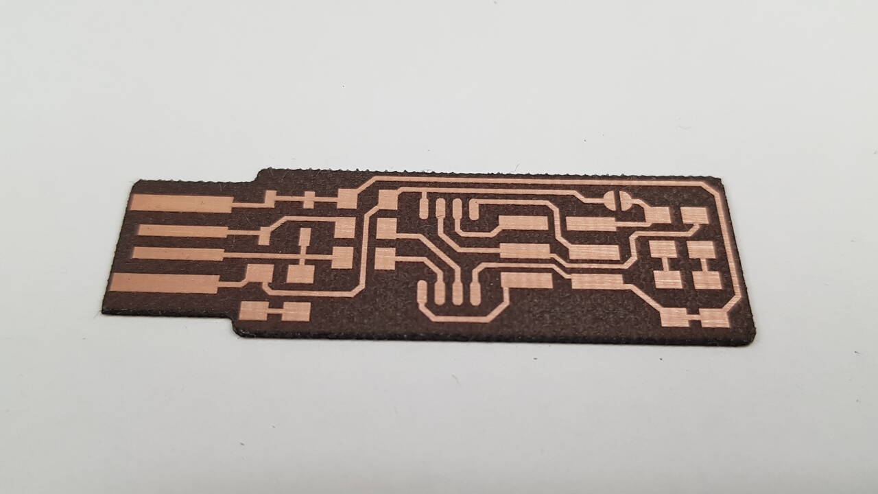
PCB front side
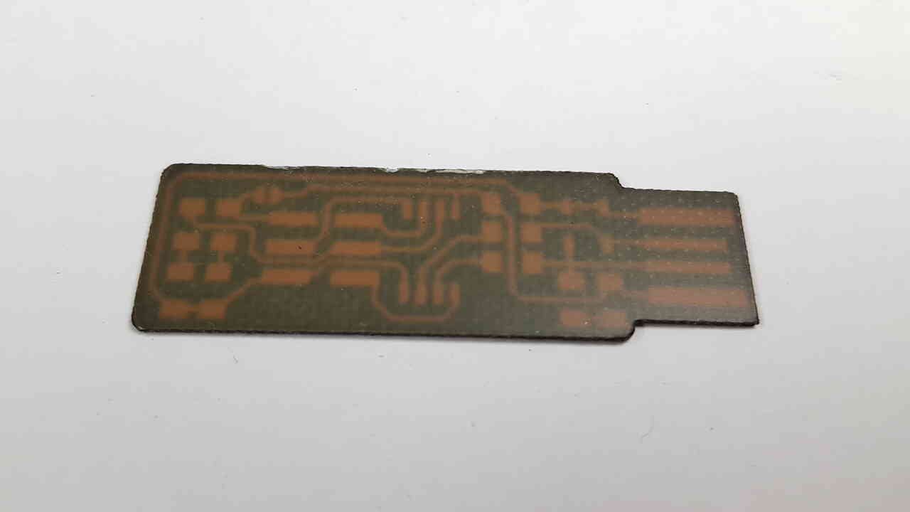
PCB back side
7 - Visually inspected the PCB tracks using an electronic microscope.
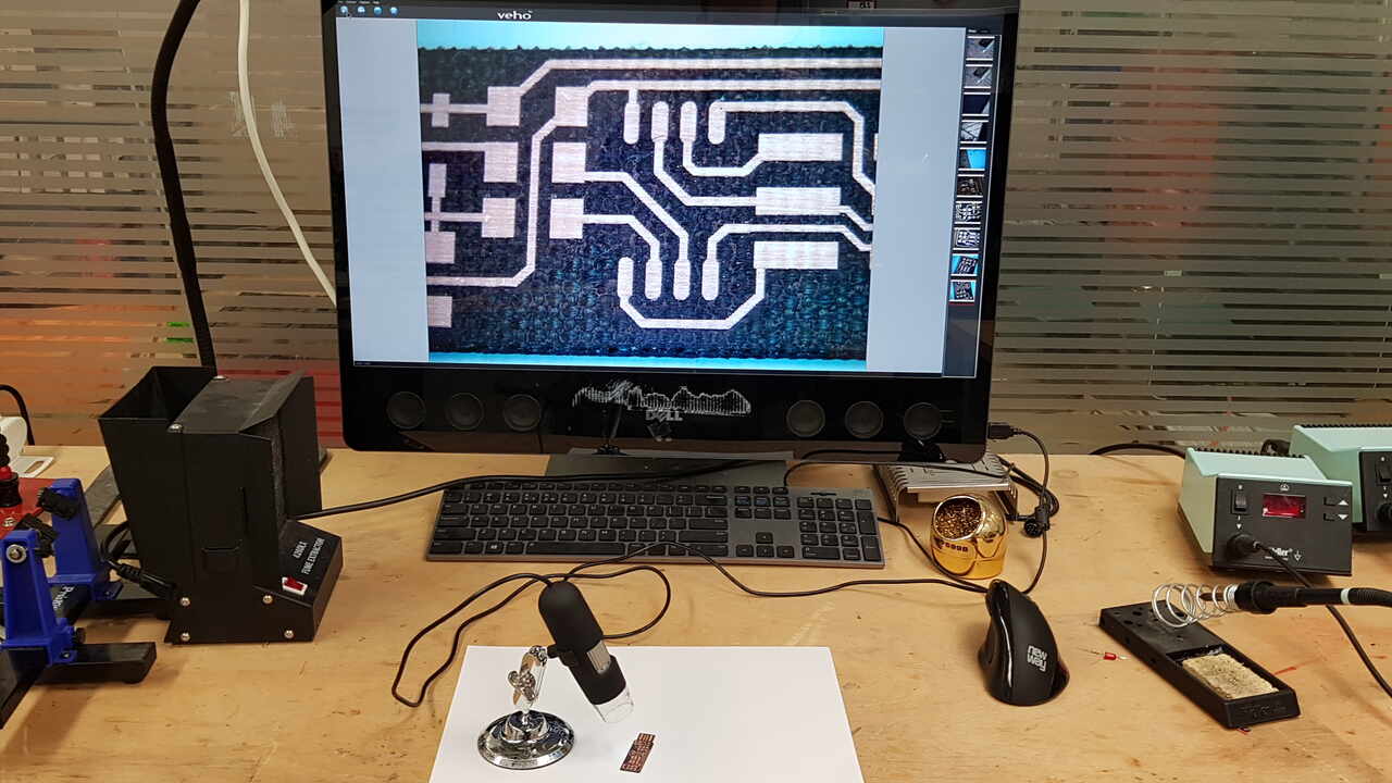
PCB visual inspection with electronic microscope
8 - Peformed continuity tests and made sure that there was no short(s) on the PCB using a multimeter and the electronic microscope. This step is of paramount importance as it can save a lot of time in the troubleshooting that may follow in the steps to come.
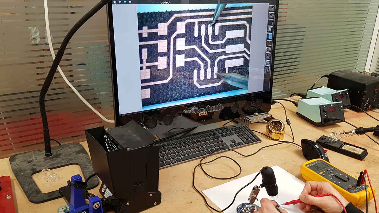
Performing continuity tests with multimeter and electronic microscope
Soldering
First thing to do was to gather all the electronic components needed. In order to do so, I refered to the electronic diagram provided in the tutorial and already presented earlier in this page.
Note : Using a sheet of paper with double-sided tape on it was much appreciated for listing and gathering all the components. This clearly streamlined the soldering process and permitted to avoid confusion between components.
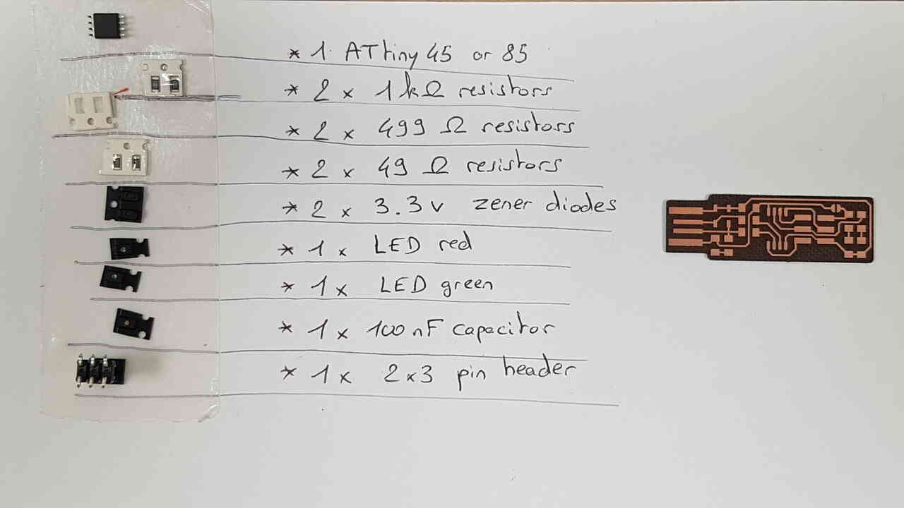
Electronics components list
Here below is presented the soldering station available at fablab Digiscope.
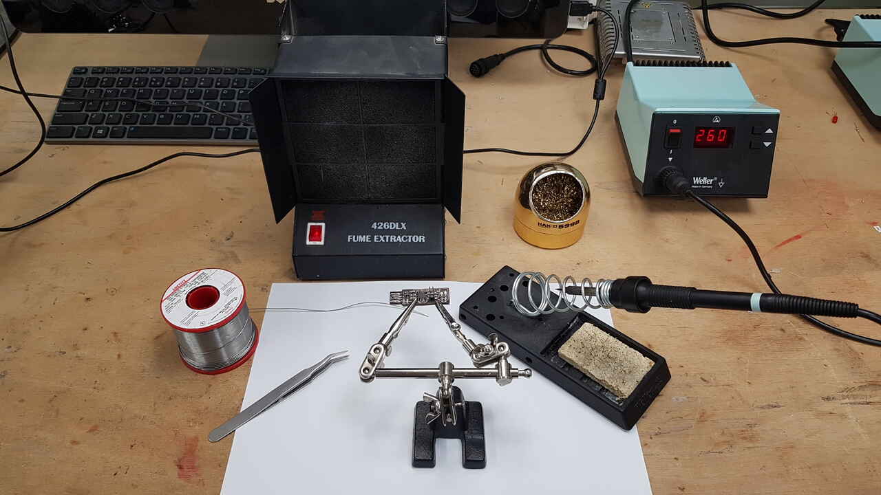
Soldering station
One can notice the presence of the most important elements for soldering :
- soldering iron.
- solder wire.
- fume extractor.
- third hand.
- brass wool (to clean the soldering iron tip).
- tweezers.
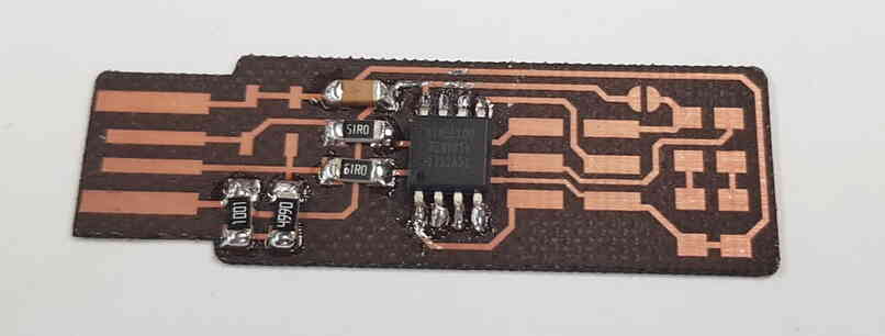
It is generally recommended to solder in the following order : lowest components first, and going from the center of the PCB to the outside. The main goal is of course to prevent some components from impeding the soldering of others. Indeed, it is really appreciated to be able to move hands around the component we want to solder to find a correct position for making the best soldering possible. For the FabTinyISP PCB I have started by soldering first the microcontroller, then the components around it, and to finish the header because even though it is in the center it is also the biggest component in the circuit.
PCB soldering ongoing
And now, some pictures of the PCB fully soldered :
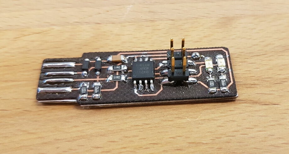
PCB with all components soldered
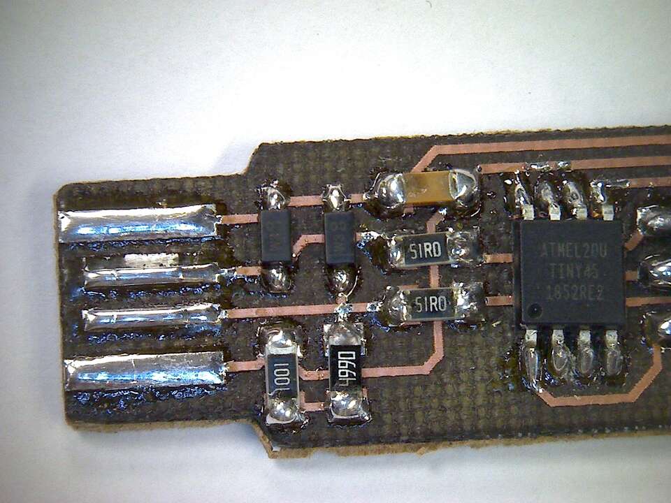 |
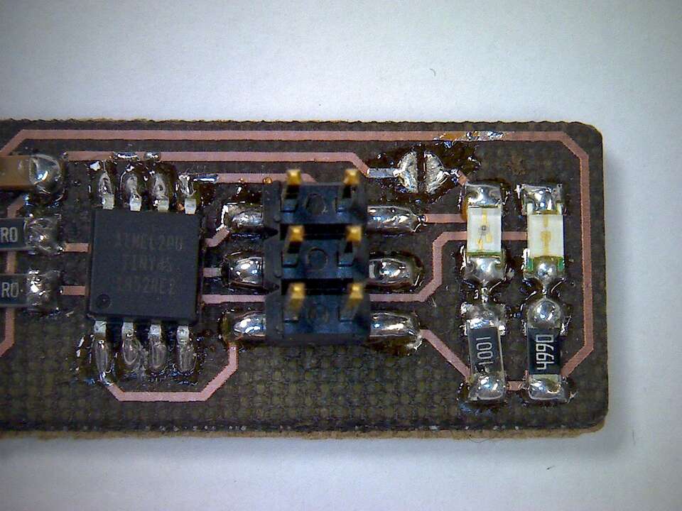 |
| Solders inspection with electronic microscope - Left | Solders inspection with electronic microscope - Right |
It was a first experience for me soldering that tiny components, and my solders are far from being perfect but I feel that I have acquired skills and confidance for the next electronic circuits I will make during the program.
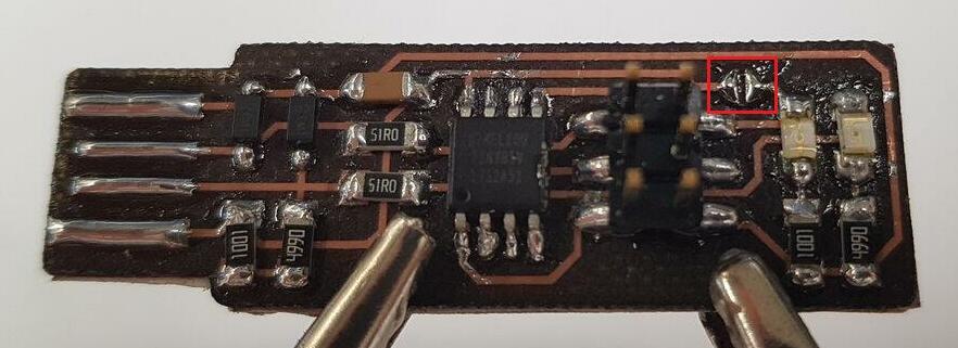
Before going any further with my PCB, I performed a visual inspection of the solders with an electronic microscope AND also performed continuity tests with a multimeter in search for possible shorts. Although I did not notice any particular issue neither during the visual inspection nor during the continuity tests, there was still a short in my circuit that I detected after I encountered issues for flashing the ATtiny85 microcontroller. Indeed, I observed the strange behaviour that both my red and green LEDs were turned ON when connecting the PCB to my laptop via USB. As the green LED was not supposed to turn ON in such situation I have conducted additional investigations with the multimeter in continuity mode and detected a short hidden below the green LED. After I fixed it, the flashing process went fine.
Conclusion : The continuity tests and search for shorts are of paramount importance once the soldering process is done.
Software installation and FabTinyISP final configuration
1- Before I could program a firmware on my microcontroller, I had to setup my computer environment. And to be honest, I was really happy this day that I chose to work on Linux environment as the configuration setup was way easier compare to what it is in Windows environment. Indeed, I only had to run the following command line :
sudo apt install avrdude gcc-avr avr-libc make
2- After I collected the firmware source code from the tutorial documentation, I was able to generate the .hex file to be programmed on my ATtiny85 microcontroller, by running the simple command :
make
3- Then I connected the Atmel Ice programmer to the ISP header of my PCB (respecting the correct orientation of the connectors), modified the configuration file “Makefile” on my computer to indicate the programmer that I was using (“atmelice_isp”), and could flash the microcontroller :
make flash
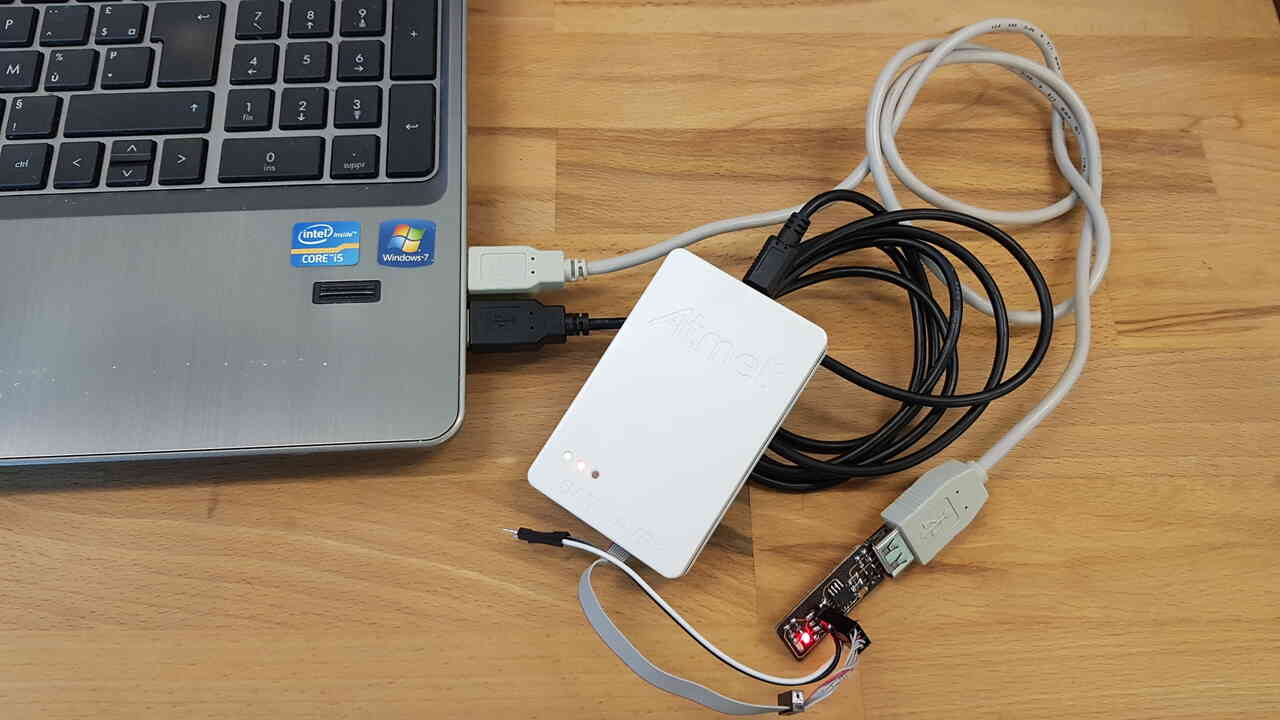
Programming the board with an Atmel Ice programmer
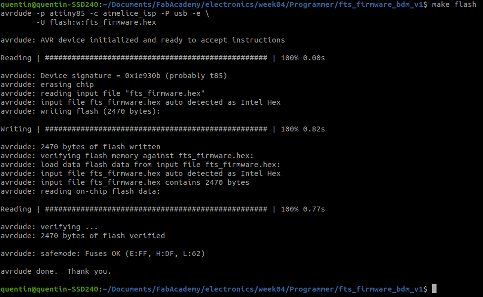
Programming FabTinyISP with Atmel Ice programmer
4- Set the correct fuses configuration to adjust the microcontroller clock source :
make fuses
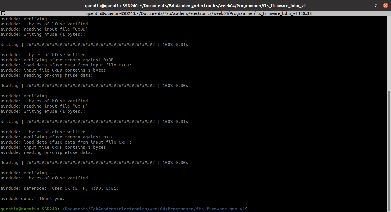
Setting correct fuses configuration
5- Tested that my FabTinyISP was correctly recognized as a USB device by my computer :
lsusb
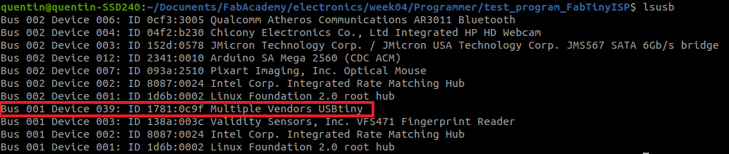
FabTinyISP as USB device
6- Set the fuses configuration so that the RESET pin of the microcontroller is definitely turned into a regular GPIO (General Purpose Input/Output) pin :
make rstdisbl

Changing RESET pin into regular GPIO
7- Removed the bridge on the solder jumper to disconnect Vcc from the Vprog of the ISP header so that the board is now recognized as a programmer and not as a programmee.
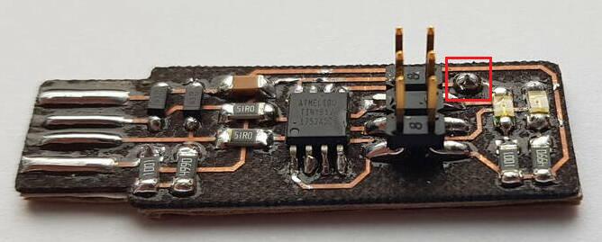 |
 |
| FabTinyISP - solder jumper connected | FabTinyISP - solder jumper disconnected |
FabTinyISP testing
As a final test to make sure that my FabTinyISP could program a microcontroller, I used it to flash on a Arduino Mega board a simple program generated by my colleague Jonah Marss (that I thank by the way!) to make the integrated LED of the Arduino board blink.
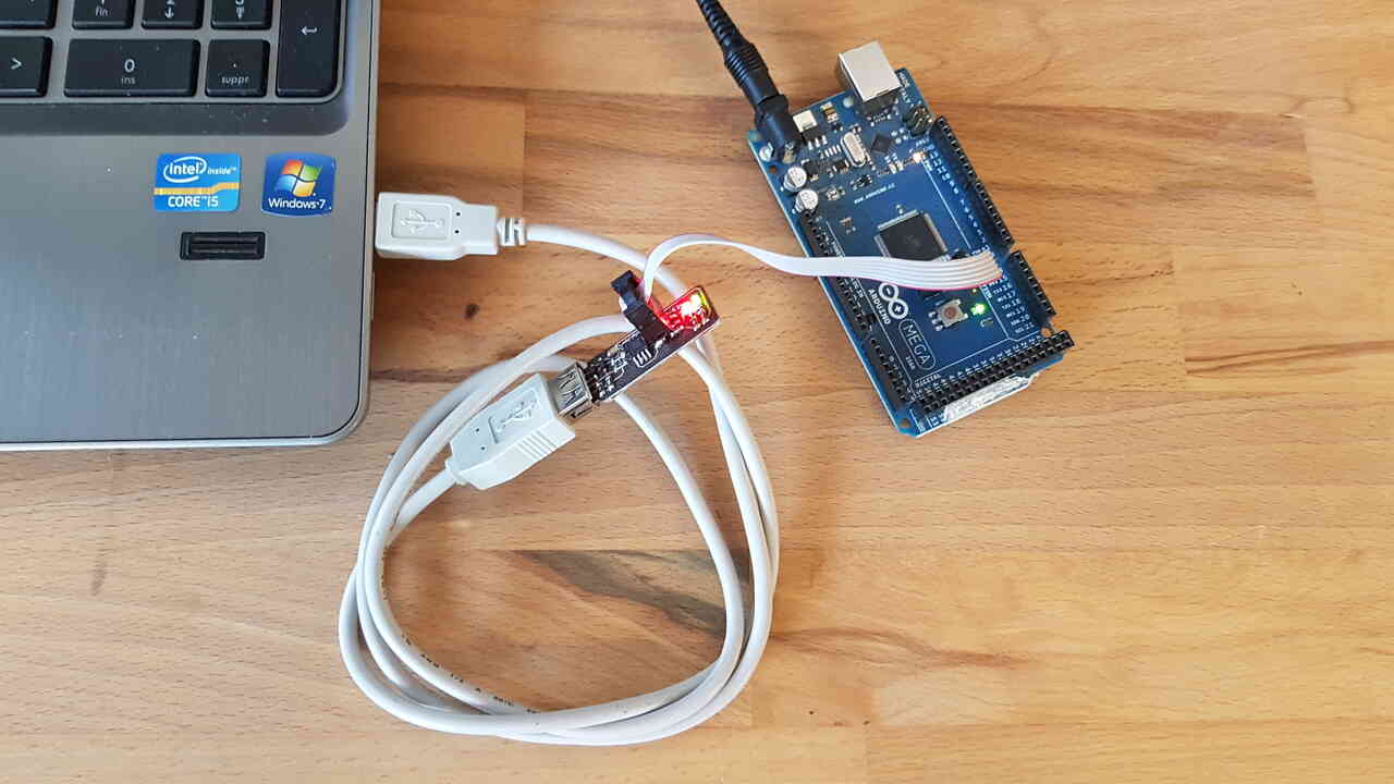
Programming Arduino Mega with FabTinyISP - Setup
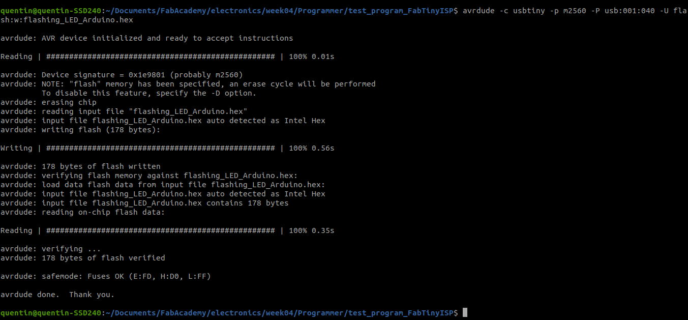
Programming Arduino Mega with FabTinyISP - Command Line
In the command line to flash the Arduino Uno microcontroller here is a brief description of the parameters I used along with the “avrdude” function (be careful that parameters are case sensitive) :
- -c usbtiny => Indicates which programmer is being used (in this case the usbtiny that I just built).
- -p m2560 => Mandatory option that indicates which microcontroller is being programmed (m2560 = ATmega2560).
- -P usb:001:040 => Gives the computer port to which the programmer is connected to (I could find this information by running the “lsusb” command; Note: this number changes each time the programmer is disconnected and reconnected).
- -U flash:w:flashing_LED_Arduino.hex => Specifies what operation has to be performed on the microcontroller memory; in this case flashing a specified program.
Further information on the “avrdude” command can be found here.
As for the program that has been flashed into the Arduino Mega, here below is a screenshot of the C code source (left side) and its conversion into an executable program .hex (right side).
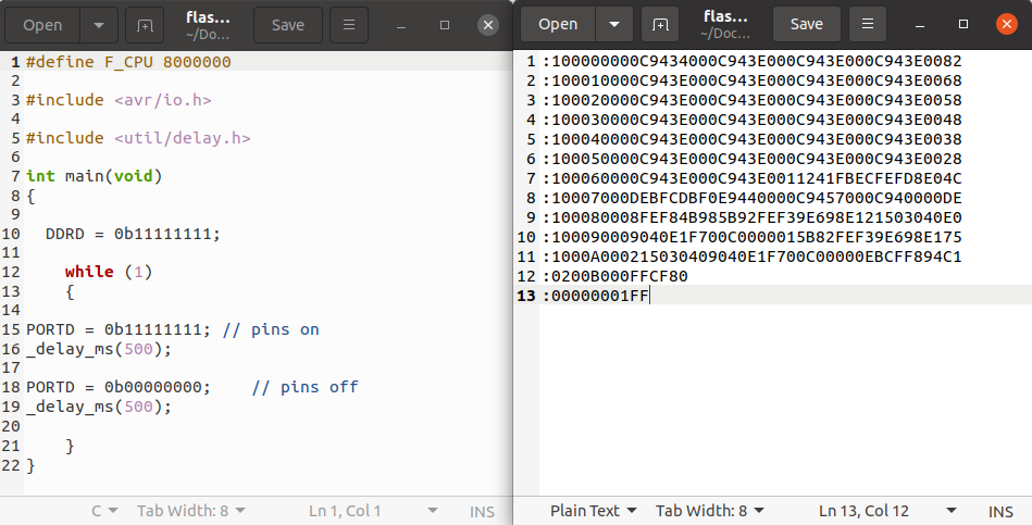
Test program flashed on Arduino Mega - C code (left), “.hex” conversion (right)
Source files available for download here : C code / hex file
Result was successful, which ended well this electronic production week.
Characterization of the PCB production
As a group exercice, we laser cutted a PCB characterization plate to determine what is the minimum space between circuit tracks we can obtain with our Epilog Fusion M2 32 machine.
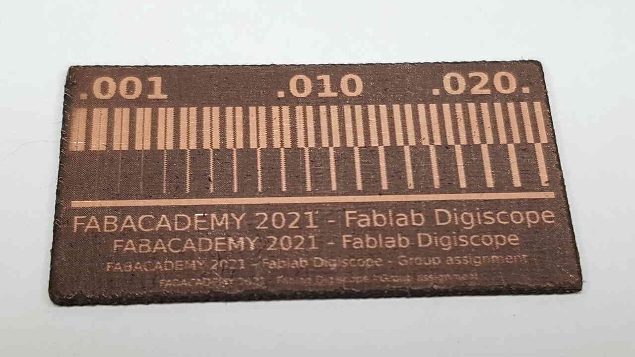 |
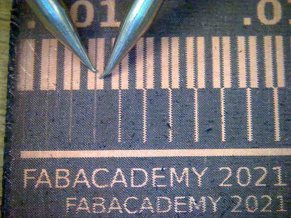 |
| PCB laser cutted characterization plate | Continuity tests using electronic microscope |
Unfortunately it seems that we had an issue with the focus of our fiber laser because copper layer has not been fully removed, making it impossible for us to measure the precision we can get with the machine. We did not find the time yet to rebuild the characterization plate but this is something that we will try to do in the near future.
Source files
The source files of the work presented in this week assignment are available for download here :
- PCB : Traces.png / Cutout.png
- Flashing LED program : C Code / hex file