WEEK 6: Electronics design
This week's assignment was about electronics design
For the group assignment, we had to test the equipment in our lab to observe the operation of a microcontroller circuit board.
The individual assignment was to redraw an echo hello-world board using the software we wanted, and then to add at least a button and a LED. For extra credit we could simulate its operation.
Group assignment:
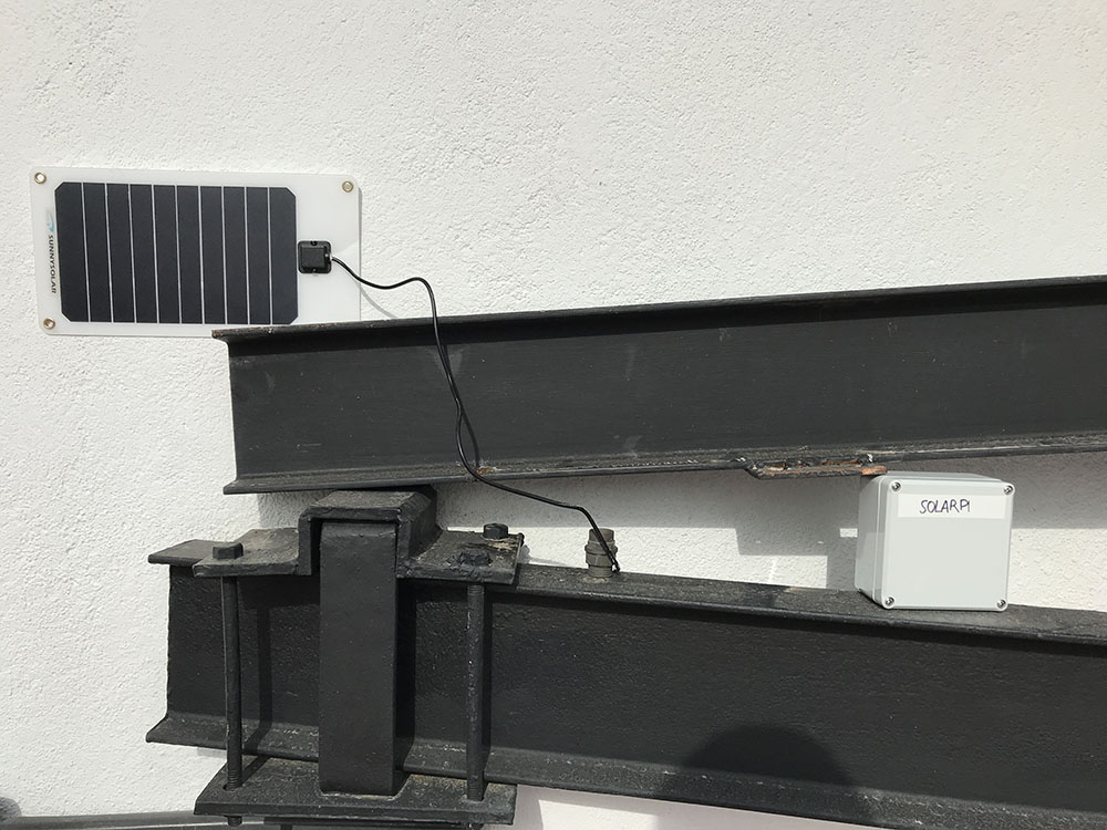
Since last monday, we were working in the lab in a parallel project consisting on setting up a solar powered website. In order to do so, we are using a Raspberry Pi 0 with a solar panel, a battery and a solar power manager.
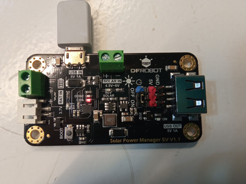
At some point, the solar manager board stopped working, and we saw it as an opportunity to test some measuring equipment we have in our lab.
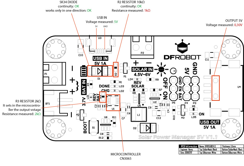
The "SOLARPI":
The power manager:
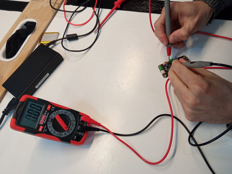
Testing with the multimeter:
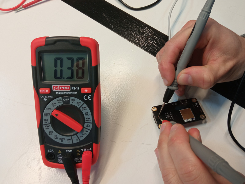
We had an output voltage of 0,38V, when we should have 5V
These are the tests and measures we did in the board:
Sheme of the CN3065 microcontroller:
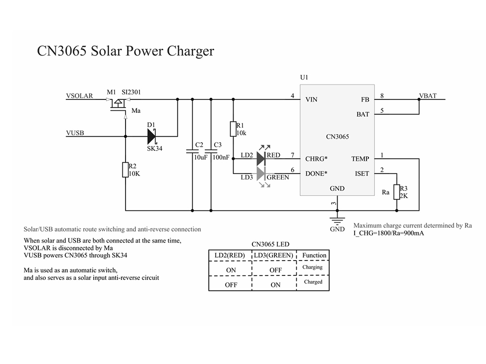
After measuring all the components around the microcontroller, and having conected the board with an usb cable providing 5V, we concluded that it might be a problem either with the microcontroller, or with the resistor R2, because this one is giving a 1kΩ resistance when it says 10kΩ in the scheme.
Individual assignment
For the individual assignment, I decided to start redesigning from scratch a board provided in the fabacademy documentation. I chose the ATTiny 1614 thanks to a recomendation of my local professors.
I used KiCad with the libraries of our lab
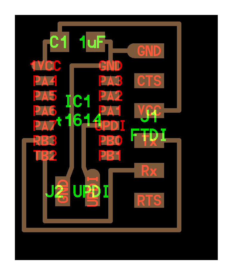
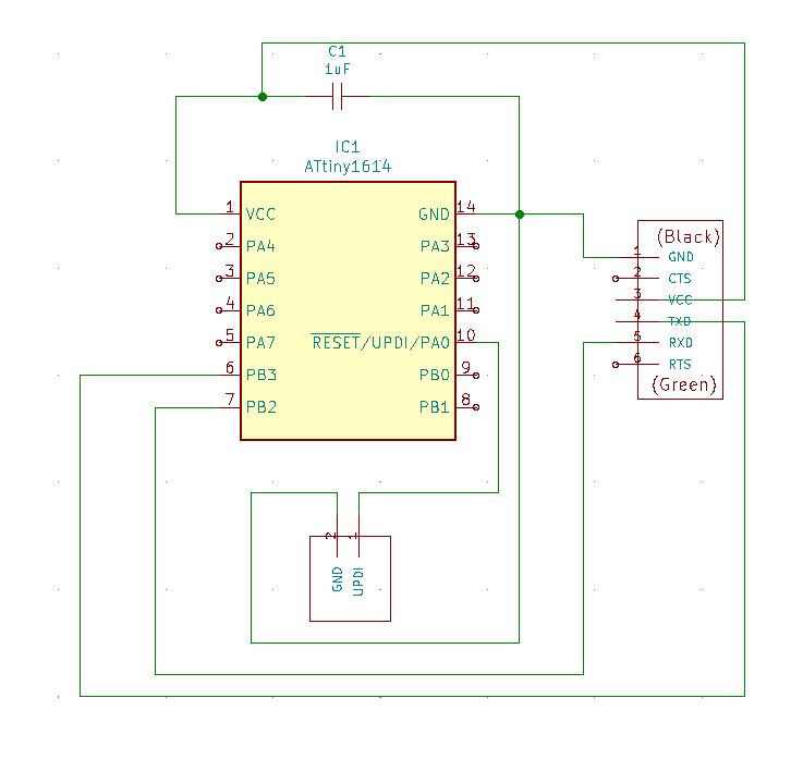
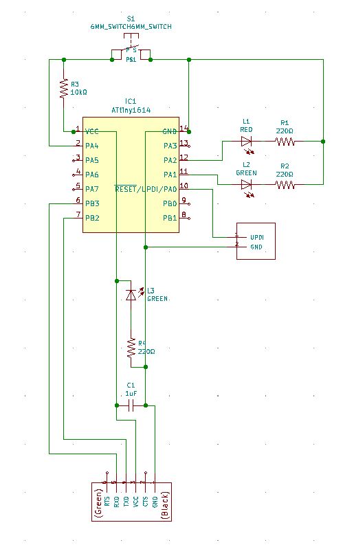
Redesigned schematic layout:
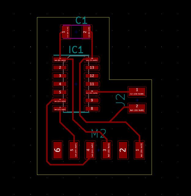
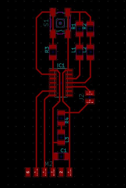
Redesigned PCB layout:
Then for the assignment itself, I added a switch, a power LED, and a couple of leds more with their appropriate resistors.
For the schematic design, the power LED is connected just after the FTDI connector, going from GND to a 220Ohm resistor, and then to the LED that goes to VCC. It's important here to take into account the direction of the LED.
The other two LEDs, are connected to the digital pins PA1 and PA2 and then to GND through a 220Ohm resistor, so that the LEDs will turn on in case the pin is High.
The switch is connected to the PA4 pin with a pull-up resistor, so that the pin will be allways high unless we press the button and close the circuit to ground.
The procedure I followed in KiCad was the following:
- First I went to Shematic Layout Editor
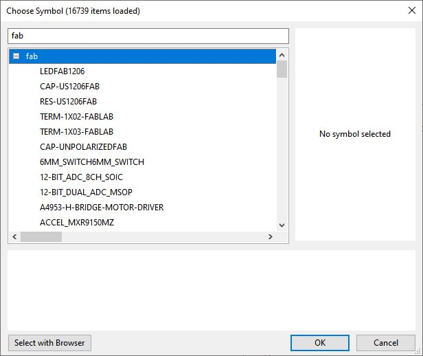
- Once there, we can start placing symbols from:

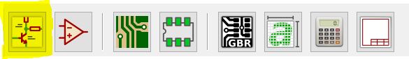
- Then we choose the symbols from the library and place it in the canvas
- Once we have the symbols, we have to connect them with wires

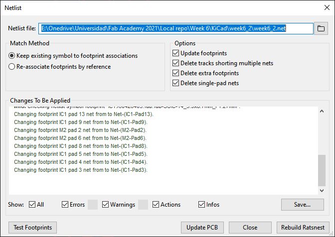
- After we have the schematic layout finished, we have to generate the netlist

- And save it in the folder we want
- Then we can go to PCB layout editor
- And from here we can load the netlist we saved
- Choosing the folder where it's saved
- Then we should see all the component in the canvas. We just need to organize them in the desired position.
- Once we have all the components placed, we can connect them with tracks. We can edit the width of them by right clicking or by going to pre-defined sizes.
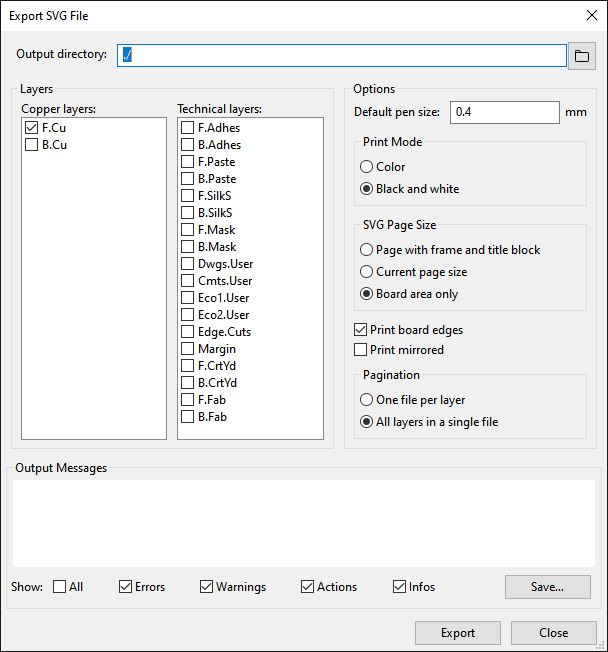
- The last step is to export the svg layout of the traces and the footprints. We can do that from File > export > svg.
The schematic layout:
For the PCB design, I tried to make it as clean and simple as possible.
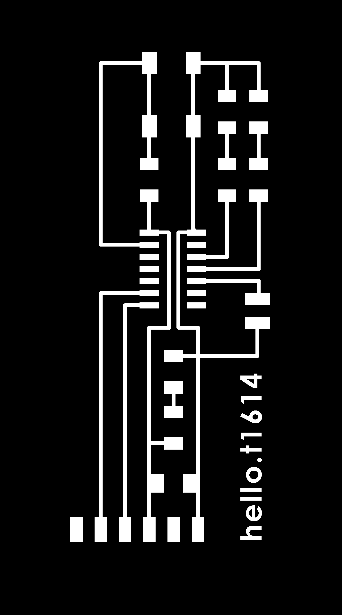
Then, I redraw it a bit in Illustrator in order to align some traces and fix some corners. I exported the two files (traces and outcut) to PNG format at 1000dpi.
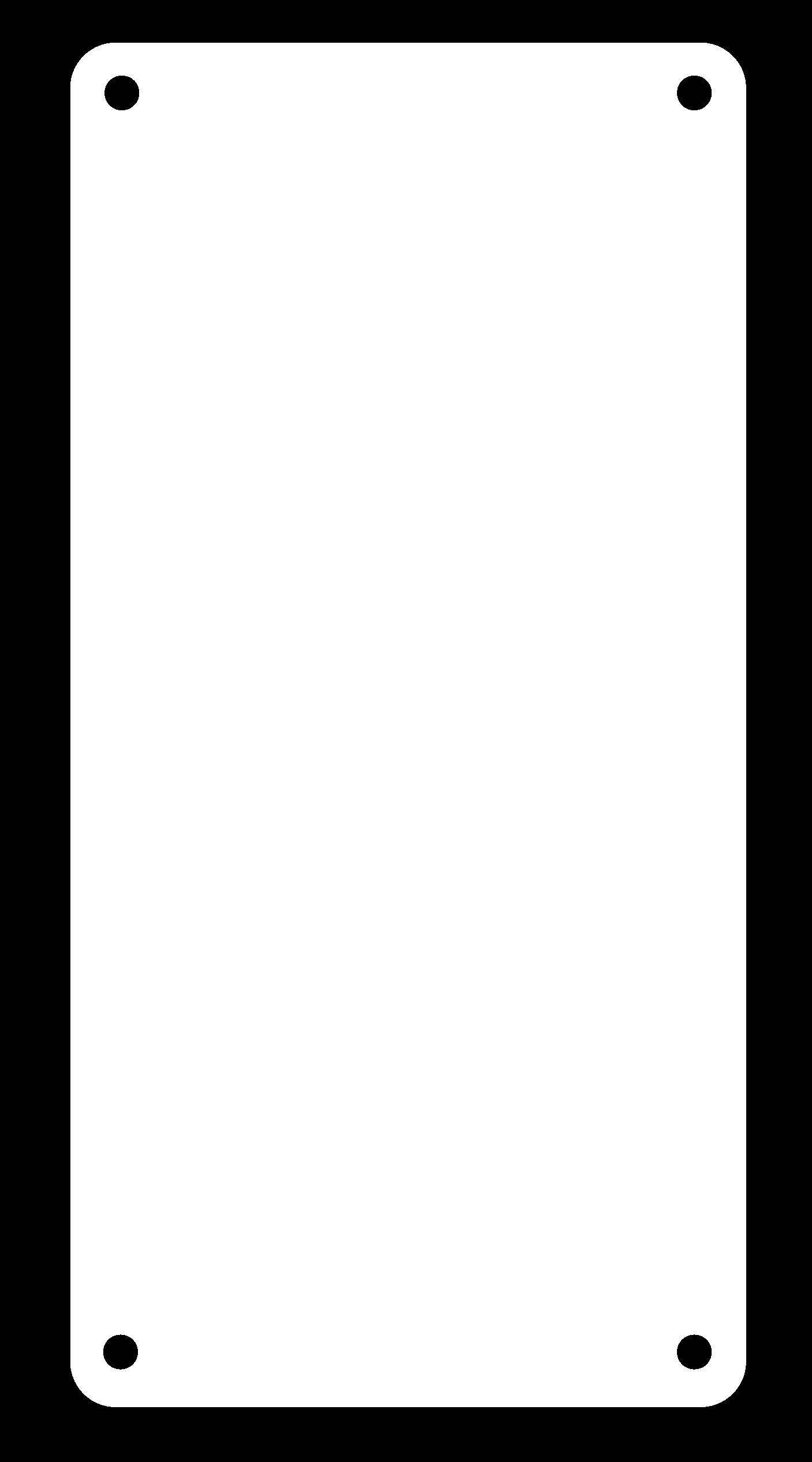
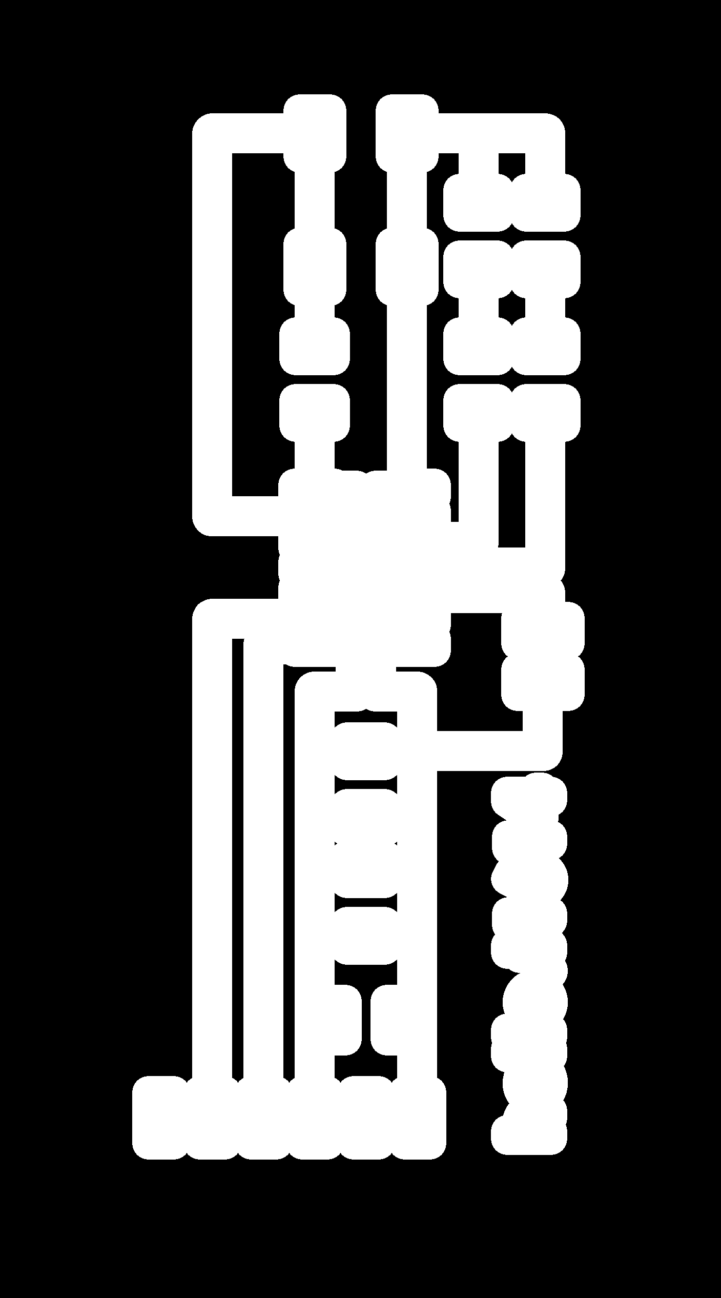
The outcut:
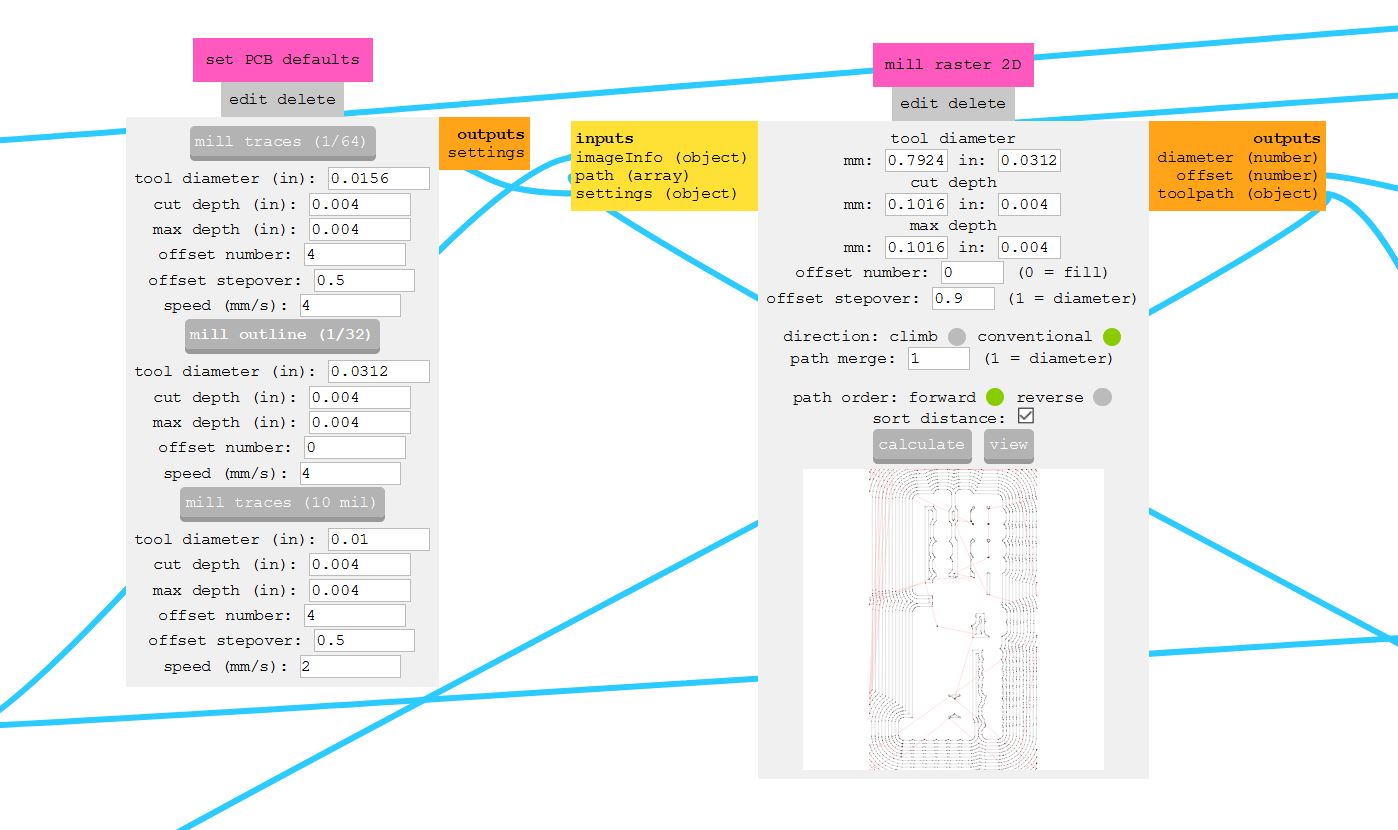
In order to make it even cleaner and simpler, I decided to mill all the board and take all the copper out.
To do so, I thought that it would be faster if I could do it with the 1/32 endmill. I struggled in the beginning, but then I found that when we generate the file in modsproject to mill the traces with the 1/64 endmill, we are able to download a png with the resulting board after milling the traces. So I took this png and I uploaded it again to modsproject. You need to be careful here, and ensure that the dpi is the same as the other pngs, because it is taken as 72 dpi when I was working with 1.000 dpi. Then I adjusted the 1/32 endmill with the depth of the 1/64, and I adjusted the offset number to 0 in order to make a fill. I also adjusted the offset stepover to 0.8 in order to go even faster.
In this way, I milled the board in 3 steps:
- Traces with the 1/64
- All the rest of the copper with the 1/32
- Outcut with the 1/32
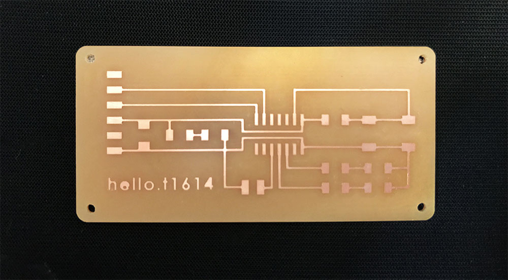
The result was a really clean board:
Then I soldered all the components in place, checking the schematic design, and testing the LEDs with the multimeter in order to solder them in the appropriate direction
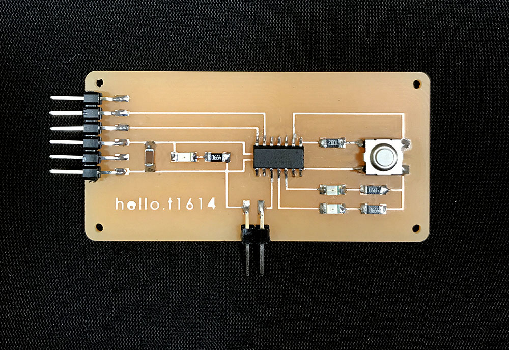
Lastly, I tried to program the board to make the two leds blink. I followed both the Adrian Torres website from last year and this example about programing ATtiny microcontrollers with Arduino IDE.
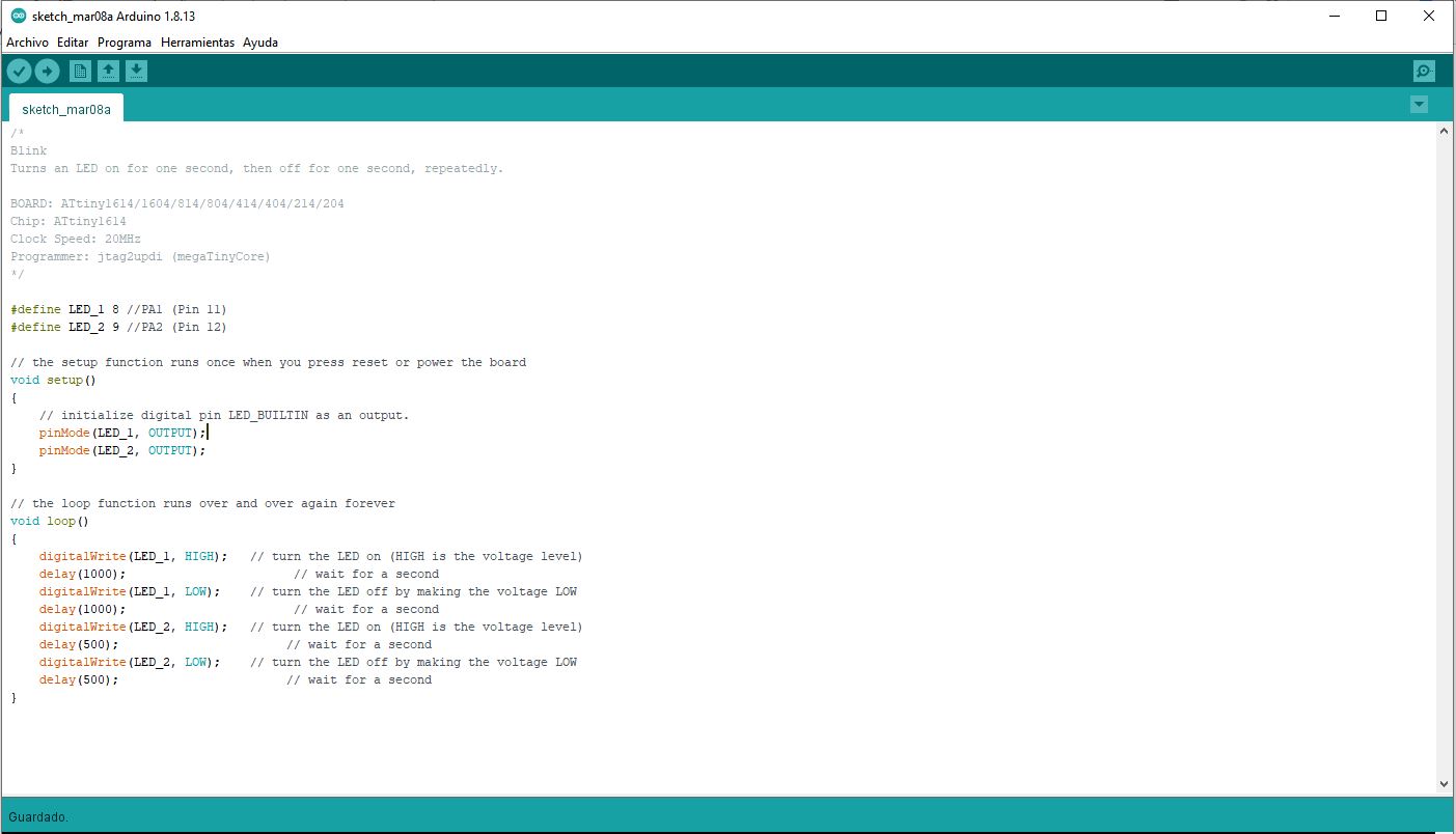
I connected the board using the UPDI and FTDI boards I made two weeks ago. To provide power I used a FTDI cable we have in the lab because my UPDI has no power pin.
So the sequence of the connection was: Computer > USB cable > FTDI board > UPDI board > ATTiny board
I used Arduino IDE, where I had to install the libaries for the ATTiny 1614 as is explained in the embeded programming week.
Then I just loaded the basic blink example where I had to define the pins of the LEDs. Lastly I compiled it and then uploaded to the microcontroller. It's important, before that, to check if the proper port is selected, for example by disconnecting and connecting it again.
In the end, I was able to make the two LED blink at different speeds, a very satisfiying feeling considering it was the first time I programmed anything I made.