Assessment
-
Group assignment
Use the test equipment in your lab to observe the operation of a microcontroller circuit board (in minimum, check operating voltage on the board with multimeter or voltmeter and use oscilloscope to check noise of operating voltage and interpret a data signal)
- document your work (in a group or individually)
Individual assignments
Learning Outcomes
Have you:
linked to the group assignment page
Documented what you have learned in electronics design
Explained problems and how you fixed them, if you make a board and it doesn't work; fix the board (with jumper wires etc) until it does work.
Included original design files (Eagle, KiCad, - whatever)
Included a ‘hero shot’ of your board
Loaded a program and tested if your board works
-
Home
Draw me Like one of Your French Circuits
I am a big fan of Fusion 360, so I decided to work with Eagle for this excercize since they are both Autodesk Products. I have done some work in Eagle a couple of years ago, but I was surprised at how much it has changed
and how much easier it has become to use since then. I opened up the software and we were instructed to download the schematic and an Eagle library from Alex's page.
In Eagle, libraries contain part names and the shape of the package. These parts correspond to parts available by manufacturers, and their footprint is made available in order to include them into our designs.
The Fab library file we downloaded contains a selection of components and packages that are stocked at ZOI. By sticking to these we can be sure that we won't have compatibility issues when trying to populate our boards.
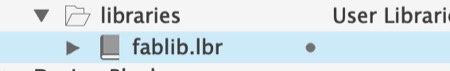
At this point we had to add the fab library to our EAGLE library. This is a simple procedure. When Eagle was installed on my Macbook, it automatically created an Eagle folder in the documents folder on my computer.
We simply placed the Fab library file into the lbr folder and it was ready to use in Eagle.

In the library menu on the Eagle homepage we also have the option ef enabling and disabling libraries by clicking on the green or grey circle next to the library name. I find that there are generally far too many
libraries activated at one time, and this makes it somewhat hard for me to find parts for my designs. For this reason, I like to deactivate most of the libraries and only activate the ones that contain the parts that I know I'm going to have to use.
In this case I knew almost all of my parts were going to come from my Fab library, so I deactivated every other library. I later found that I needed a header from the Molex connector library, so I went back and activated it when I needed it.
This process helps me to avoid clutter and simplifies my workflow.

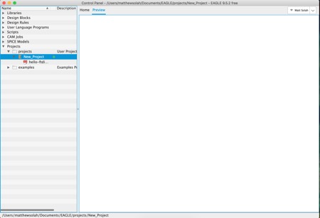
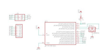
Now that I had my libraries in order, I could move on to working on the schematic. Luckily there were many examples of Echo boards provided for us. We decided to work on the Attiny44 example. I created a project in Eagle and added my schematic to it.
I opened up the schematic file and the basic circuit was laid out.
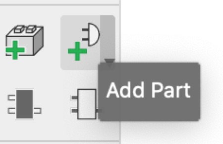
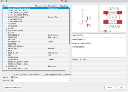
To complete the assignment I had to add some components to this circuit. In order to add parts I had to select add parts in the left menu and find the parts I was looking for in the library. Once selected I was take back to my schematic page, and
I could place the selected component in the drawing. Once placed I can place more identical copies of the component, or I can press ESC on my keyboard to return to the part selection menu. From here I could either select another part to add to my circuit
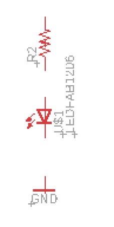
or press ESC again to exit the part selection menu. I placed an LED and a few resistors, along with a 4 pin header to accomodate my the temperature and humidity sensor that I plan to add to my circuit in order to use for my final project.

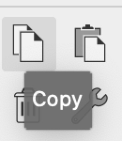
I was also going to need some ground and VCC attatchment points. In order to ensure that Eagle ties all of my VCC and GND points to each other, I decided to use the copy tool rather than add them as new components. Selecting the copy tool will duplicate
whichever component is selected, allowing you to add an exact copy of it to your cicuit.
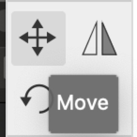
Once the parts were added to the schematic, I could move them and place them where I needed them on my drawing.
This is done using the move tool. Selecting the tool and left clicking your component will allow you to move it around, and right clicking while the component is selected will rotate it 90 degrees. I placed the components where they were needed.
I am including images of the LED portion of the circuit in order to illustrate.
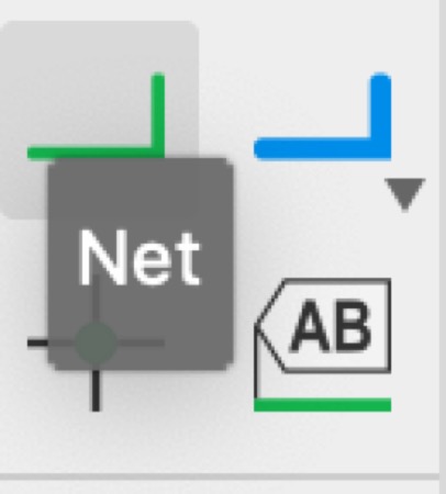
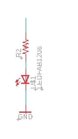
I had placed my parts in position, and now I had to connect them together. The Net tool allows you to draw "wires" between components, and this tells the program that those components are connected at specific points. This will tie into the board
layout portion and ensure that traces are generated at the correct places.
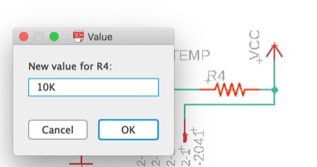
At this point I wanted to name my components and give them the appropriate values. Defining all of this is necesarry in the schematic in order to allow you to look at the schematic and determine exactly which components were used, and the part names and
values are included in the BOM in order to help prepare the components for soldering when it is time to populate the board. This is done by selecting the Name and Value tools in the menu, and typing in the name or value once a component is selected.
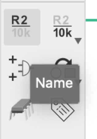


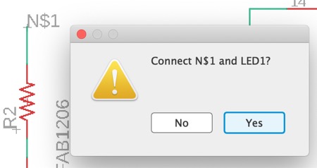
In many circuits containing IC's such as the Attiny44 the schematic can quickly become confusing due to the large number of connections to the IC pins. In order to clean up the design we can use Labels.
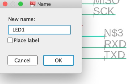
A label allows us to place a name on the end of a wire, and then connects any wires that end in the same name.
I used this to connect one of the Input/Output pins of my IC to my LED without having to run a wire across my schematic. This is done by right clicking on the end of a wire and selecting the Label option.
This will bring up a dialogue box that allows you to input a name. Once the name is added to the first side of the connection, the program will give you a warning when you try to label any other
connection to attach them together. The program will ask if you are sure that you want to connect both wires, once accepted the connection will behave in the same way as if it was connected by
drawing a wire from one point to the other.
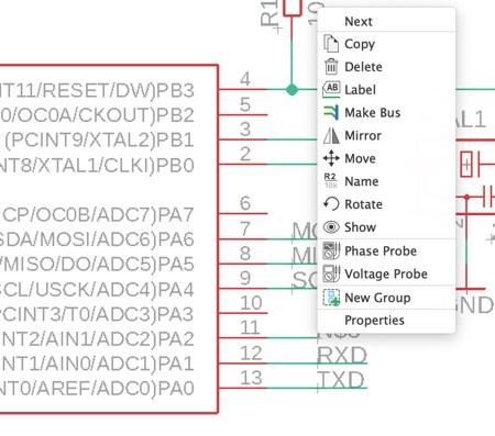
If you make any mistakes, wires and extra components can be deleted with the Delete tool.

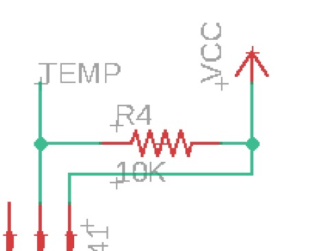
I am going to use a button to trigger an output. In this case it will trigger the LED I drew earlier. I will program the microcontroller to expect a value of 0 (0 volts or ground) in order to trigger the LED.
I can achieve this by tying one end of my button to an input pin on the attiny44 and the other end of the button to ground. This would work, but there is a risk that the voltage at the pin would float between
ground and VCC, and this could cause false triggers to be read by my program. In order to ensure that the pin is always at +5V when the button is not being depressed I used a 10K pullup resistor tied from one end to the same input as
the button and from the other to VCC. My DHT 22 temperature sensor also outputs a Low signal which must be detected by my micrcontroller, so I added a pullup resistor to that pin as well.
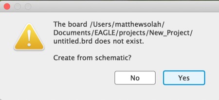
At this point my circuit was ready to begin laying out the PCB design. So far I had not created a board from this schematic, so when I clicked on the Switch to Board option in the top menu I got a dialogue box
with a warning. I clicked through and I was presented with an empty board and all of my components layed out to the left of it.


The move tool allows you to move, place and rotate components like in the schematic.
When designing circuit boards it is very important to account for the manufacturing process that will be used to fabricate them. In this case I will be milling my board the same way I did during electronics production week.
During our tests we determined that the thinnest line we can mill reliably is 0.2mm wide. This also applies for spacing between features. This value will inform the way in which we place our components, and the width of traces we can use to connect our
parts. I tried to make all of my traces 0.4mm wide, but I sometimes had to dip down a bit in order to get some traces between the solder pads of some components.
When placing components on the board I like to keep my schematic at hand in order to be able to plan my component placement. Luckily Eagle makes this easy. By clicking on the same option used to generate the board you can easily switch between your sckematic
and your board for quick references. Another great feature is that the board file is linked to the schematic, so changes in the schematic will be immediately reflected on the board.
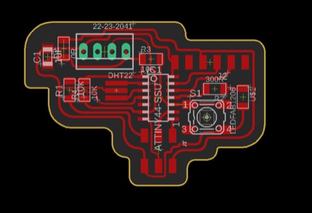
I like to start by placing my main IC first, since I know that many of my components must connect to it, and I find it useful to make it a central feature on my board.
I try to look at my schematic and plan my layout by placing the components that have most connections to the board first. I also tend to place the components and immediately route the traces connecting to it.
I find that the yellow Airwires are harder to understand visually than the traces and they clutter up my visual space, so the quicker I can eliminate them the better. I also try to place related components at the same time.
For example, when placing my LED I place the LED and the 300 ohm current limiting resistor at the same time. By routing components step by step in this way I find that I avoid creating a clutter on my board, I also find that I
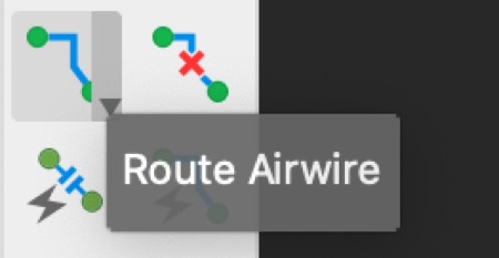
make less errors than I would placing all the components at once. The following image shows my board in a halfway state. I have placed most of my components and routed their connections by selecting the route tool. I prefer to use
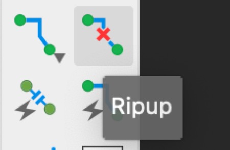
curved traces because I find them more intuitive to route. If errors are made while routing, using the Ripup tool will remove unwanted traces.
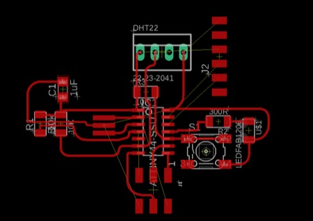
I started off leaving more space than necessary between my componets. This allows me to work more comfortably while trying to find the routes for my traces. Once I have connected all of my components I can
optimize the board by moving the components closer together.
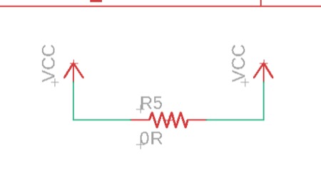
It is ideal not to have to add any jumper wires or 0 ohm resistors to the board, but sometimes there is just no way to avoid it. If I had more time or was more attatched to not having any jumpers, I may have started from scratch and
rerouted the board, however this time I did not want to. The following was my situation, I had a connection to make between some components and my VCC and GND lines, but I couldn´t find a way to do it without having to cross my traces.

In order to be able to cross over my GND trace I went back to my schematic and added a resistor. I connected both ends to VCC and set the resistor value to 0. This added a new resistor component to my board layout, and i could then
connect each end of it to a VCC trace and jump over my GND line, allowing me to finish my layout.

At this point all my connections were made, and I began to move my components and traces closer together. This step optimizes space, and I wanted to try to get my board smaller than it was.
I used the move tool and in most cases I had to ripup the traces connected to each component and reroute them in their optimized location.
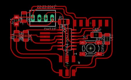

I wanted to shape the outline of my board to follow the contours of my traces, so I made sure to select the Dimension layer from the layer menu and I used the line tool to draw the outline.

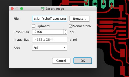
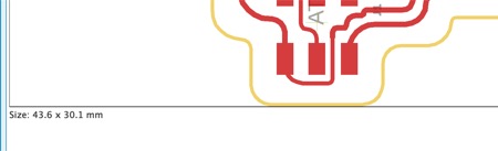
The board layout is now ready to export in a format that will allow its manufacture. In this case I will process a PNG image in Mods for milling in the same process used during electronics production week.
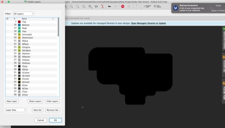
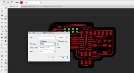
In order to do this I need to export my layout as a high resolution PNG file. If I export it as it is, my image will contain the part names and labels, and this will make it impossible to process the file for milling.
In order to export only my traces and the pads for the connector component, I have to edit my layer settings. This is done by selecting the layer settings option in the top bar, hiding all the layers and then enabling only the layers
that I want to make up the files I will use for milling. I exported two files: One for the traces by enabling the top and pads layers, and one for the outline by enabling just the Dimension layer. It is also necessary to
export the files in monochrome.


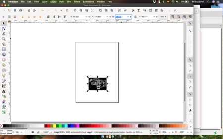
I prepared the file as I did in week 5, but while the autolevel program was executing we realized that the board size was much larger than what I had designed. This was a very confusing error, because
I was sure that I had done everything correctly. I tried re exporting the files, but they were always oversized. In the end, I did a Google search for Eagle scaling errors on Mac computers and found a Forum post that
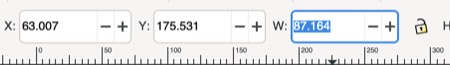
showed that this was an error that has been present on the Mac version of Eagle for some time now. The only solution that worked in the end was to import the files into Inkscape and scale them down by 1/2. This worked and it brought
my file down to the intended size.


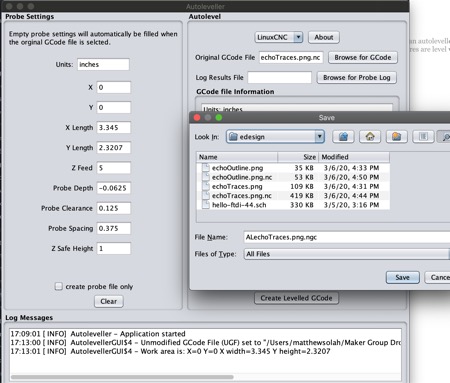
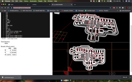
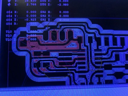
Before milling, I checked my toolpaths on this gcode simulator.
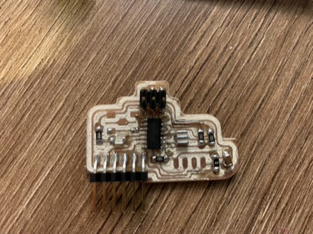
At this point I proceeded to mill my PCB on the CNC router.
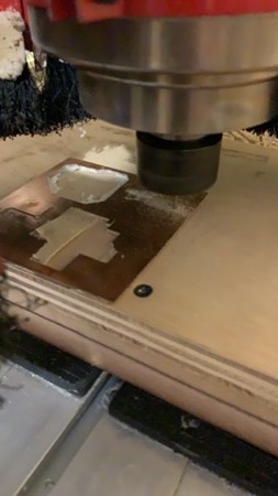
I had been a little bit too ambitious with my routing, and some of my traces were joined. Fortunately this was easily solved by
cutting between them with a knife.
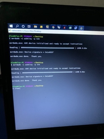
I stuffed my board and we ran a quick test to make sure it was working.