Assessment
-
Group assignment
Individual assignments
Learning Outcomes
Have you:
-
Home
How THIN can you SPIN? Testing Limits to Find Design Rules
In order to be able to design a PCB that can be manufactured easily, it is important to take into account the limitations of the manufacturing process that will be used. These limitations will determine de minimum distance between features, the minimum width, minimum hole and pad sizes, among others. Our design rules are made up of these values, and are generally refferenced by our CAD software in such a way that they will display a warning and/or point out areas in the PCB design that are breaking the rules. (Naughty traces, leave them alone for a second and they go breakin' the design rules just for the sake of it).
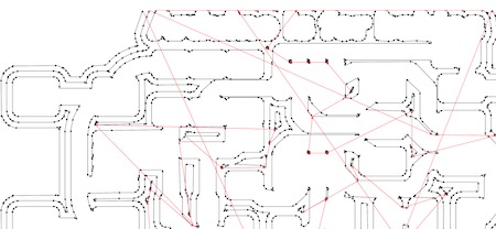
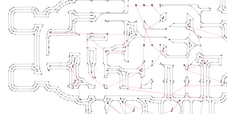
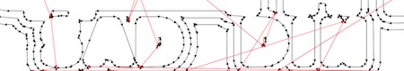
In order to get an idea of the values we should use in our PCB designs, we have been provided with a design to mill.

The idea behind this design is to measure the tolerances we can achieve with our CNC Milling machine. The traces and spaces on this design become thinner from right to left, and it becomes incresingly more challenging for the machine to make without either causing damage to the intended geometry or just blasting it off completely.
In order to prepare this design for milling I used the Mods software located here. This software allows remote access to software processes that allow the user to execute a variety of tasks from a single page by calling each function in a dedicated module. By understanding the way this software processes the image we can arrive at a cursory understanding of our PCB design rules. I started out by opening mods and left clicking to open up my selection menu, and then selecting the following options:

This will display the Mods preset for creating Gcode for PCB milling.
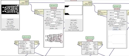
Each of the modules recives an input and modifies it to create an output that can either be exported or handed off to the next module in the chain. The first thing to do is to input a .PNG file, in this case I will input my Line test file. It is important to pay attention to scale. If the information displayed for the measurements in the module is incorrect it is likely that the resulting PCB will not accomodate the components that will be soldered on later.

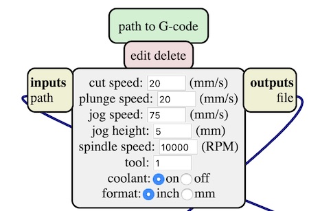
The next module to pay attention to is the one where we will determine many of our milling settings. The following image illustrates this. The Tool Diameter asks us for the diameter of the end mill we will be using to mill this PCB. In this case I used 1/64 inch as my input. The Cut Depth will tell the machine how deep each pass of the cutting tool should be. I set this to 0.4 mm. The max depth corresponds to the final depth of cut. The milling machine will make succeeding cuts determined by the cut depth until it reaches the maximum depth. Shallower cuts make for a cleaner milling process, but more cuts means a longer milling time. Deeper cuts speed up the process, but increase the risk of breaking an end mill or causing damage to your work.

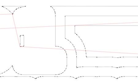
The Offset Number determines how many perimeter offsets the tool will make. In essence, it determines how much of the excess copper will be removed from the copper clad board. The following images illustrate the effects of changing this setting from 0 (fill) to 3. Each line on the image represents a path that will be milled.

The six modules to the right of the window are image processing routines. In order to properly generate milling paths the image must be converted into a vector format. This is what those modules do.
By clicking on the calculate button in our main module we tell the program to run the imported .PNG image through the image processing modules, which return their result to the main window and display the milling paths in it. We can preview our milling path by clicking on the View option.
The next window will determine our speeds and feeds. I used the settings in the following image to mill my line test.
Once all of these settings were in place, I clicked on Calculate in order to generate my GCode file. The original files are included at the bottom of this page. If I were to run the following gcode on the milling machine, I would mill my traces onto the copper clad board, but my PCB would still be attached to the stock material. In order to remove it, I have to generate another cut file that will cut out the outline of the Line test. This file was also provided for us.

All it is is a black outline that shares a common origin with the previous design. It is prepared in a similar way, but changes are made to the maximum depth and offsets settings. Maximum depth is changed to 1.7, which tells the machine to mill through the width of my copper clad board, and offets is set to 1 in order to mill a single path in steps through the material.
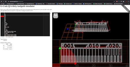
Alex shared a gcode simulator that can be found here. by copying the gcode into this window we can take a look at the preview it generates in order to make sure that the milling machine will be travelling the way we want it to. Any lines shooting off into spae would be a bad sign.
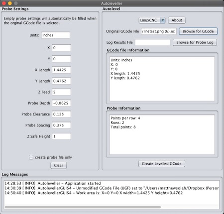
Finally, we were provided with an autoleveller. The function of this program is to run the milling machine through a routine in order to generate ofsets in the gcode that ensure that the milling procedures are level with the material to be milled. The autoleveler adds code to the beginning of the gcode which contains the autolevelling routine.

Milling Vanilling
Once I generated my Gcode files I was ready to send them to the milling machine and run my cuts. We began with a safety overview.
The first rule of CNC milling is you don't talk about CNC milling. Wait, wrong movie.
End mills are sharp. Don't touch the pointy bit. It will cut you and you might cry in front of everybody. Also, blood will oxidize your copper traces. Don't bleed on your PCB.
End mills are fragile, especially the crazy thin ones used for PCB milling. Also End mills are expensive. Also, special end mills like these take a long time to get to Ecuador. Don't drop them. Handle them with care, or your instructor might cry in front of everybody.
Our CNC machine is a big beast of a thing. Stay out of its way. It has more horsepower than you care to get in the way of. It will break your leg with less effort than it takes you to bend a bendy straw. Know where your hands are and don't stick them near any moving parts. Especially don't stick your fingers near the furious spinny thing that's pushing 10,00o RPM. You will probably cry in front of everybody if you do that.
We all want to look stylish while we prototype, but the CNC mill won't judge you for your looks. The furious spinny thing, also known as the spindle, loves to suck in any dangly pieves of clothing. Don't wear a scarf, keep you sleeves short or rolled up and leave your Superman cape at home.
10,000 RPM is very fast, and any end mill that breaks could become a sharp flying projectile. Eyeballs are soft, squishy things. Tungsten Carbide is the exact opposite of soft and squishy. Your eyeball will lose a fight against a flying end mill shard. Wear safety glasses.

The standard end mills used to mill PCBs are 1/32 inch, 1/64 inch and 0.010 thousandths of an inch in diameter. Our Fab Lab has these in stock for when they are required. However, it takes a long time and a big shipping fee to get those into Ecuador. For this reason we used 30 degree and 45 degree V tip mills in order to mill or line test. The results from these fall within the range required to successfully mill PCBs.
The first step is to attach the material to the work table. We did this using double sided tape. The next step is to place the milling tool into the collet. It's important to hold the V bit in place with a finger. This will prevent the bit from either falling onto the work surface and damaging your work or the bit. Once the chuck is tightened far enough the bit should be secure enough not to fall out.
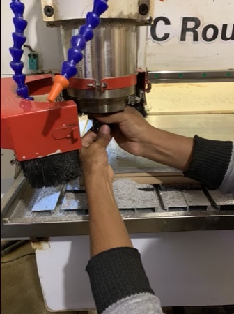
The collet must be tightened further in order to hold the bit securely while the machine is working. In our machine this requires the use of two wrenches, one to hold the spindle in place and the other to rotate the chuck. For safety, the v bits come fitter with a removable rubber sock that is kept in place until the bit is installed, this covers the sharp tip and prevents accidental cuts, as well as protecting the tip from impact in case of a fall. We used a 45 degree v bit to mill the traces on our line test.
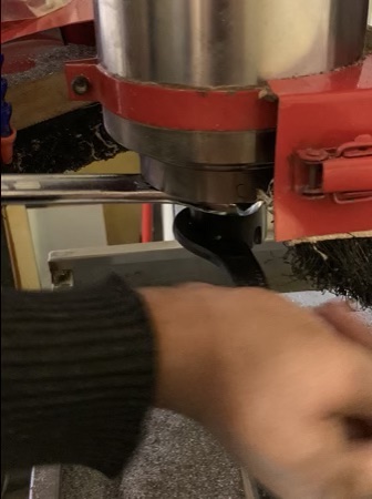
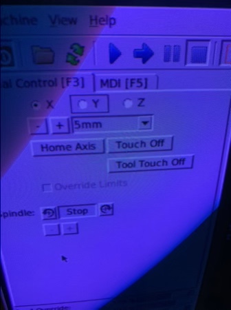
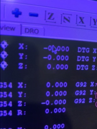
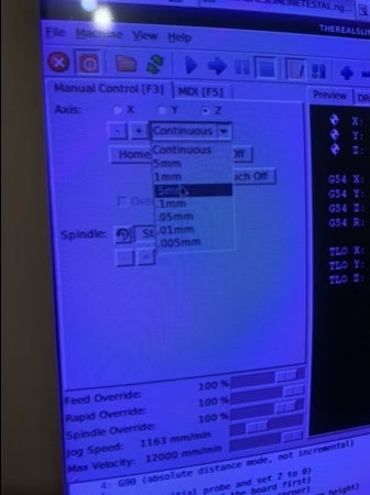
Once everything is set we can define our origin. The origin will be the point that is considered to be the starting point for each axis while the machine is cutting. It is important to take the placement of the origin into consideration in order to ensure that the cut will take place on the material that you place in the machine. In this case the origin was set to the bottom left corner of my material in the XY axis, and within 3 mm of my material in the Z Axis. In order to move the toolhead into place in the X, Y and Z axes we used the jog controls from the CAM software The Autoleveler will ensure that the Z origin is set immediately on the material once it runs.
We loaded the gcode for this file into the cutting software, but I got an error. Our instructor Alex told us that this error happens frequently with the autoleveler, and it is due to some text that is added to the beggining of the gcode by the autoleveler program.
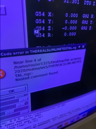

Once this text was erased we saved the gcode file and tried again. The error was gone and we could begin the autoleveling routine. In order to do this in the safest way possible we ran the program step by step rather than running the cut program from start to finish. This gives us more control and it allows us to respond more quickly if we experience an error. We also kept a finger on the P key on our keyboard, this key is used to pause the program if we see something go wrong. The program uses an electronic probe that is held by hand on the material and makes contact with the copper clad board and senses the moment that the tool makes contact with the material. the program takes note of the Z position of the toolhead at this moment and uses it to offset the machine's movements as it works through the cutting movements. The machine will probe the first point 3 times. Once the three probes are finished, we can be sure that the machine won't ram the tool into the material and we can run the rest of the autoleveling program continuously.


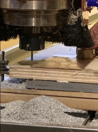
Once the autoleveling is finished, the machine will automatically pause before beginning the job. At this point we continue to tun the program step by step until the spindle starts spinning. It is important to wait until the speed ramps up completely before begining the cut. It is easy to know when it has reached top speed because the frequency of the sound it makes will stop increasing until it remains constant. At this point we can hit the button to begin the job. The machine will start milling the paths until it is finished, and then it will return to its origin and switch the motor off. We jogged the motor away in order to get a better view of the results.
The results looked adequate, but we still had to cut the piece off. The 45 degree v Bit's angle is too shallow, and cutting through the material with it would probably cause it to remove too much material, as its kerf increases with cut depth due to the angle on the curring edge of the V bit. For this reason we switched to a 30 degree V bit before running the final cut job. We can no longer run the autoleveler because all of the probe points are on top of the material we just milled, and since the system requires conductivity between the probe and the tip of the bit, the probe would fail. In this case we have to set our Z origin manually. In order to do this we move out cutting tool to the X Y origin. Once there, we set the spindle to spin. We then jog the toolhead down carefully, being sure to use the appropiate step distance, until it just makes contact with the material. We then set the Z origin in the software.
At this point we raise the toolhead once again and we begin the job by running the program step by step until the spindle begins to ramp up. Once at a constant speed we run the entire cut job.

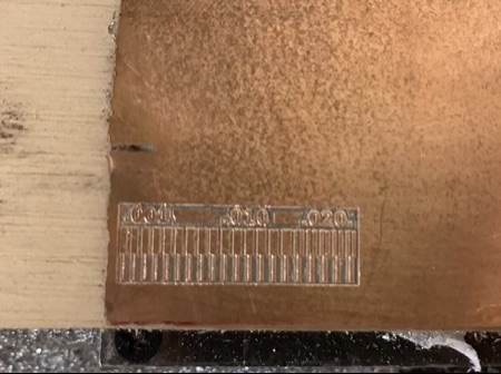
Our cutter managed to make it to the fifth line from rhe right. This means that as long as we keep the spaces between each trace and pad on our boards above at least 0.020 inches we should have no problem making them in our lab.
A Board of my Own
my precious
Now that I had gotten some practice it was time for me to mill my own board. I chose to reproduce Alex's version. I downloaded the traces and outline files from his page and imported the traces into Inkscape.
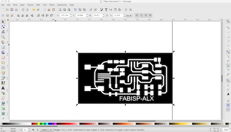
I didn't want to copy his board exactly, but I also didn't want to draw up a schematic and route a board myself in this case. I decided to compromise by expressing the true extent of my feelings about the process of growth and maturity I have gone through so far in Fab Academy.

After attempting to prepare this over and over again in Mods I had to give up on my message because the letters were too small to mill.
This made me sad, so I updated my board to express my angst.

With larger letters, this file could be prepared easily in Mods with a 1/32 inch mill diameter. We found this to be within tolerance for milling in consideration of our design rules determined in the group excercise. I did the same for the outline to cut my board out. I used the same setting as were used in the group excercize.
I used the same procedure used in the group excercize to create the gcode and mill my board on the CNC router. Unfortunately I was in a hurry while milling the PCB, so I did not get any photos of the milling process, but I have a Photo of the half-stuffed board that shows the results.
As far as the eye could tell there was only one issue with the milling process. I failed to inspect the milling paths with as much detail as I should have,
and I didn't realize that there was not a cut path in between two of the pads where the Mini USB connector would be soldered later on. Fortunately this was
easy to fix by manually cutting a space between the pads with a sharp utility knife. The circled area indicates the spot where the cut was made.
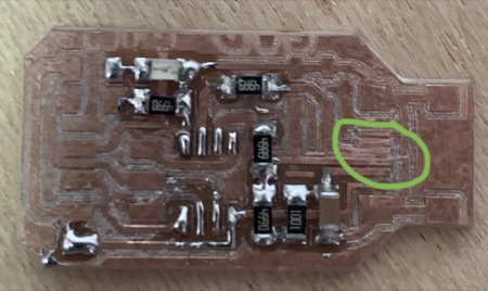
Once the board was milled I proceeded to stuff the PCB using the components provided to me by my lab after submitting my Bill Of Materials (BOM) to my instructors. The components used are the following:
BOM
- 1 x ATtiny45 or ATtiny85
- 2 x 1 kΩ resistors
- 2 x 499Ω resistors
- 2 x 49Ω resistors
- 2 x 3.3v Zener diodes
- 1 x red LED
- 1 x green LED
- 1 x 100nF capacitor
- 1 x pins of 2x3 pins