♦ Electronics Design♦
Highlights of the week
|
|
In this week we are going to make PCB design by using different software like Eagle,Kicad.In wednesday lecture Neil told about various softwares and also he told about test equipment.On next day komal maam gave lecture on pcb desinging and basic about electronics.So I started desinging using Eagle software.In this week I explored different softwares.
Please refer group assignment here:
Group Assignment: use the test equipment in your lab to observe the operation of a microcontroller circuit board.
Individual Assignment: redraw an echo hello-world board,
add (at least) a button and LED (with current-limiting resistor)
check the design rules, make it, and test it
Before started designing I learned about eagle using tutorial.Also I learned Kicad software.But my instructor told me to use eagle software.Apart from this I used fusion 360 for seeing 3D view.
Eagle
Eagle contains a schematic editor, for designing circuit diagrams. Schematics are stored in files with .SCH extension,parts are defined in device libraries with .LBR extension. Parts can be placed on many sheets and connected together through ports.The PCB layout editor stores board files with the extension .BRD. It allows back-annotation to the schematic and auto-routing to automatically connect traces based on the connections defined in the schematic.In eagle we can save file in different format like image,gerber file.Eagle can run on any operating system like Windows,Linux. It is free software or we can download educational licence for 3 years.User interface is easy.
Kicad
Kicad is open source software.We can install it on windows,linux.It facilitates the design of schematics for electronic circuits and their conversion to PCB designs.KiCad uses an integrated environment for all of the stages of the design process: Schematic capture, PCB layout, Gerber file generation/visualization, and library editing.We can also see 3D view in Kicad.By using bitmap2component we can convert images to footprint.
Individual Assignment:
For individual assignment I started with Eagle.I installed Eagle software on my PC.Also I installed Kicad but for designing I go with kicad.As Neil told explore different softwares,so I did that.I started my schematic design in eagle.
Open Eagle,click on new and select schematic,because we need to draw shematic first.
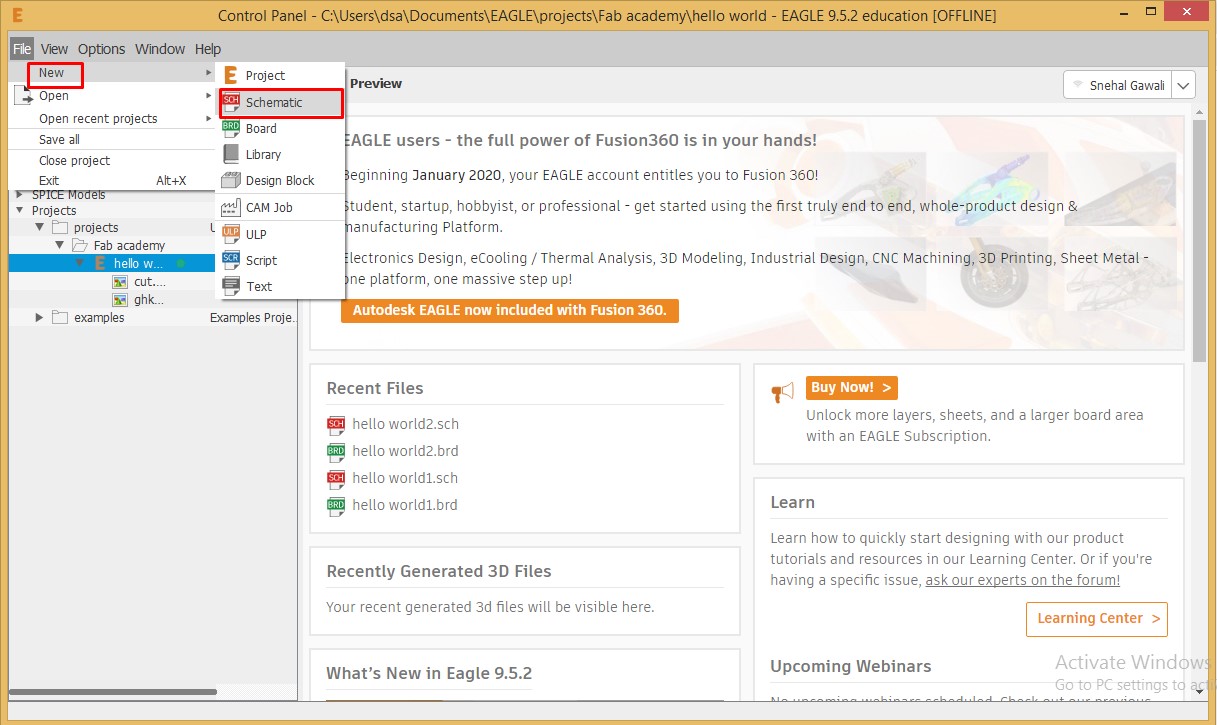
Eagle Window
We have to make echo hello world board,for that we required "fab.lbr" component library.From Neil's documentation download that library.
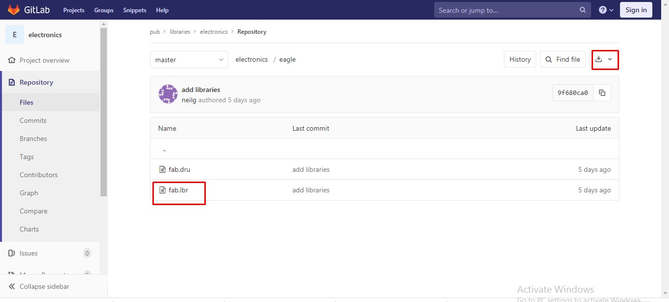
Fab Library
To add library type "use" in command line of schematic section and search the folder in which you downloaded the file and open it.You can see library manager window ,click on available and browse library and click on use.
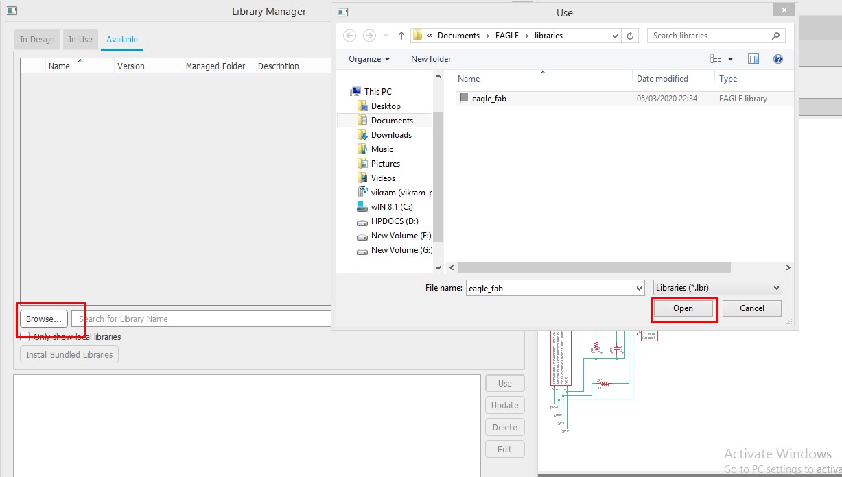
Addition of library
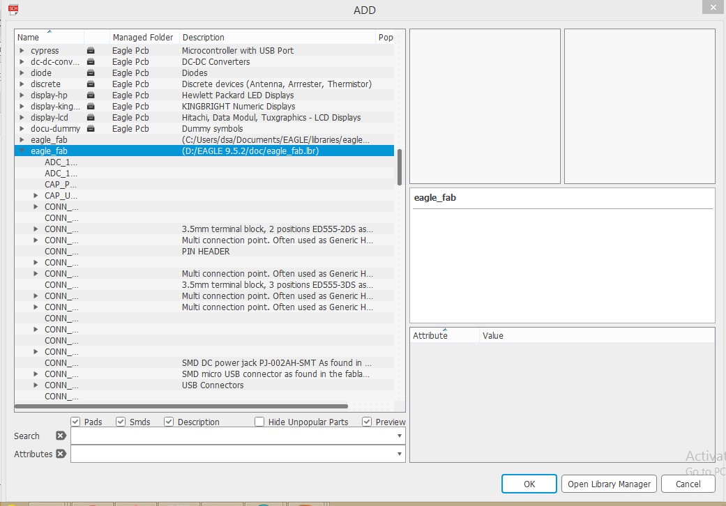
To check whether library is added or not,type "add" in command line .In that we can see "eagle_fab" library.
Check library
To select the components type "add" in command line and select components from fab library.We can see the footprint of component in side window. Neil has given different attiny IC package.Also he provided png image of that.We have to redraw that circuit by adding switch,led and current limiting resistor.In my case I added attiny45,resistor,capacitor,switch,led and pin header.
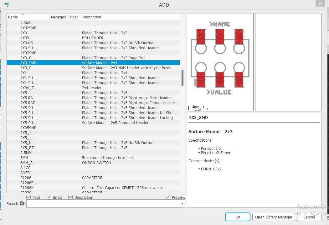
Add component
In schematic window there are many tools like NET,Junction,Move,Value ,Name.Each one have certain role.We will see one by one.
MOVE:To move the component from one place to another we use move command .We have to select component which you want to move.
NET:Net is like wire,If we want to connect two components,we use net command.
JUNCTION:When we connect components ,it shows circle that is called as junction.It shows that two wires are connected.
NAME:Name is also called as lable.If you dont want too much wiring ,so you can use lable.Just you have to give name for that pin where you want to connect.
VALUE:Each components have some value.By using value command we can assign value to them.
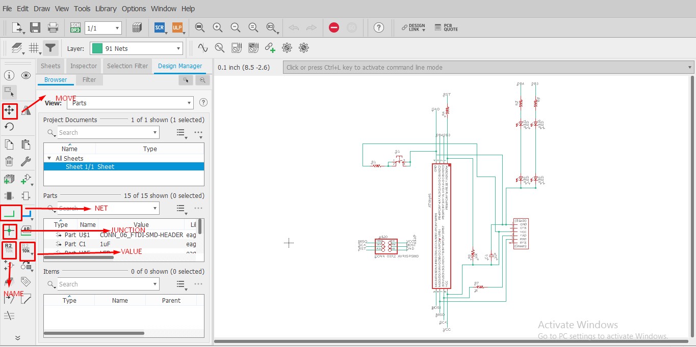
Schematic
After completion of our schematic , we have to check is there any error in our circuit.There are two types of error ERC anf DRC.In schematic we check ERC error i.e. Electrical rule check.Go to tool click on ERC .If you have errors in your circuit it will show that.By clicking on that error you get to know that where is error in your circuit.
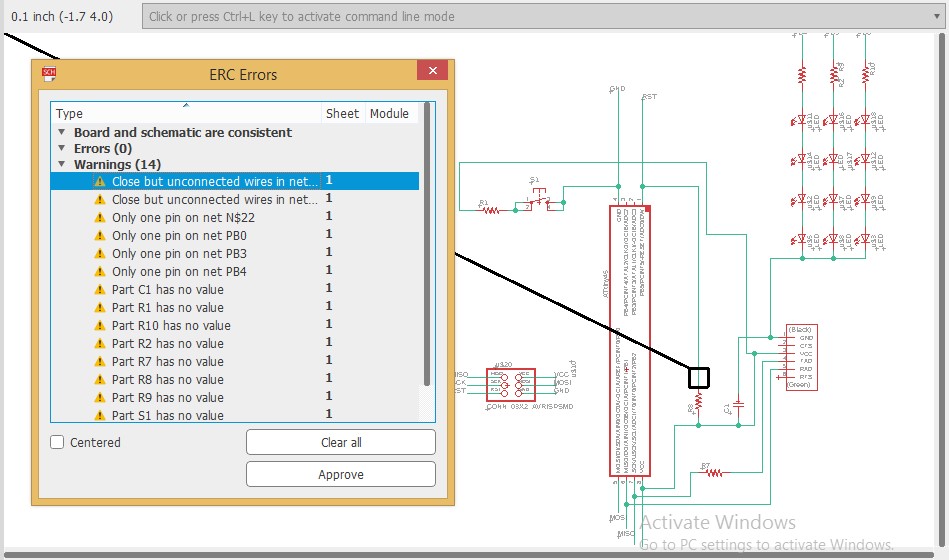
ERC check
Now for pcb ,go to Pcb board.You will get all components there.Now according to our design place the component.We can route in two ways .One by autorouting and other by manual routing.You have to set trace width.
Most important thing is ,we have to set clearance value as per our clearance test.
If we havnt set value trace will get short.So I added clearance of 0.025 .
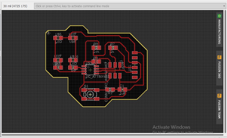
Board Window
As we seen,in schematic there are some tools like that in pcb board there are also some tools
Layer Setting:In layer setting we can set the layers.For trace file we required top layer and for cut file we required dimension layer.So in layer setting we can set layer .
Route: Route means trace path between two components.By using route command we can route pcb manually.
Autorouter:Using this we can autoroute our PCB.
Ripup:Ripup command used for delete the trace.
Text: We can add any text in our pcb.
Shape:Usually we see square or rectangle pcb .If we want something different shape like circle ,polygon.We can use this tool.
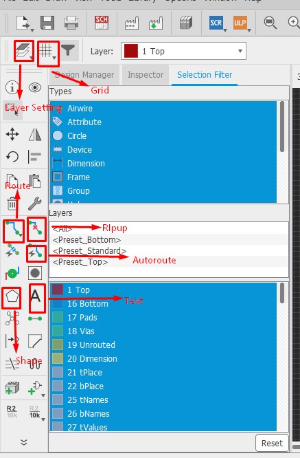
Tools
As we checked ERC error like that we have to check DRC error in pcb board i.e design check rule. Go to tool and click on DRC check and and check it.
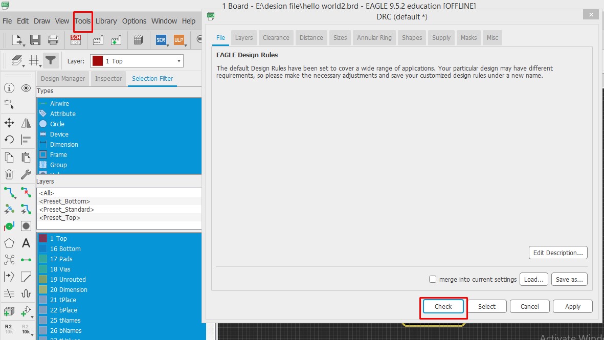
DRC Check
For SRM 20 we require PNG file ,so we need to save file in png format.For that you required two files one is trace file and other is cut file.For trace file we required top layer,bottom layer and pads.
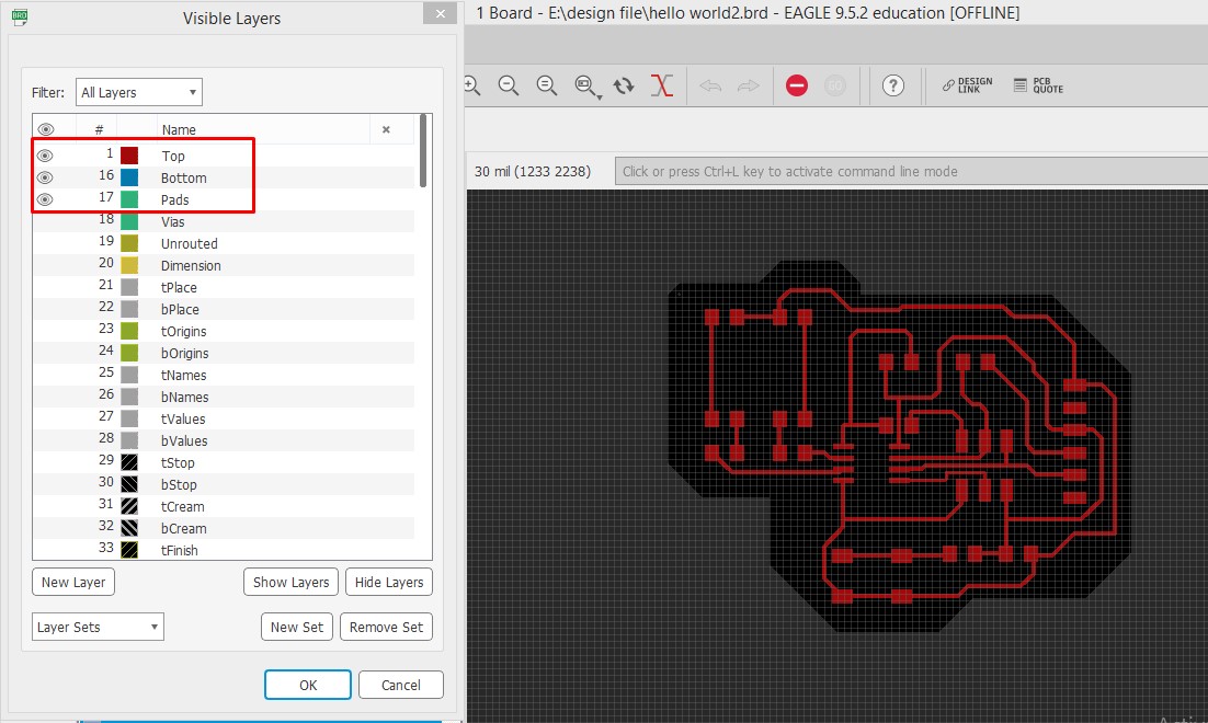
Layer selection
For cut file we required only dimension layer.So select dimension layer only.
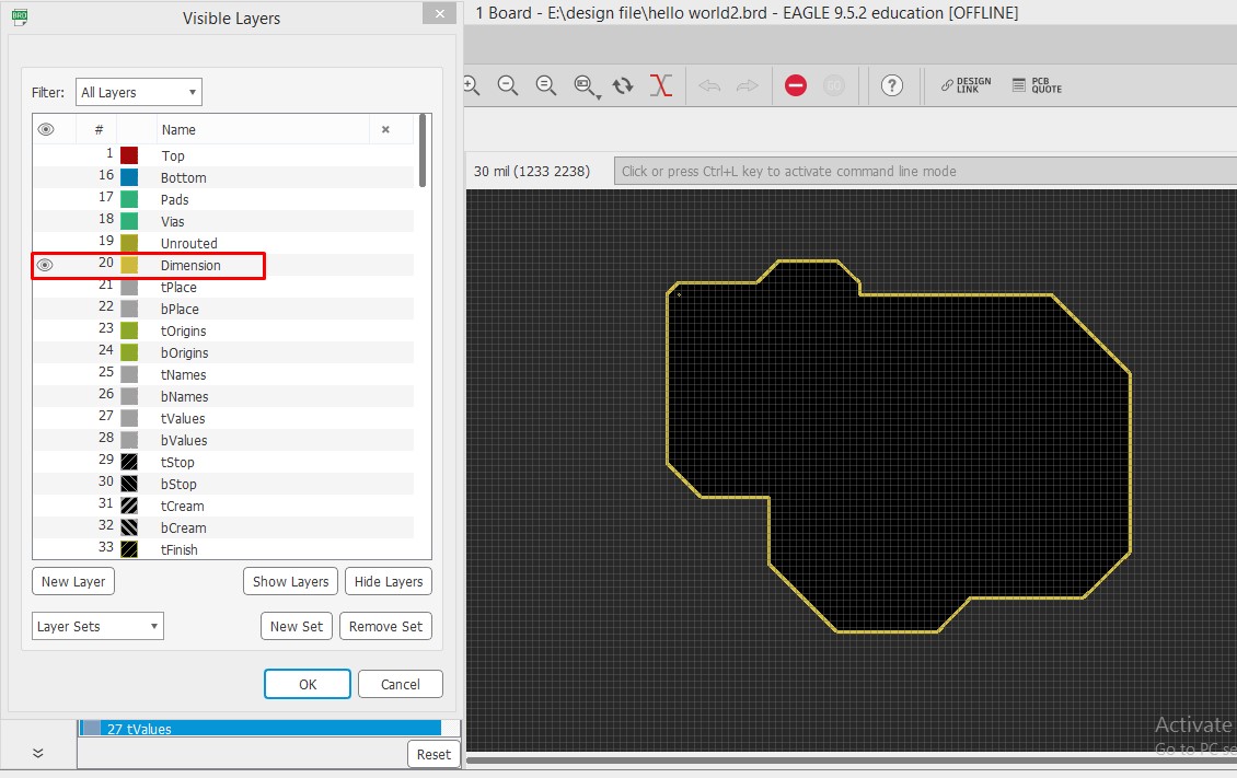
Layer setting
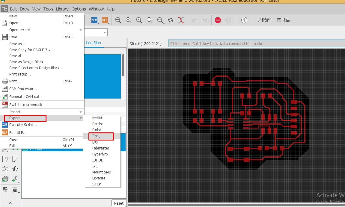
To save file in PNG format,go to file click on export and select image option.
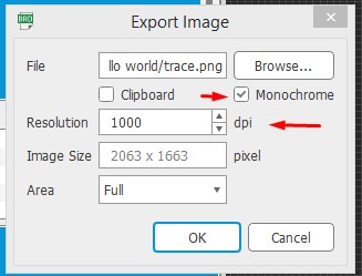
By clicking on image option we can see this window.Click on monochrome.Set resolution as 1000dpi.Click on browse and select location where you want to save file.
Save file
We cant see 3D view in eagle.We required Fusion 360 to see 3D view.So for that I exported Schematic and pcb board file in fusion 360.Go to file click on new electronic design.Add schematic and pcbfile from computer.
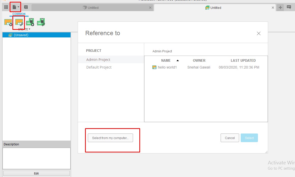
Fusion 360 window
After adding both file we can see screen like below.Now can see your 3D view.
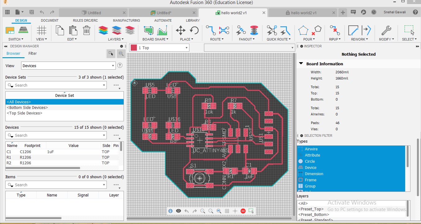
add file
This is the 3D view of final PCB.
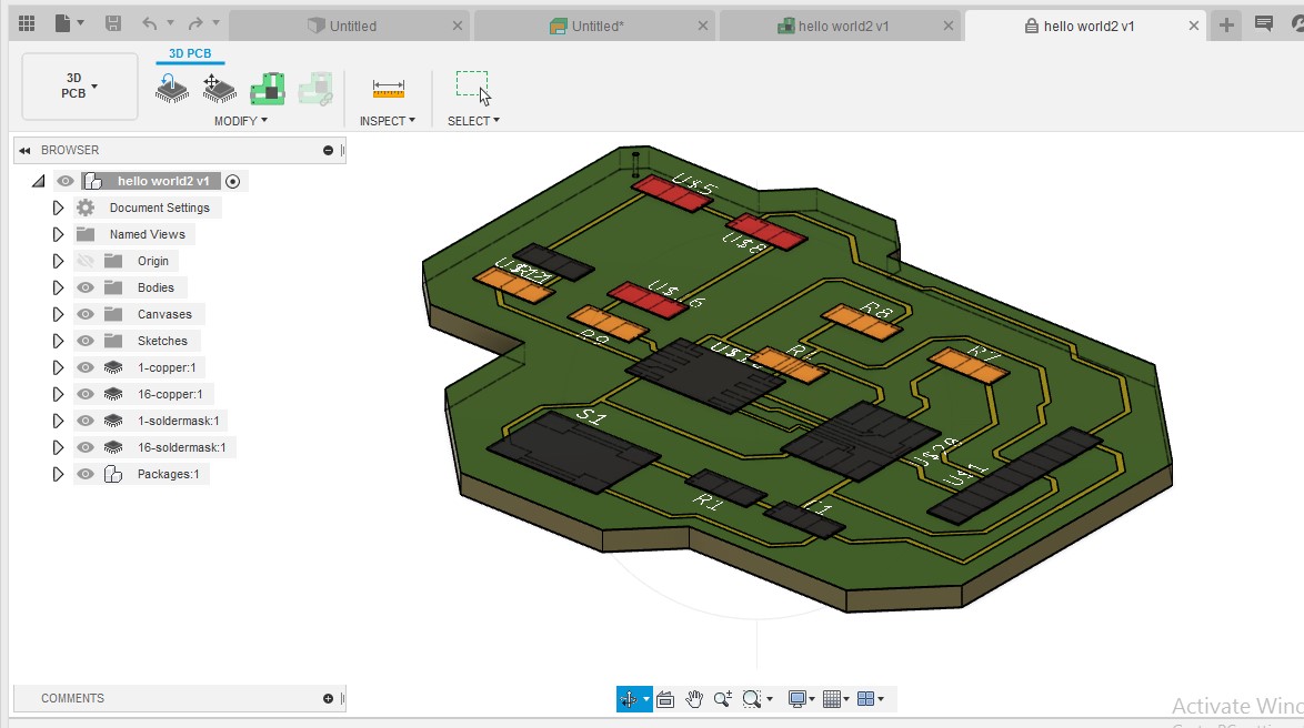
3D view
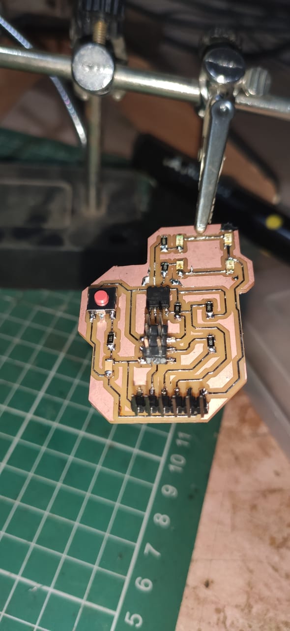
Components and Soldering:
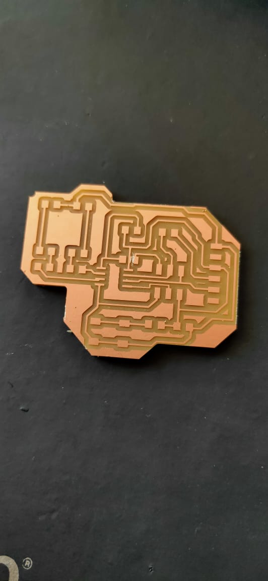
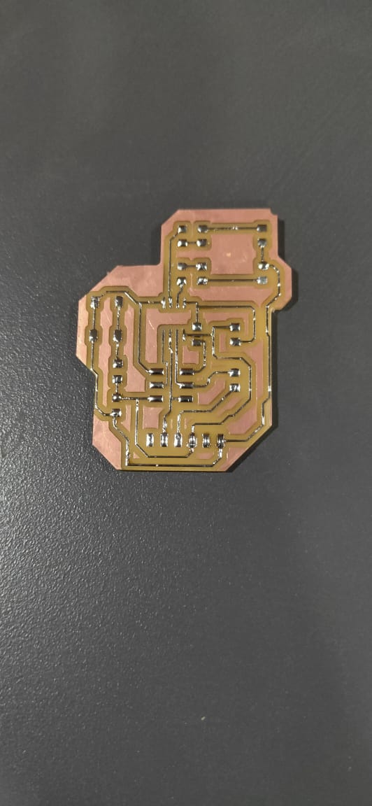
After designing we need to mill your pcb board.For that we are using SRM-20 machine.SRM-20 requires .rml file ,so using mod I have converted png file into .rml file.That file is given to machine and according to my design my board is milled.
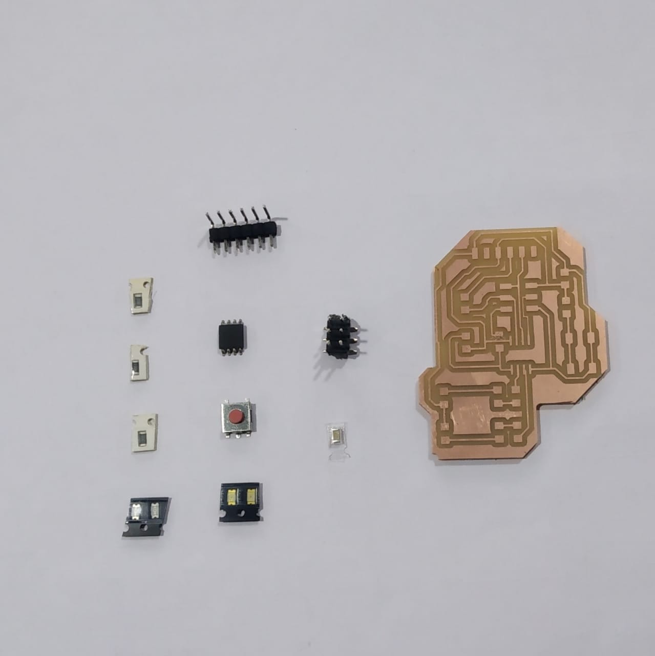
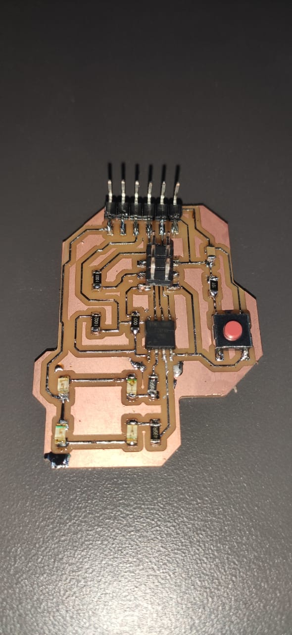
As neil given pcb image ,we know the components and its value.Neil told that add switch,led and resistor.Resistor is required to limit the current flow or avoid damage of led because of extra current.To calculate the value of resistor I have used ohms law i.e V=IR. We can get the current and voltage value from datasheet.so I=30mA and V=5V .Apply ohms law we get resistor value as 499ohm.I have used following components:
Capacitor=1uf
Resistor= 1Kohm ,10kohm
IC=Attiny45
Switch
LED
Pin header
|
|
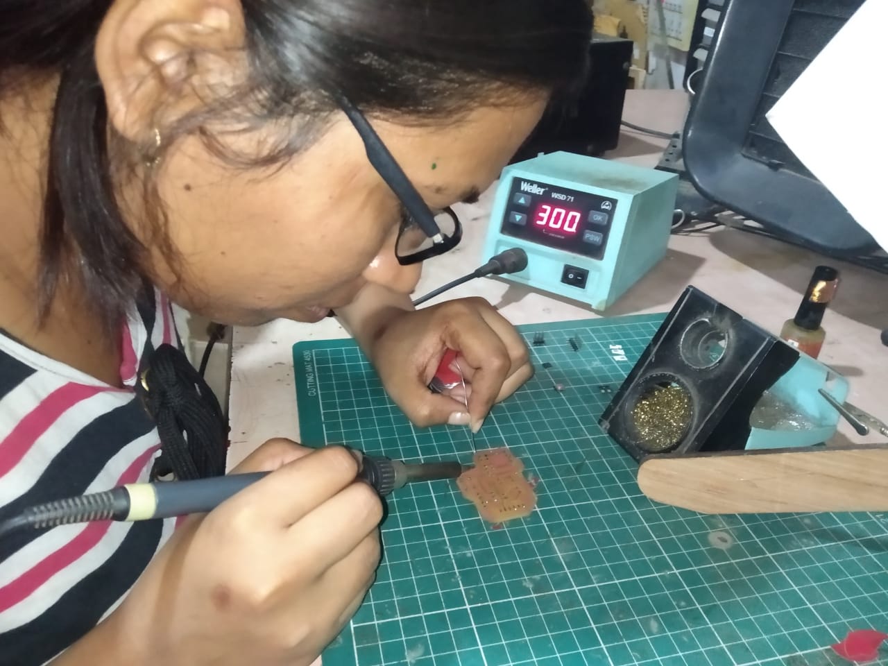
I have taken all components from fab inventory.I started with soldering .To make good soldering I have applied flux and did tinning process. After that I soldered all components one by one.
|
|
Now its time to test pcb is soldered properly or not.So I checked continuity using multimeter.Its working fine.
|
|
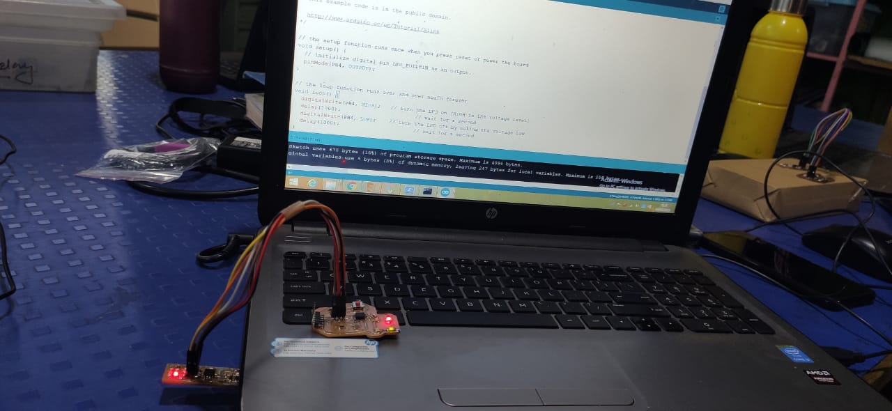
Programming Echo Hello World:
Neils has given programming steps for attiny 44.And also he provided echo.c and make file .I am using attiny45.I have downloaded both file in folder.I followed that documentation.I started programming my board using my ISP.I run first command make -f hello.ftdi.45.echo.make. This will generate hex file.
Program1
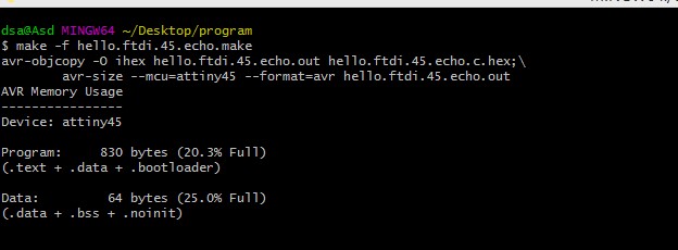
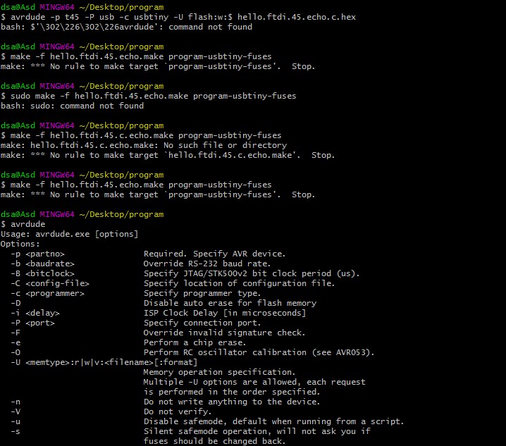
make -f hello.ftdi.45.echo.make program-usbtiny-fuses.This command is for make fuse .But I got error in this command like no such file or directory found.I told my instructor about this and he told me there is some issue in make file .
program2
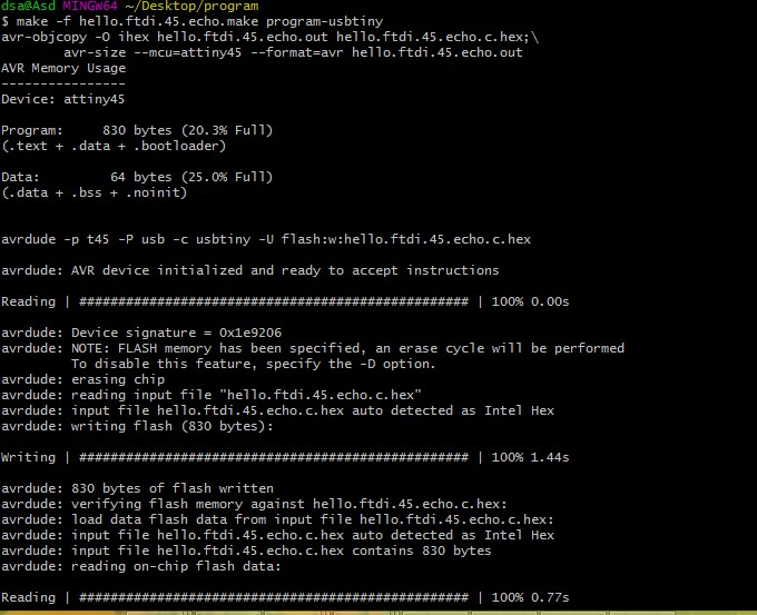
Now third command make -f hello.ftdi.45.echo.make program-usbtiny is for addition of program in your board.This command is working properly.Now we have to see Message which we have typed .For that we required python in your pc.If you dont have python ,install python.After that connect your board to pc using FTDI cable.But this command is also not working in my PC .It showing some garbage value.
program3
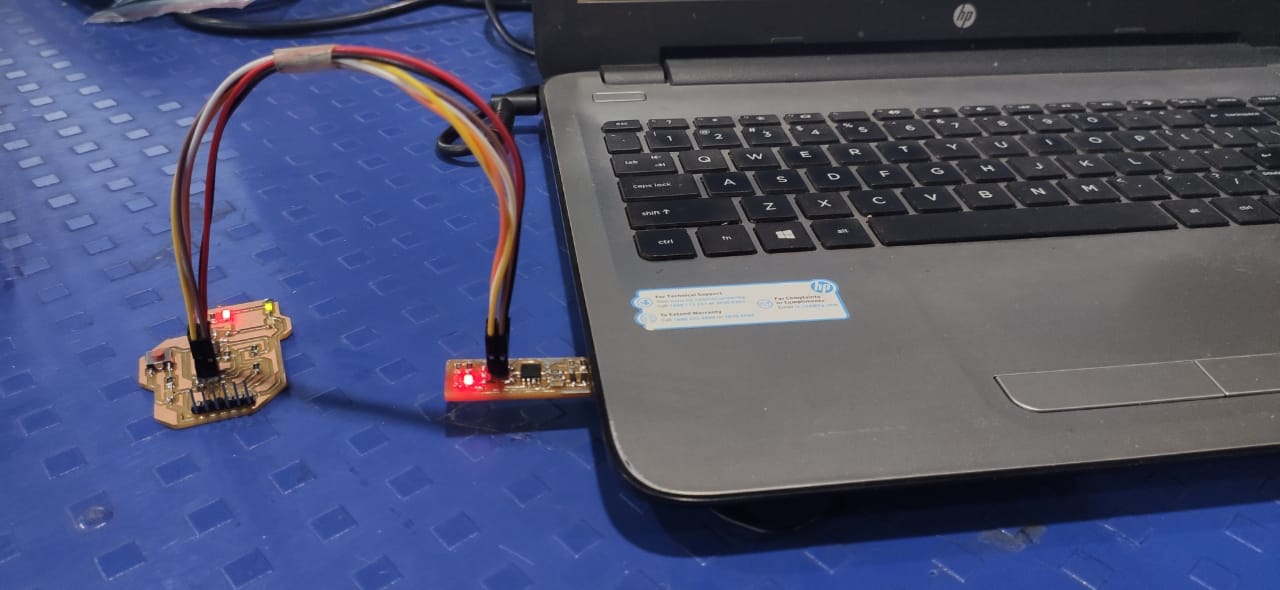
To check whether the board is working properly or not I have used arduino IDE.I have programmed my board using ISP.I uploaded blinking program.
Output
Group Assignment:
In group assignment we have to test different test equipment like multimeter,power supply,oscilloscope.So for that we have tested Nikhil's pcb.On power supply we have tested voltage and current.
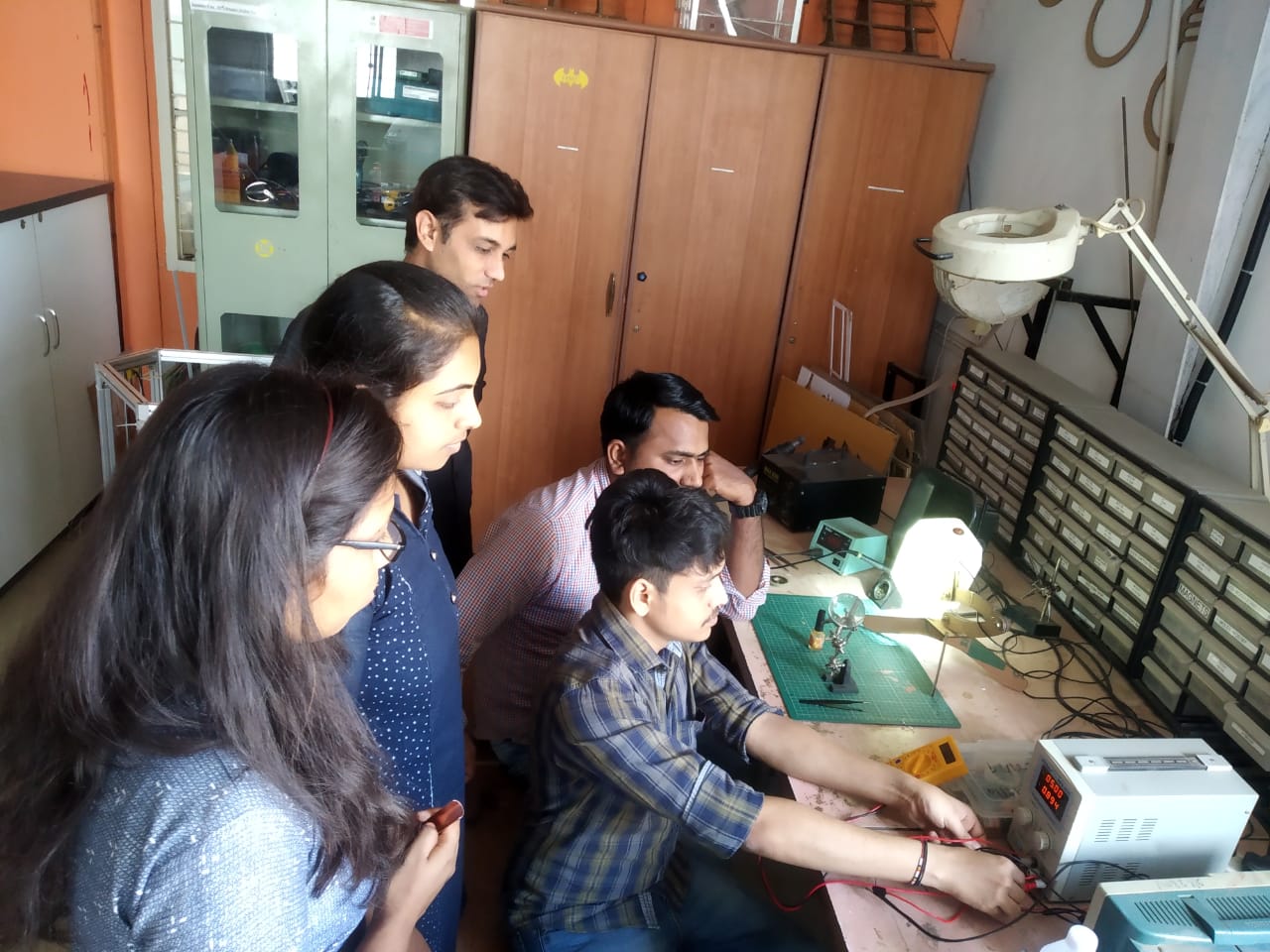
Power supply testing
On multimeter we have tested continuity ,voltage,current,resistance of our board.We can measure different parameters using multimeter.
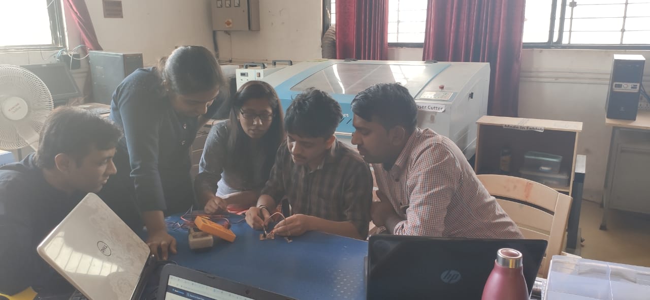
Multimeter testing
Learning Outcome:
In this week I have learned many things.I have learned different softwares like eagle,kicad,easyeda.Also I have learned how to debug our pcb.How to program our board.Also I have used different test equipment.Most important thing is you required patience for debugging your pcb.And also soldering should be very proper.
