Redraw Eco Hello world board by adding at least one input and output using " Autodesk Eagle" software.
Redraw Arduino (ATmega328p)
Using another software to do the Schematic and Layout.
To design the PCB I used Autodesk Eagle, which is electronic design automation (EDA) application, to design schematic capture, and PCB Layouts. Moreover, EAGLE stands for Easily Applicable Graphical Layout Editor.
It’s important to start the PCB design with schematic rather than jump straight way to the layout, having a nice and neat schematic will let routing the board easier. Therefore it’s important to have an idea of how the PCB will look like, so I must use the data-sheet of the microcontroller from the pinout diagram. I will know where to connect the inputs and outputs.
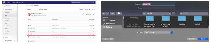
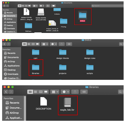
First of all, I added the Fab library that includes all the components I will need and that are available in the Lab.
.lbr extension, then I’m able to add it to Eagle libraries and save it.
Documents > Eagle folder. Inside it, there will be a folder called libraries, open it and then move eagle_fab.lbr to it.It’s important to move not copying it otherwise it will not appear in Eagle.
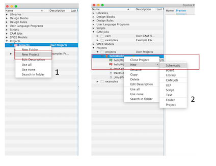
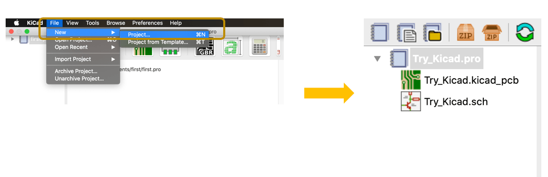
To start I created a new project then select New> Schematic as shown in the picture below:
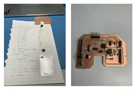
Used Components:
I did add:
To find the limiting resistor value I applied ohms law as shown:
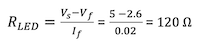
I used the green LED 1206 datat-sheer to get the LED voltage and current values, which equal to the forward voltage and forward current.
As shown from the above equation, the resistor value equal to 120 ohms. I can use this value or bigger, and as the smallest available resistor value in the lab is 499 ohms so I used it with LED as a limiting resistor.
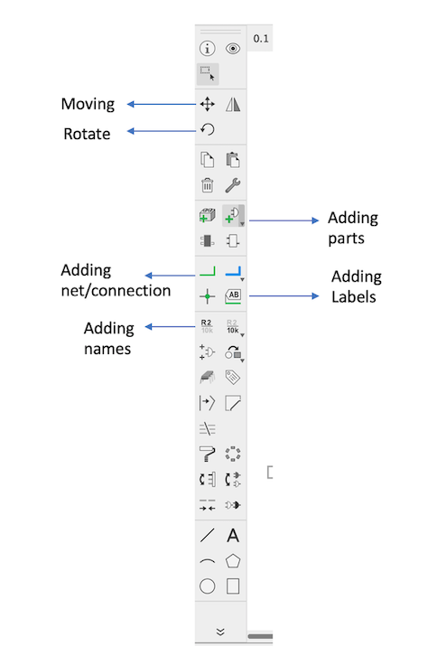
All the controls in Eagle happen by using Command Toolbar, the image below shows the functions of the necessary symbols:
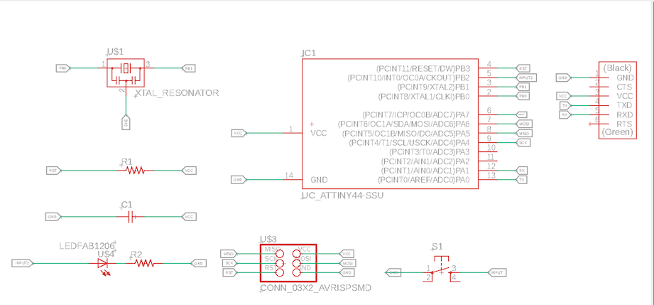
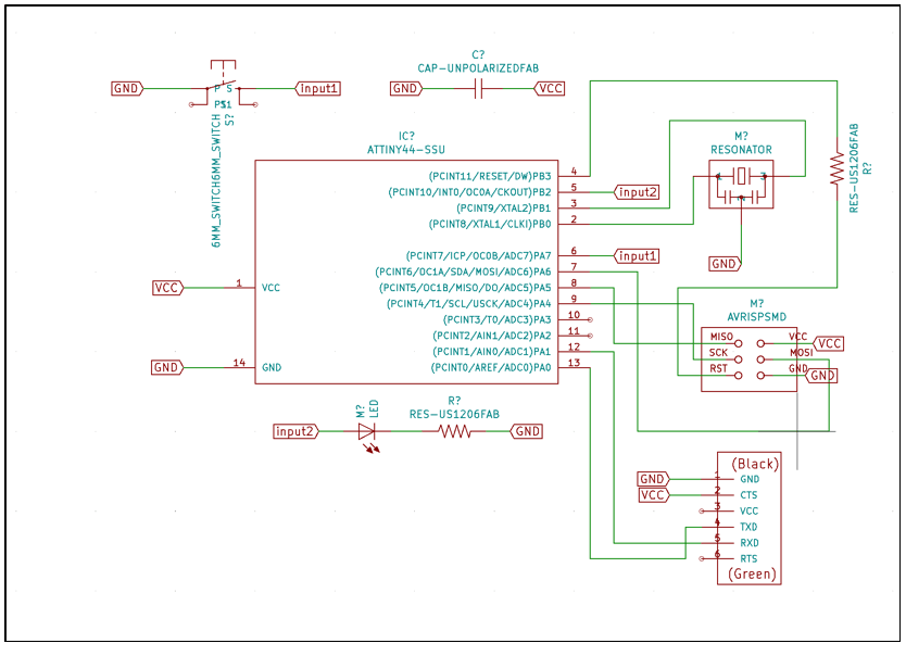
The image below shown my final schematic, I redrew Prof. Neil echo hello world provide in fab academy website. here is the ATtiny44 datat-sheer:
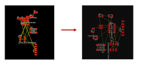
After checking everything are connected in the right place, I converted the Schematic file to the Layout file as shown below:

The picture below shows the generated board form the schematic with the airwires in yellow color, this connections needed to be routed, also as shown the components generated in random areas, therefore, I need to choose where to place them in the board then route them. Moreover, components placements very important, wrong placement may lead to difficult routing or impossible.
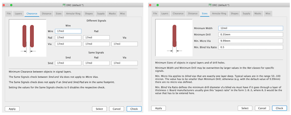
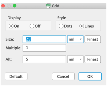
In addition, it’s important to review the design rule check (DRC) before routing, I changed the clearance to 17mil to match CNC machine settings and I did set the width size of traces to 12mil instead of 16mil which let me able to have more spaces where the tracks can go through, also I displayed the gird to help me in layout the components and to enhance the routing.
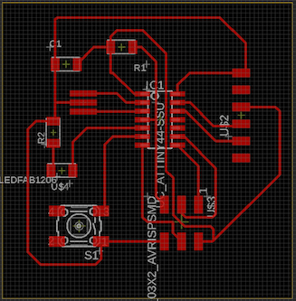
The picture below shows the final layout:
As shown below the steps of exporting the layout to images, to use them afterward in fabmodules:
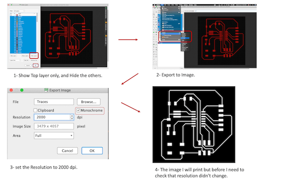
Next, I needed to check the resolution of the PCB images, and it was scaled to double the size, so I scaled it down by 50% to get the original size by using Preview as shown:
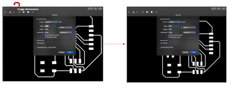
If I converted the image in fab modules with the wrong scaling I will have some problems while milling and the machine will not mill the compatible size.
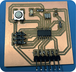
The video below shows the board is working:
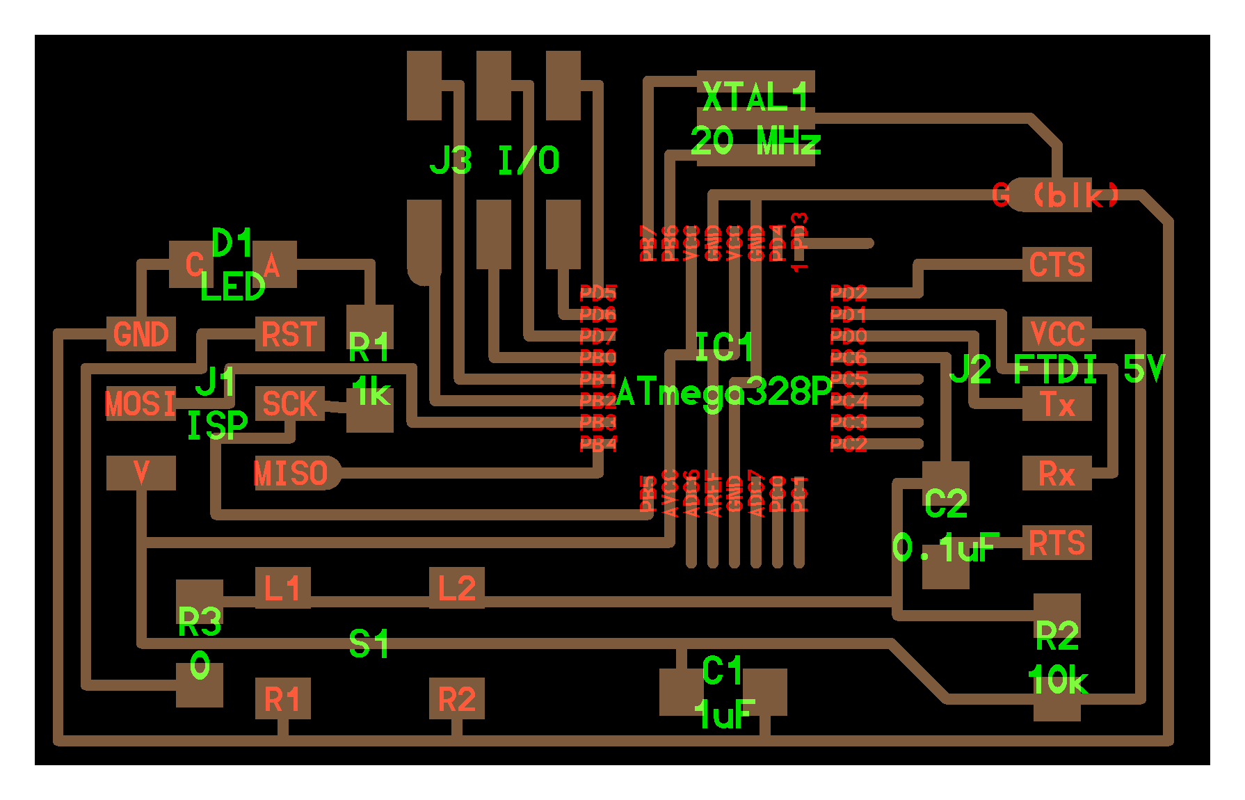
When I redrew the ATtiny44 hello-world board, I added only one simple input and output. For this reason instructor Hashim advice us to redraw ATmega328p with more inputs and outputs to use them in the coming weeks.
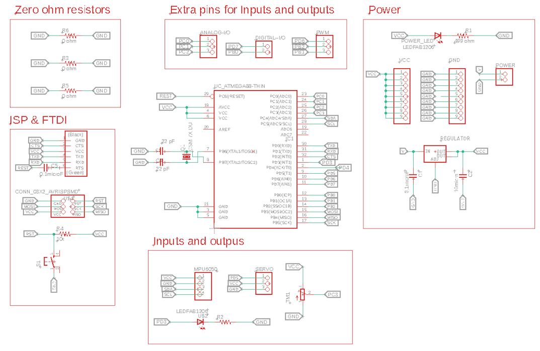
I started by redrawing the provide design for ATmega328p available in fab academy website, and I decided to add:
Servo motor. (output)
LED. (output)
MPU 6050 sensor. (input)
Potentiometer. (input)
I liked how my colleague Maha organized her schematic by adding blocks and naming them, I think this lets the schematic looks more clear and easier to read, so I organized my schematic similar to her
The image below shows my schematic diagram for ATmega328p:
To start with, I converted the board from schematic to layout, next I placed the components, this step took most of the time of preparing the board, to have the best placement to make the routing easier, An old saying is that PCB design is 90% placement and 10% routing.
I used auto routing for this board, auto routing is the process of getting the PCB software to route the tracks for you, it’s really nice tool but we need to use it correctly, it can produce a complete mess, its handy when having complex boards with not much routing space, However, we never use an auto router to do the complete board, after running auto route they’re some modifications we need to do it manual.
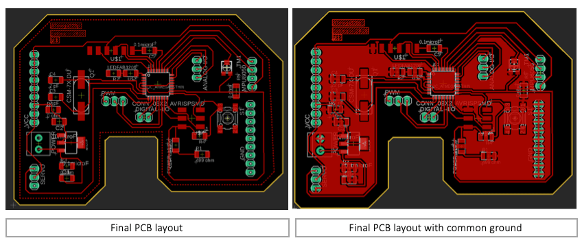
In addition to that, I added a common ground for my board. After I did the auto router, I un routed all the components connected to the ground and follow the steps below:
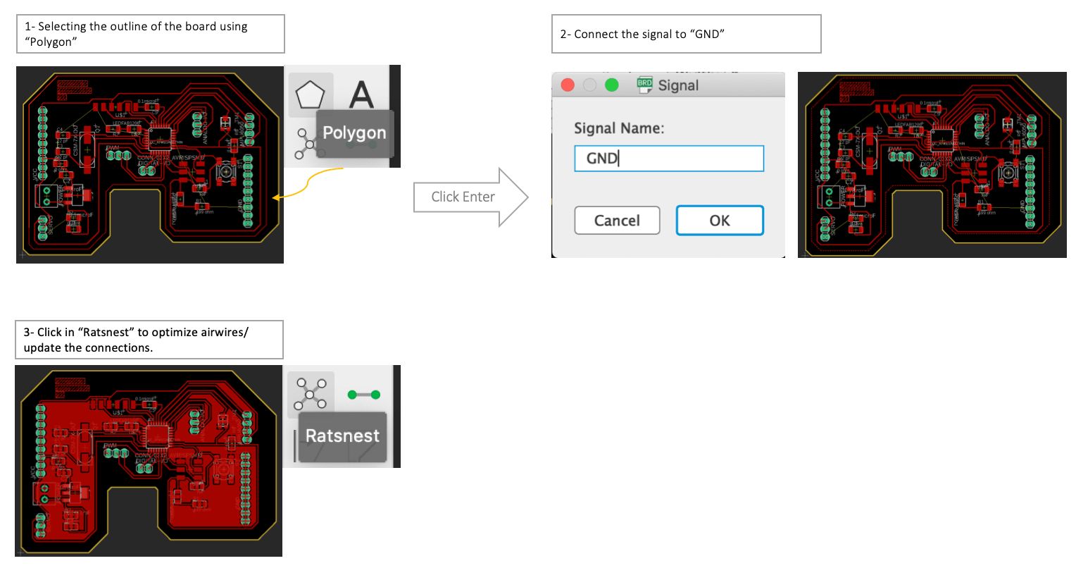
The common ground makes routing easier as we reduce the number of tracks, although sometimes some areas get blocked from getting to the common ground, this is known as an “island”, I had some of the islands in my layout, I did some work to remove them by changing components and track places.
As usual, the final step to check DRC and fix the errors if their is any, finally, the final layout shown below:
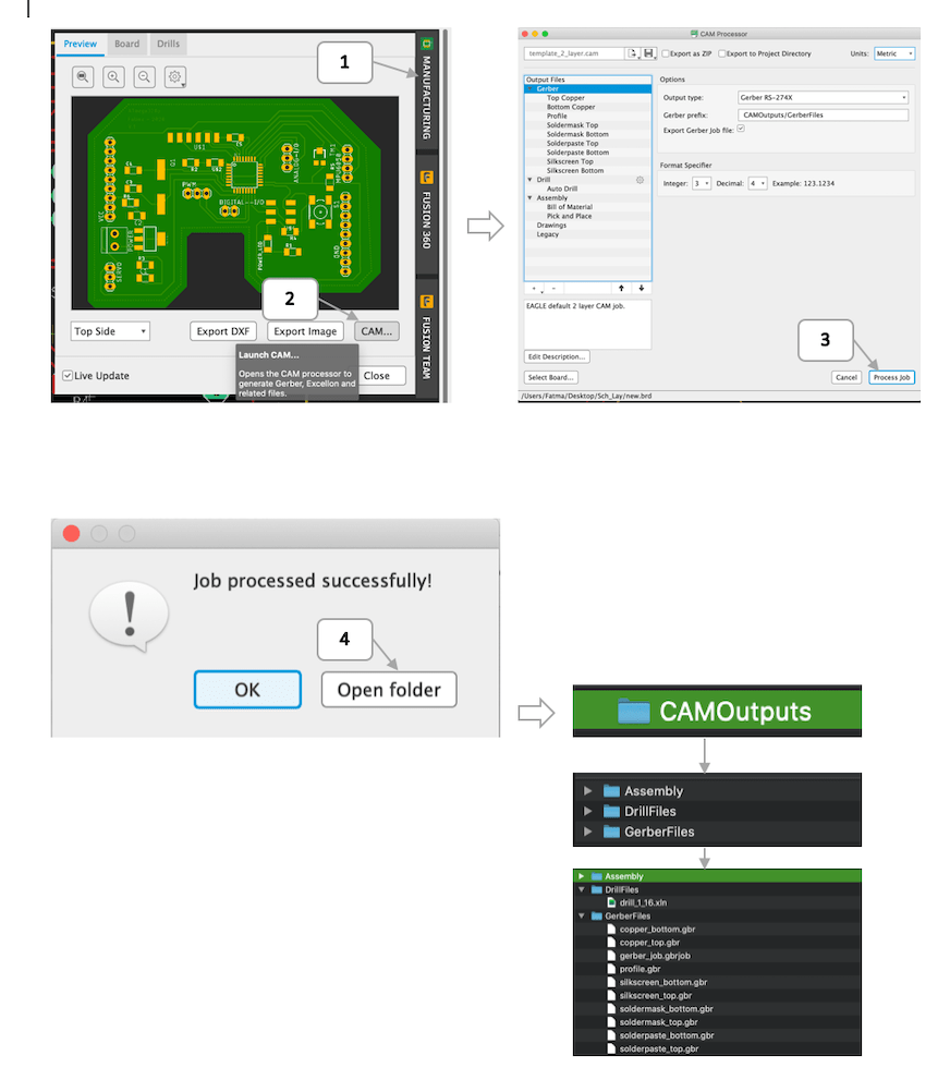
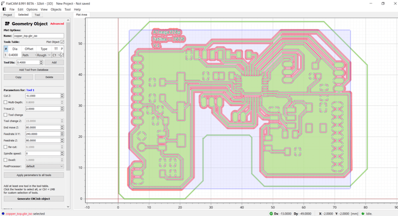
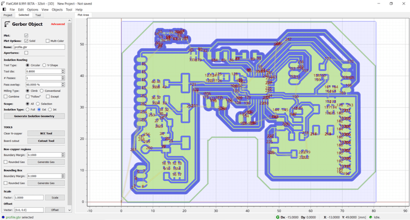
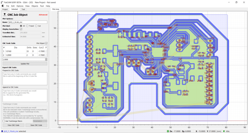
For this time to prepare the files for milling, I used FlatCAM it’s an open source software, which can open Gerber, excellon or G-code, and edit or create them from scratch, and output G-Code, also Isolation routing.
I got Gerber file from eagle instead of getting the PCB images, those are the steps of getting the Gerber files are shown below:
Due to some mistakes, I did while entering settings in FlatCAM I need to do:
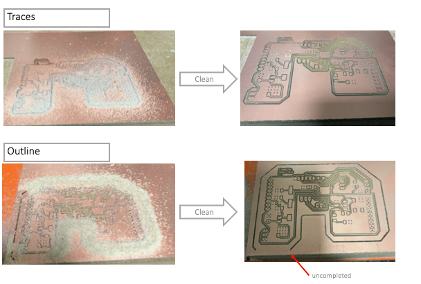
Manual cutting of the board outline there is a small part that didn’t cut, I used motor bandsaw minimax s45n the images below shown the steps: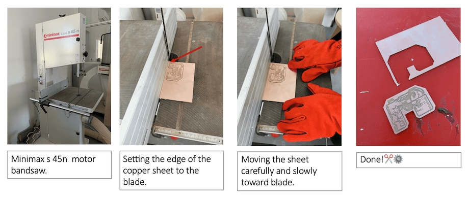
Drilling the through-hole pads, because the header’s legs can’t fit over the pads. I used the Dremel workstation: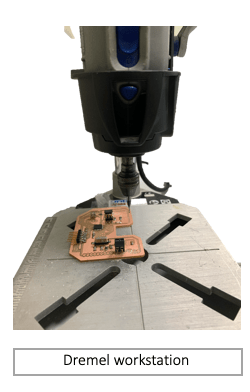
I had some problems while soldering ATmega328p. At first I was confused which soldering technique is the better to use.
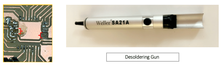
First, I applied a solder in all the pins .Then I used (Desoldering Gun) to remove the extra solder between ATemga legs, but it’s was not that easy. Whenever I tried to remove the extra solder ,I couldn’t remove it and I think I used the ( Desoldering Gun) too hard which damaged the board. Some of the pads removed as shown in the image below:
Fortunately, the pads that didn’t get connected to any pins only were being removed, so I tried to solder the chip one more time, but because of their remaining solder from before, which I could not remove , so it was difficult to align the pins with pads
Furthermore, on this day 15/03/2020, the lab was scheduled to close due to COVID-19.
Instructor Hashim advice me to mill another board as there is no enough time to fix it, and the board was damaged very badly, therefore it was impossible to fix it.
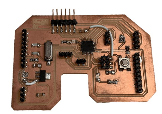
Second board:
For this time before milling, I fixed the settings in FlatCAM, thus there was no need to do manual drilling and cutting for the board.
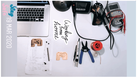
I borrowed from the lab soldering iron, some electronics components, that I may need to use for the following weeks at home.
Stay Home, Stay Safe!
After, I finished soldering, I started to check the board, first error I found was that there is a short circuit between VCC and ground, the problem was from the headers their was an extra solder connected to the common ground with VCC.
Next, I start to check the connection between all the pins using my schematic, I found another short circuit between the terminal and voltage regulator, I did de-solder the terminal, unfortunately I cut the pad by mistake, I needed to use an external wire to fix it.
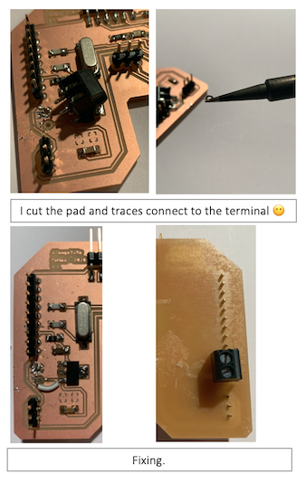
I soldered the terminal from the bottom because it’s was a little hard to solder it from the top, after the track was damaged.
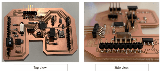
Now finally, the board is clear from short circuit, and all the pins are connected with the components in my board and I can start to program it.
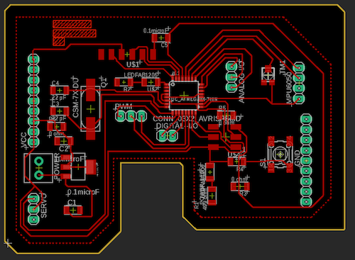
While I was trying to program the board I faced problem trying to burn the bootloader, the RST pin in the ISP header wasn’t connected to the MCU, so I added another external wire to fix the connection. Moreover, I fixed this connection on the eagle design, for further use in the future if needed as shown below in the updated layout.
For more details visit embedded programming week.
The video below shows the board is working:
In my undergraduate studies, I was using another software called DipTrace. In fact, I liked DipTrace more than Eagle, the reason was it was easier to use, it’s quick and efficient in creating board, also I can use it without wifi.
In addition to that, I tried to use it in this week assignment, but I couldn’t open the software even though it was already installed on my laptop. To fix this problem I opened DipTrace software website, the problem was that DipTrace has not supported macOS 10.15 Catalina version anymore, which is the version I have on my laptop.
Is a free open source software, suite for Electronic Design Automation (EDA), used to create schematic capture, and PCB layout with gerber output and other output formats.
I was searching for tutorials to help me use KidCad. I followed this guide done by Barcelona this one was the best for me as it easy and clear to follow.
First, I faced some problems adding the library, I was using the same library I used for eagle, In fact, I needed to use library formatted for KiCad, I downloaded the fab library - fab.lib from this link, the steps bellow show’s how to load the library:
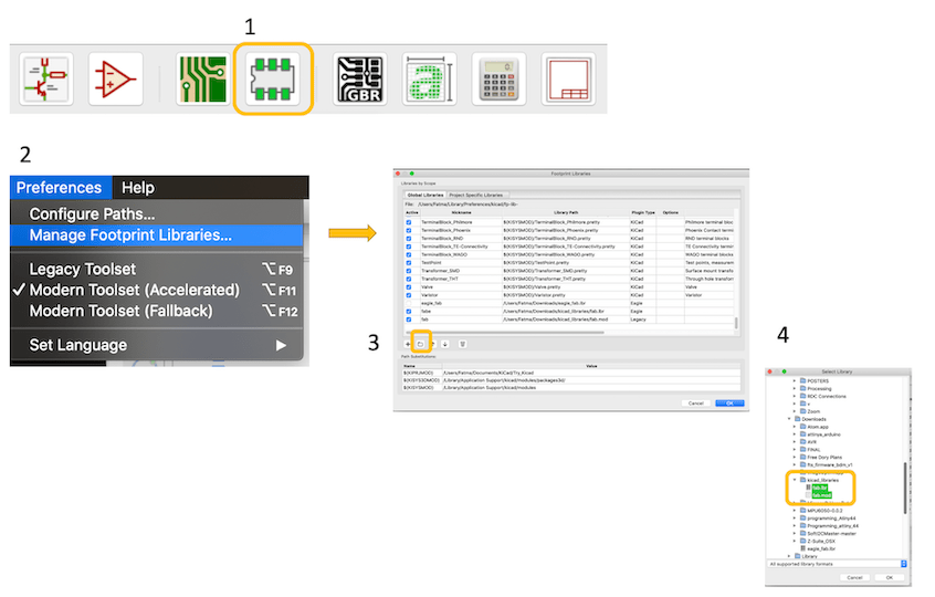
To create schematic, first, we need to open eeschema, all the tools are smilier to eagle toolbar but in my opinion, it’s easier and handy in KiCad.
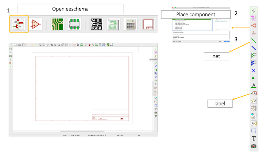
I used the same design I made of the (ATtiny44 hello board) for learning purposes because I only wanted to try to use KiCad.
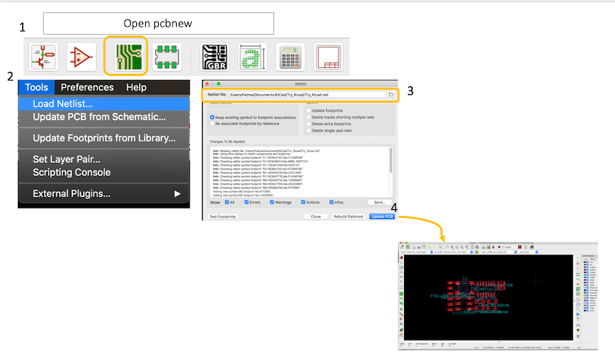
In KiCad before starting routing we need to create Netlist, which will be saved automatically at the project folder.
The first thing I did when opening pcbnew , is to load Netlist as shown in the image below, after loading it, the components from the schematic appear and are ready for routing.
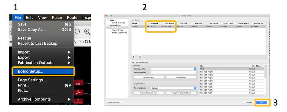
As usual before routing we must check the board setup –> DRC, I used the same settings as used in eagle, 17 mill (0.4318 mm) for clearance, and 12 mill (0.3048 mm) for Track width as shown:
The video below shows the process of routing the board:
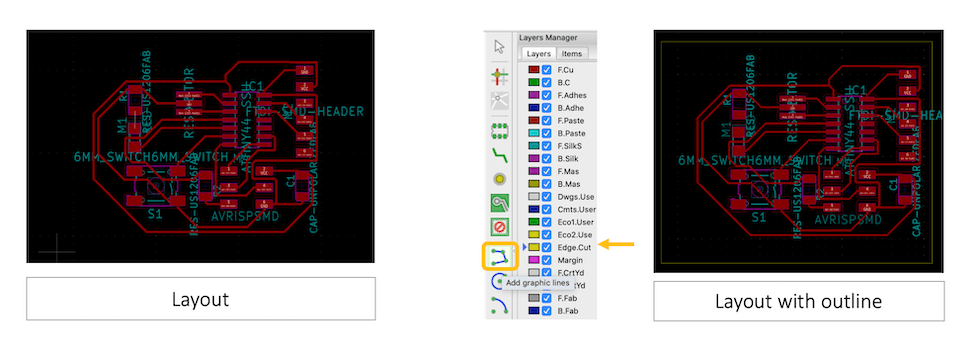
The images below show the layout with and without the outline. To add an outline I used Add graphic line, and change the layer to Edge Cut from Layers Manager, then I drew the outline around the components as shown below:
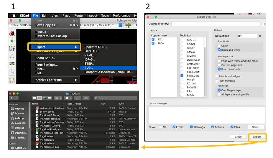
Finally, the last step to any PCB design is to convert the PCB to formats understandable by the CNC machines, the images below show the export steps:
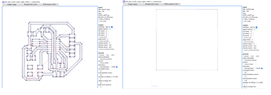
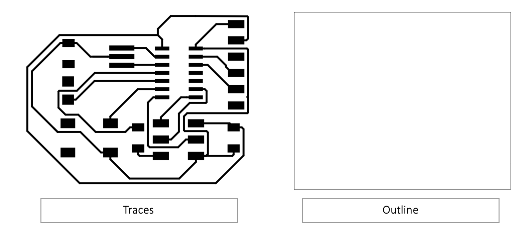
The image below shows the Traces and outline ready to mill:
| Files | Link |
|---|---|
| ATtiny 44 schematic & layout - Autodesk eagle | |
| ATemga 328p schematic & layout - Autodesk eagle | |
| ATtiny 44 schematic & layout - KiCad |
