First simple steps into electronics design by recreating an example board and adding simple features.
As a small preamble this week it was my turn to showcase current development: stressful but insightful. #done
 – The Review –
Overall mastering electronics, personally for me, was one of the main goals in signing up into FabAcademy overall so this week was very exciting for me. The world of electronics is a mysterious jungle for me. I have had a general understanding of what happens physically, but the jargon and the specific tricks escaped me and created a lot of confusion. This still unfortunately stays this way, but at least it doesn’t inflict intimidation when I work with it. After going though main types of components in circuits first with Neil in common lecture and then locally again it became more clear of what is used for what. Hopefully with practice this knowledge would get settled in my mind. Overall the process went rather smooth. The biggest challenge was to keep track of which types of components and which footprint apply for the components that the lab has.
Process
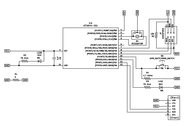
To design (or rather redesign) I used KiCAD following local FabAcademy example and a more complex tutorial here. After messing around with different boards and chips from the list, I decided to go classic and simple but to understand all parts with the ATTiny 44.
.jpg) – KiCAD Project –
– KiCAD Project –
In more details I went through the following steps:
-
Install software and libraries for schemes and foot-prints during a local demo;
.jpg) – Software Libraries –
– Software Libraries – -
Recreate the original schematic and corresponding foot-print;
.jpg) – Initial Schema and Footprint–
– Initial Schema and Footprint– -
Add an LED on power;
.jpg) – chema and Footprint with LED on power –
– chema and Footprint with LED on power – - Consulting the datasheet of the chip on the function of the pins, add an LED as an output and a button as an input;
-
Correct wrong components with incorrect footprint, fix button to be linked to ground not power (facepalm), add a pull-up resistor, adjust resistors for the inventory;
.jpg) – Resulting Schema and Footprint –
– Resulting Schema and Footprint – -
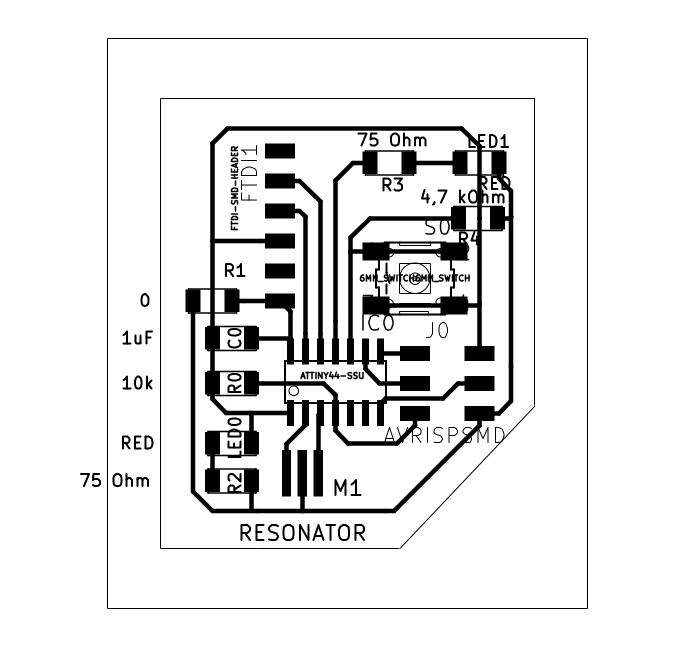
Extract .SVG files and convert them into .PNGs;
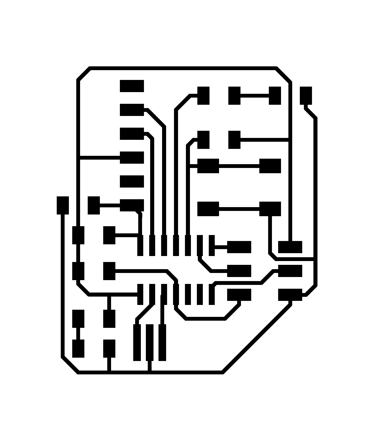 – Resulting Trace Cut File –
 – Resulting Outline Cut File –
 -
Create the .RML files with Mods and fabricate the board;
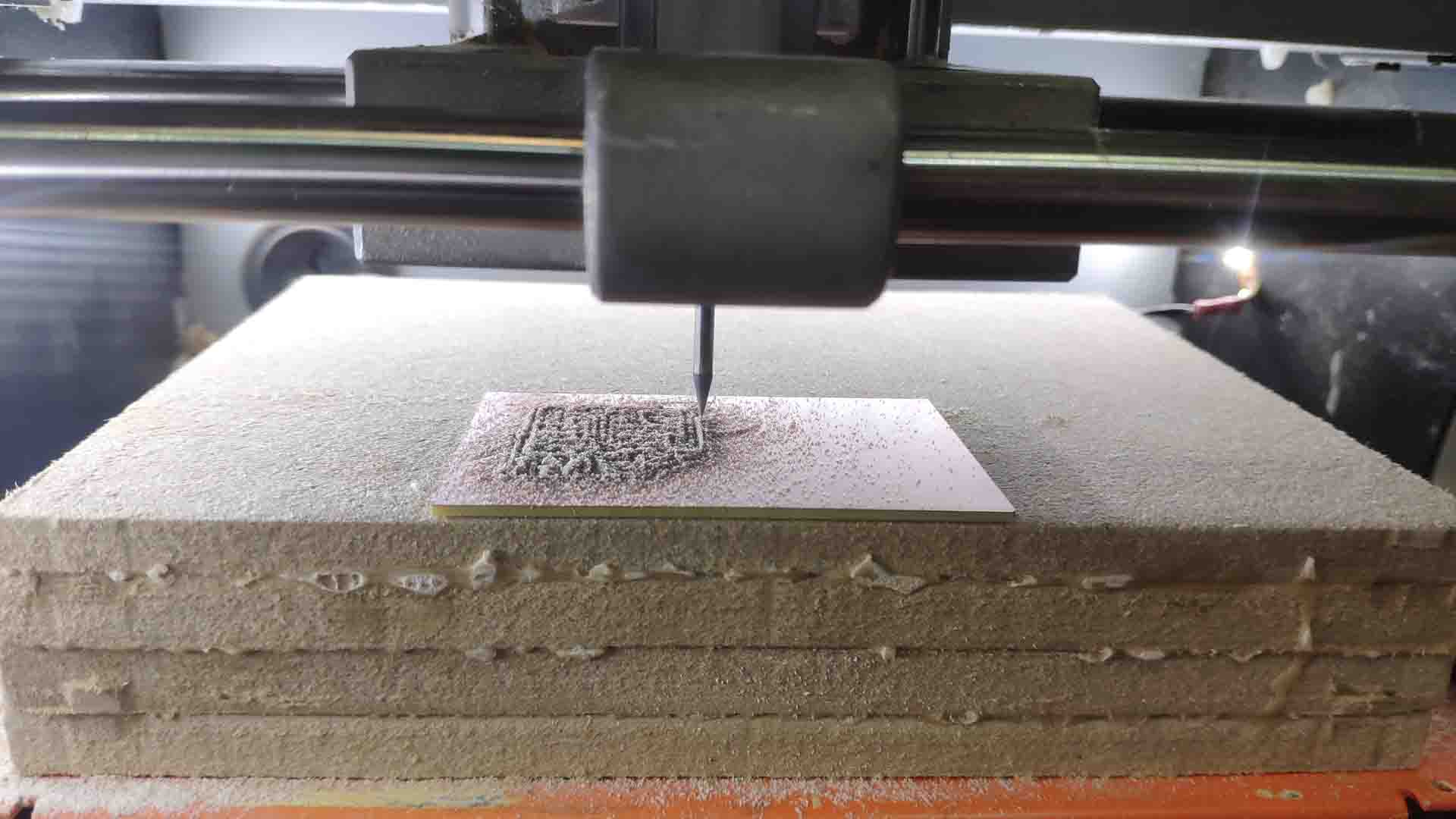 – Cutting the Board –
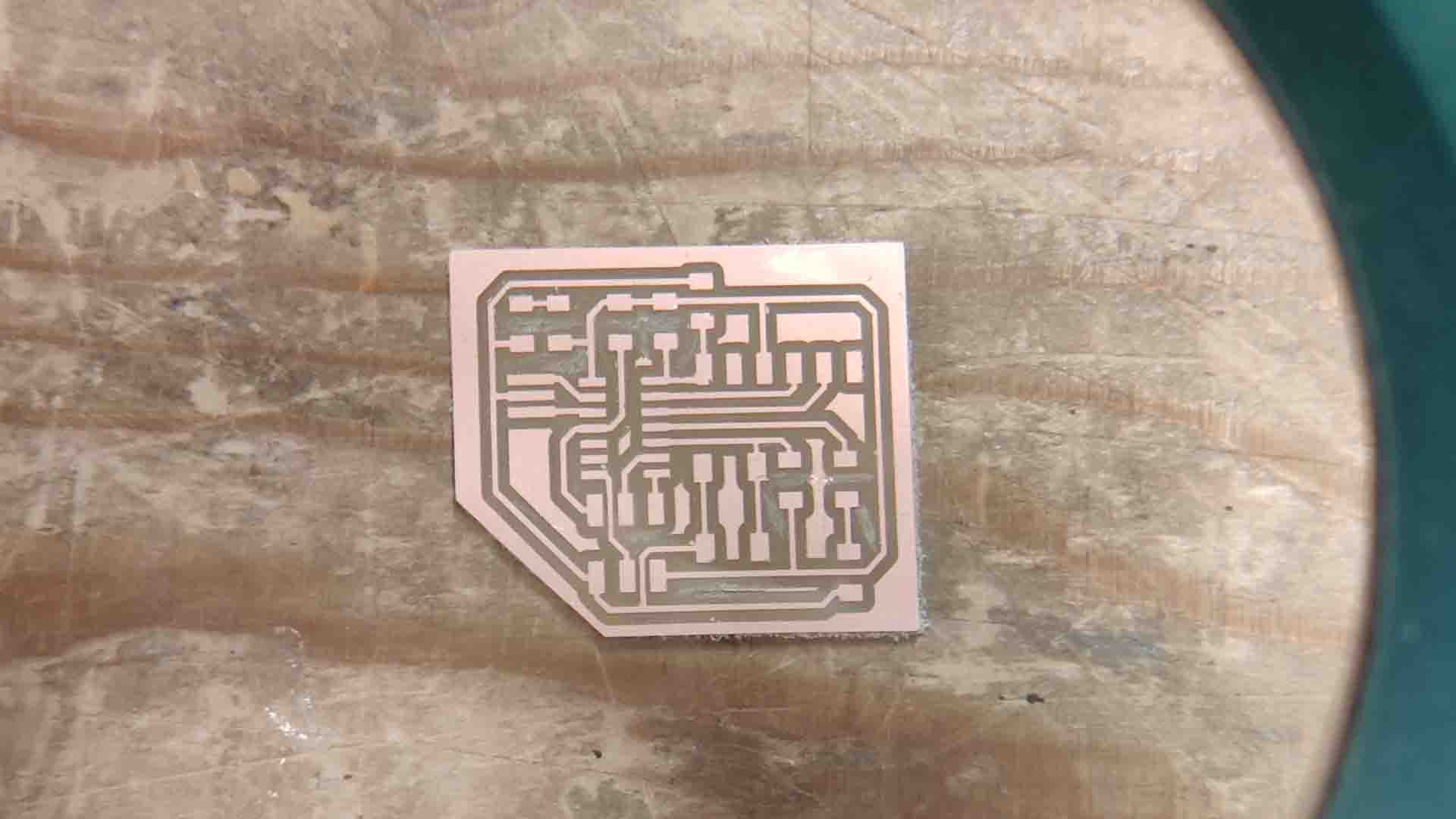 –Resulting Board –
 -
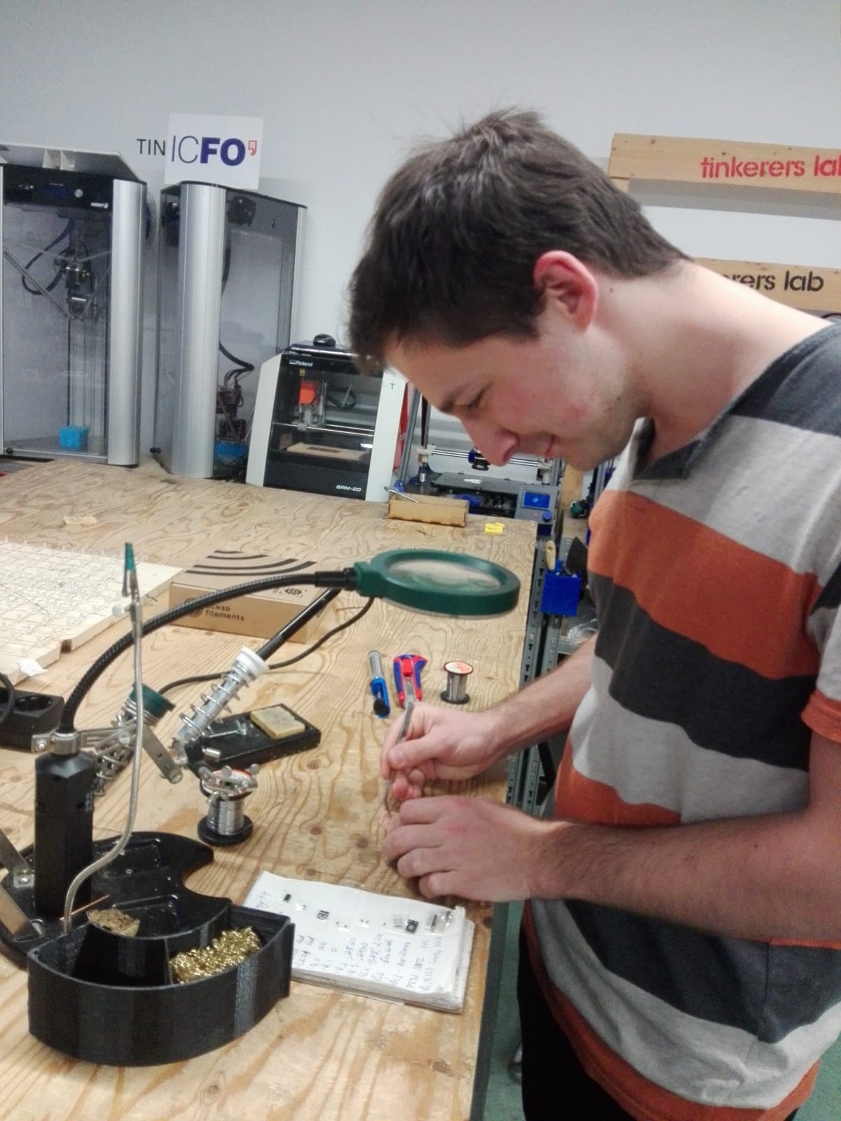
Solder the pieces, test connectivity.
 – Shopping List –
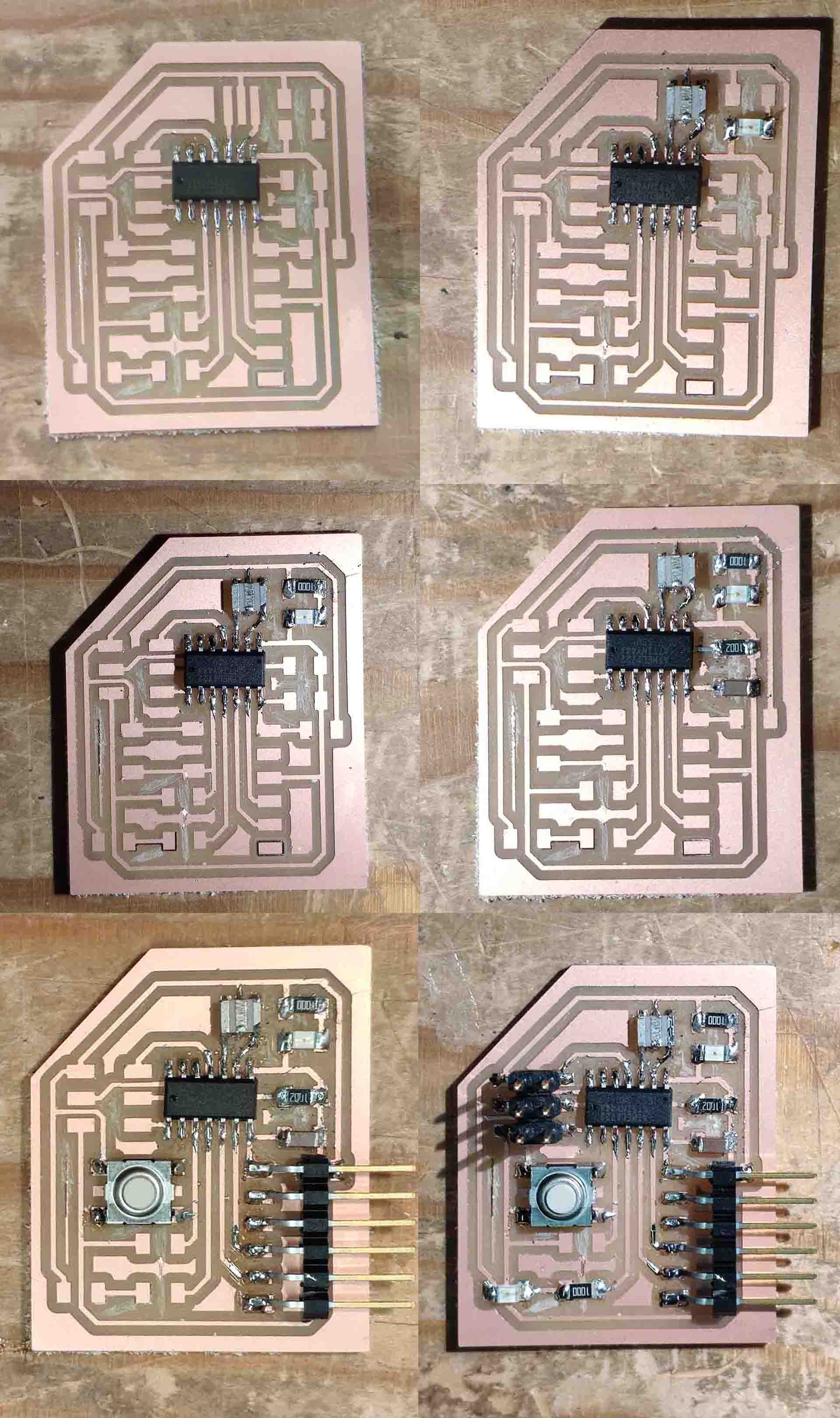 – Soldering Process –
Lessons learned
Personal discoveries of the process:
 – Soldering Process –
In general on Electronics:
- After messing around with various simple prototypes with Arduino following local extra class, I realized (or understood) that LEDs require a resistor so that the current doesn’t get too big with the minimal resistance they have and same voltage of the network. However, it is not as fixed: if the resistance is bigger, obviously the current would be lower thus the brightness would be lower. Moreover, different color LEDs would have different forward resistance and slightly different optimal current, thus RED ones, for example, require lower resistor (75 Ohms) and green ones - higher (up to 170 Ohms). To calculate initially the necessary resistance I used this link and the datasheet and with the data from there (namely forward voltage and optimal current) used this calculator to arrive at these values.
- Resonator serves as a quicker and more reliable clock than the one built in to the chip. It is not strictly necessary but it helps to maintain functions synchronized.
- Capacitor should be close to the microcontroller so that the signal is filtered as clear as possible;
- A button as input requires an additional resistor 4.7-10 kOhms of resistor to power to avoid ambiguous signals in state between high and low of the button. This article cleared it a bit more for me.
On Schematic:
- When working with the initial schematic it is useful first add all components and than try to spread them in such a way that each is in it’s own zone. Also I tried to recreate everything at once and got a lot of confusion - it is better to start from simple steps.
- It is better to do a draft out the schematic - and once it is clear what is connected to what beautify and arrange it. It also helps in preparing to layout the footprint.
- After confusing some parts I understood better the concept of packages - various implementations using same piece. In that it was interesting to read more on difference between Small outline integrated circuit and Quad Flat No-leads package. This article on Surface Mounted Device was also extremely illuminating and removed a load of confusing abbreviations.
On Footprints:
- When designing the circuit LEDs, resistors, capacitors can be used as bridges. In my case I used extra 0 resistor to jump over a line.
- Additional trick to use was to use area under big components like the controller itself or between the pins for connectors. This allowed for less routing. The only thing to keep in mind is the width of the traces should be kept in mind so that they don’t get connected because the bit cannot pass between them.
Conclusions
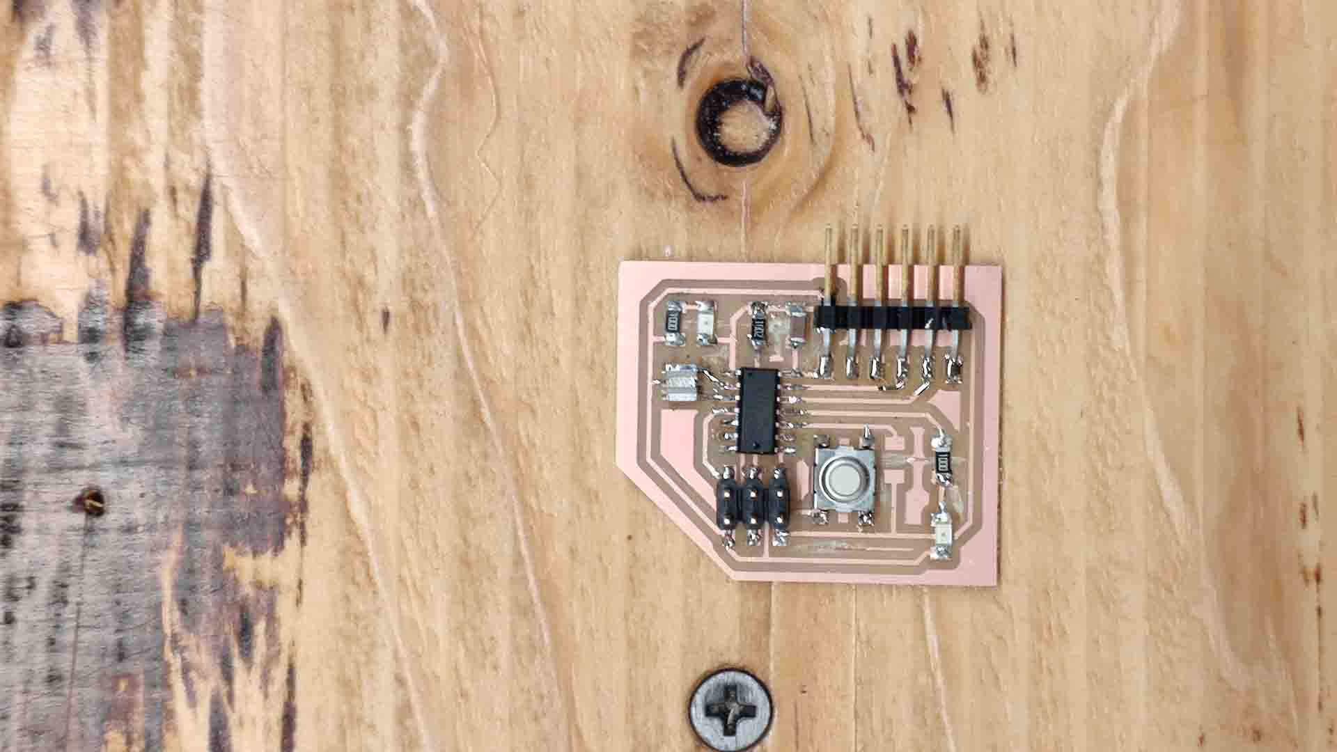
Overall result is by far not optimal (just adding two LED with the two resistors and a button with a resistor) the board went from 27,9 _ 26,1 mm in the example to 39,75 _ 47,4 mm - 1,6 times bigger. Obviously this can be optimized but for the first time it is not bad. Plus it made already intricate task of soldering slightly less daunting. However, I can honestly say that this piece of electronics is made by me and I understand much more what it does and what can be done with it.
 – Result –
As future steps I want to try out the python library mentioned by Neil, for descriptive coding of circuits and subsequent auto generation.
Post Scriptum
After debugging session in my input week I found an error in a way I connected a button in this design. It should be in reverse.
Here are the corrected traces:
 – Schematic of Logic –
 – Schematic of Traces –
 – Inner Cut –
 – Outer Cut –
Work File:
Batteling ESP-32
To get into built in networking as well as aiming for thepower of the chip I started to look into ESP-32 chip.
To start off I whought I would try first to even get an on board LED of this board the Lab of Barcelona prepared for students.
 – Barduino –
I did manage to power up the board (power LED worked). I kept getting errors with a FTDI converter I made in the lab, which made me think that was a problem, so I had to order FTDI programmers to be able to move on and not waste more time debugging. Errors on Wywtem disappeared - amazing!
So using this tutorial I went ahead to code a simple program for it. LED was still not working.
I thought mabe there is something wrong with the process of programming it so I played with programming Baud rates in Arduino IDE, tried different boards. I also tried to program it using platformio linked to Atom text editor I am using (using this plug-in and following Platformio’s set up guide) and using this local tutorial to code using it.
Unfortunately nothing seemed to be working. So I began troubleshooting.
First issue I had was that I was having the problem where the code would upload every second time - I had to disconnect it or alter the baudrate for programming - I suspect that was because the ptogram I was writing had serial communication which would be sending thing and conflicting with writing new programs (?). Not having the capacitor I’m not sure if this will work but the problem they describe is the same so I want to reference this just in case to test later on. Similar with this as a potential solution (same approach described here).
After some very confusing and furstrating weeks of coming and going from it, I narrowed down the problem to the say I soldered the chip - because when I put external LED directly to the pins seemed to work. Unfortunately in the process of resoldering I manage to butcher the board so I am in a limbo for a while.
Thus at the moment I am redoing the board layout my self to get to know the chip better (which seemed to work for me when experimenting with the ATtimy 44 in previous experiment).
I started reading the datasheet for it, which rather confusingly is directing you to another general datasheet for the whole family for some info.