Electronics Design
Tasks for this week:
- Group- Use the test equipment in the lab to observe the operation of a microcontroller circuit board.
- Redraw an echo hello-world board, add a button and LED (with current-limiting resistor).
- Check the design rules, make it, and test it.
Part 1- Group Assignment
Due to COVID-19, our main lab was closed. So, we did not have access to an oscilloscope, and therefore were unable to complete this week's group assignment. This page will be update soon.
Part 2- Designing and Preparing a PCB for Milling
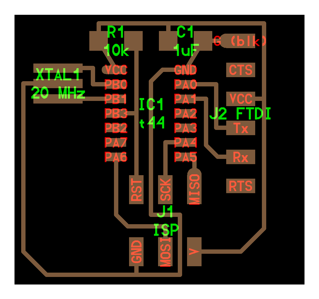
Our task this week is to design and produce a PCB, whose main function is to act as an echo board for transmitting and recieving between the computer and the microcontroller. As I will be using the ATtiny44, I opened the FabAcademy website and found the reference image that was provided for this board.
The next thing to do was to create a BOM (Bill of Materials), which is as follows:
- 1x ATtiny44
- 1x 2X3 Pin Header
- 1x 1X6 FTDI Jumper
- 1x 1uF Capacitor
- 2x 10k ohm Resistor
- 1x 20MHz Resonator
- 1x Button
- 1x LED
- 1x 499ohm Resistor
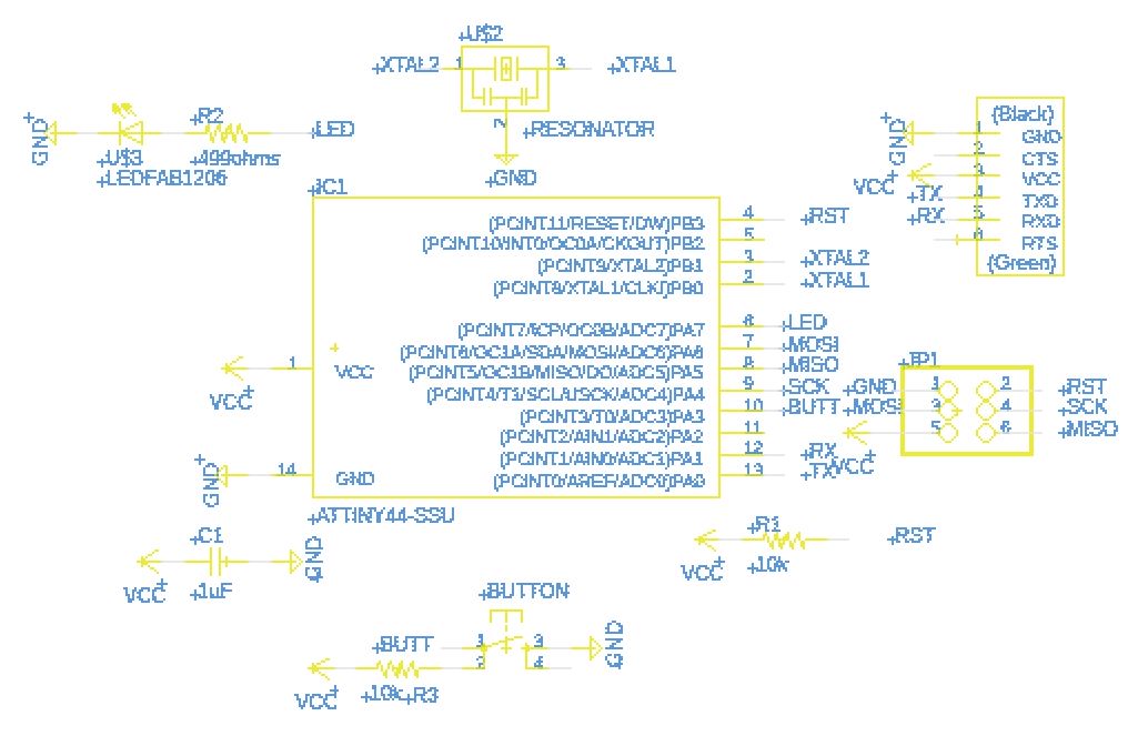
Then, I drew a schematic drawing of all the components, and adding the LED and button components. I started drawing in Fusion 360's integrated Eagle software, where I successfully drew the entire schematic and created all the traces for the board.
Error! - For some unknown reason, my Fusion 360 software crashed unexpectedly. When I re-opened Fusion, I could not recover the files- when I opened the recovery files, I still had the board design (.brd file), but that was useless as I had lost the schematic drawing for it (.sch file).
After this same incident occured with some of my classmates and my instructor, we decided to switch to the older, stand-alone version of Eagle. The tools were the same, and I grew comfortable with the new interface quickly. Another thing to quickly mention is that we installed a Fab Components library, which only included the parts relevant to this task. The process for doing this is to download the library, open the library manager in Eagle, then Use the Available library with the specific Fab components.
I started adding all of the aforementioned components. Using the Net tool, I drew extending wires from all the components, and giving the same name to the required connections meant that those components were now remotely connected. After re-drawing the circuit schematics, as follows:
I converted the schematic to generate a .brd file. Here, all the components were put together in a mess. So, I moved all the components to a corner, and started placing them in a compact manner than minimized space, closely following the reference image, and also adding the LED and Button components. To arrange these components, the first thing I did was change the grid to 10mil, which reduced the restrictiveness in moving the parts. Then, I also changed the Clearnance and Sizes design rules to 16 mil and 10 mil respectively. Now, my design will abide to the design rules of PCB making.
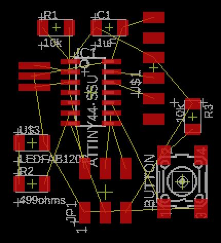
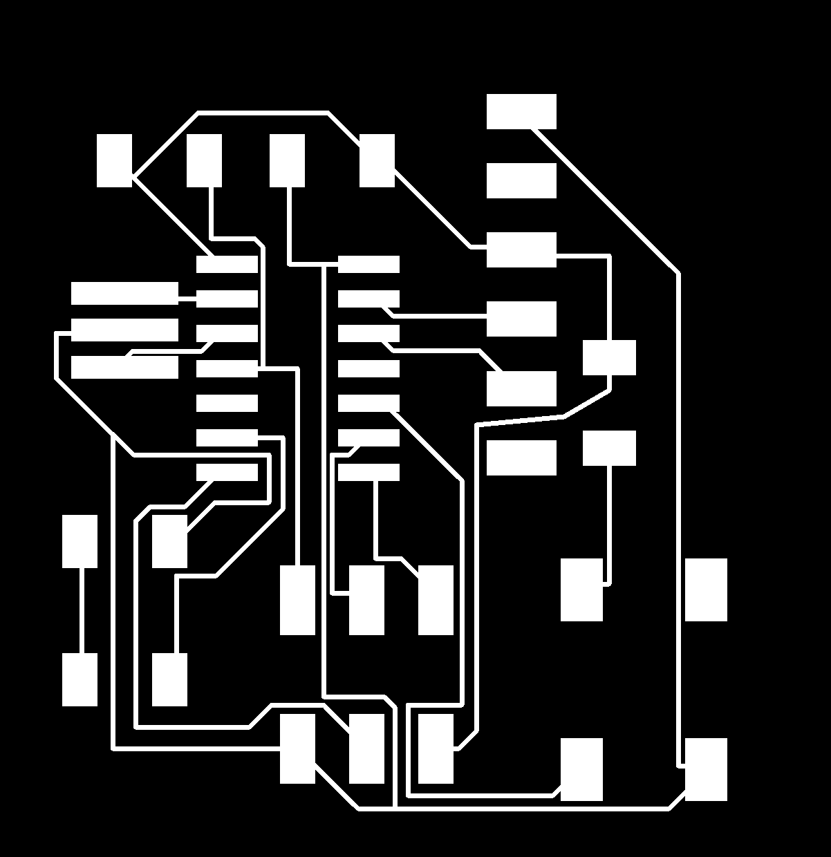
The next step was to create the traces for all the components of my board. Before doing this, I changed the size of the board to 32X32 mm. Now, whilst the traces can be drawn manually, I chose the Autorouter tool, where I ensured that traces would only be drawn on the top face. I ran the autorouter with High effort, then chose the shape that I liked best. Using the move tool, I closely inspected all the traces, and moved some to make sure that they were not too close together.
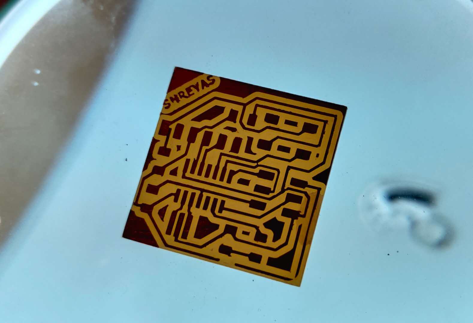
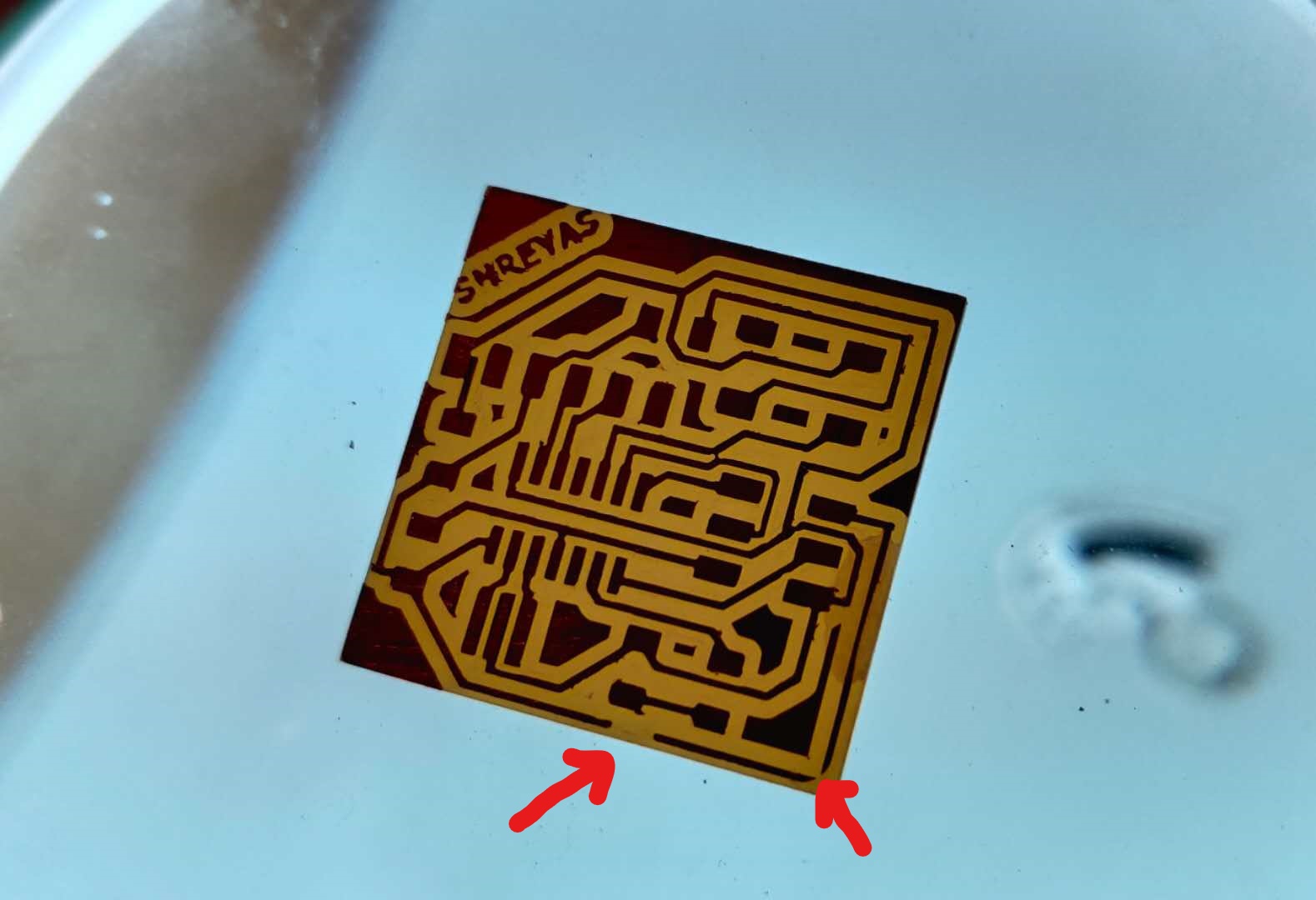
Finally, I exported the image. Before exporting, I hid all the layers, then only selected the Traces and Dimensions Layers to be shown. When exporting, it is important to select monochrome, and to set the resolution at 1000 dpi. When this is exported as PNG image, you can open it in Photoshop to personalize it. I added my name in the corner of the board. I also created the .png file for cutting the board's outline shape. Before saving this, it is important to resize the image to the original size- for some reason, when you export from Eagle, it doubles the size of the drawing. The final outcome looked like this:

Part 3- Milling and Soldering
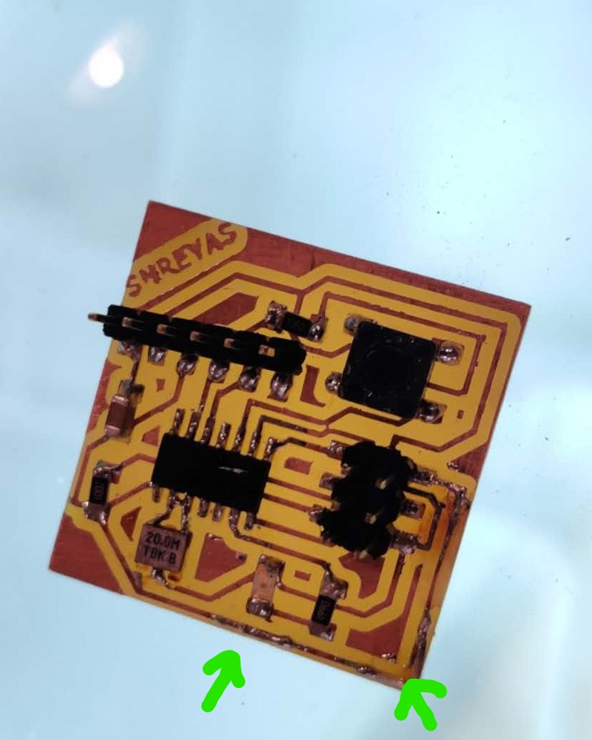
I prepared the .png files using FabModules. I then sent the board to be milled on the Roland SRM-20 machine. To find a detailed explaination of the milling process, click here. I have no errors to report for milling. After the board was traced and cut, I scraped off the copper residue using a metl ruler, then used a magnifying glass and tweezers to remove any small copper fragments that could interfere with the traces. The end result looked like this:
The next step was to collect all the components, then start soldering. When soldering the ATtiny44, I learnt a new soldering technique, where you add a lot of solder on all the legs, then use a hot vaccuum pom to desolder. It worked really well for those components with many solder joints in a small area, such as the FTDI jumper as well. Another thing was that we only had 'through hole' buttons, not SMD versions. So, what we did is bend the legs by 90 degrees, then shorten them to soldered on top of the board. After I had soldered all the components, the final outcome looked like this:
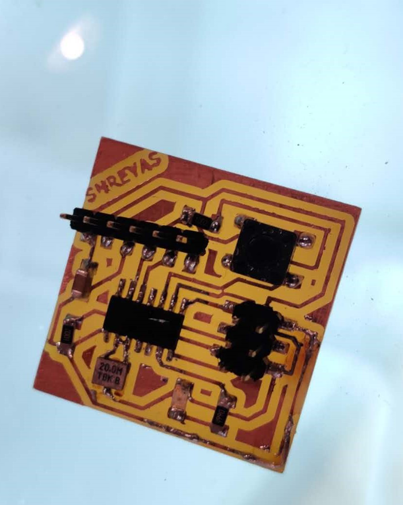
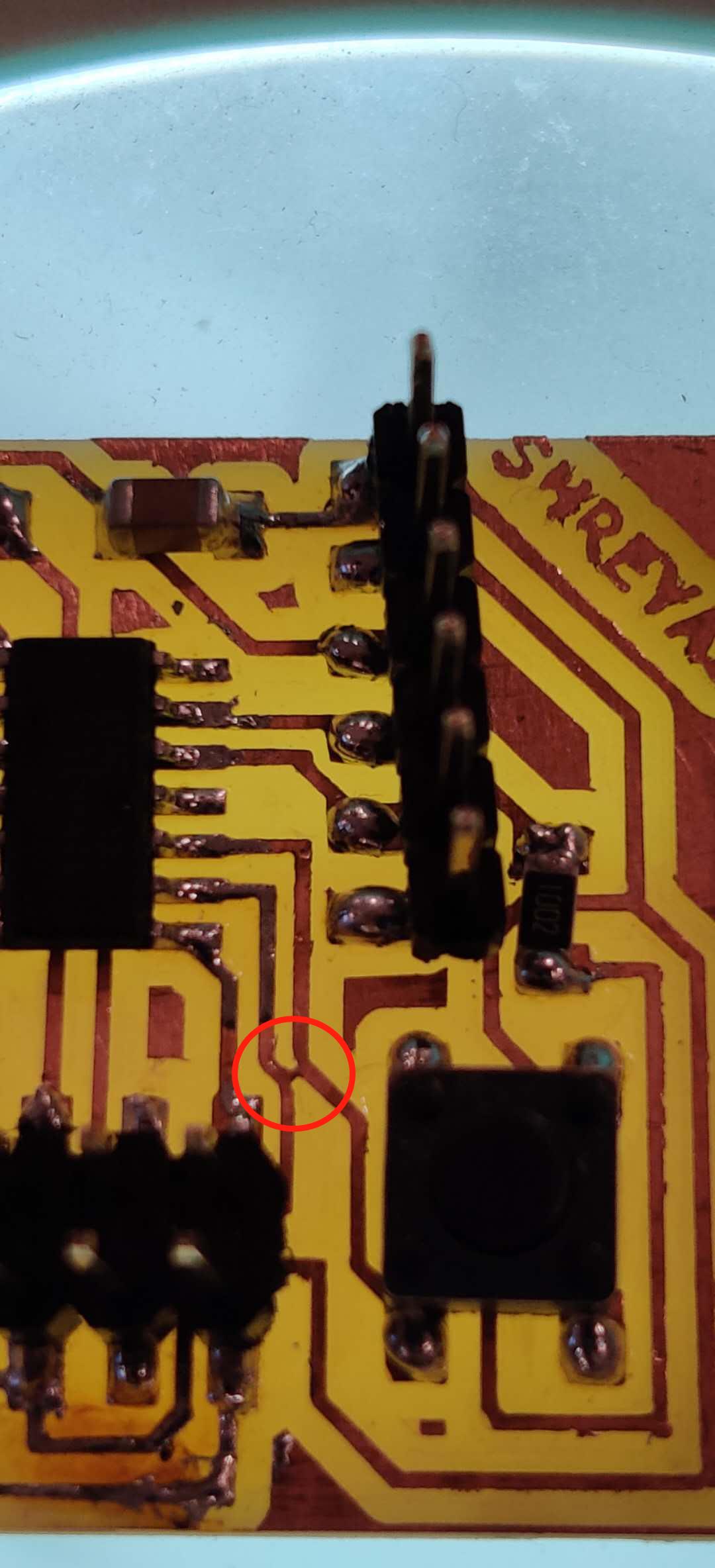
In the image of the milled PCB, you can see that there are 2 areas where the copper trace had been scraped off completely. To fix this, I took an LED, broke its legs, and soldered them directly onto the board.
Part 4- Programming and Testing
I plugged in the FTDI cable to do the smoke test, and right away, I had an error! The LED was lighting up, even though it was not connected to a power source. I examined all the traces, and found a place where two traces were slightly touching. I used a knife to create some distance between them.
I then used a multimeter to check all the traces, where I came across another issue- one of the legs of the ATtiny44 wwere not touching the board. After fixing this, I could continue with the programming of the board. I connected my computer to the FABISP I made 2 weeks ago, which was connected to new board I have made, which was then connected to an external power source.
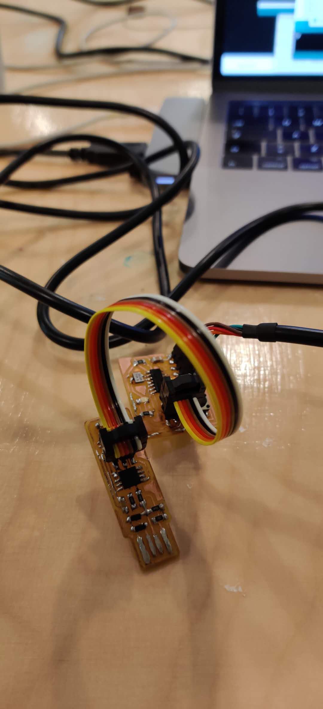
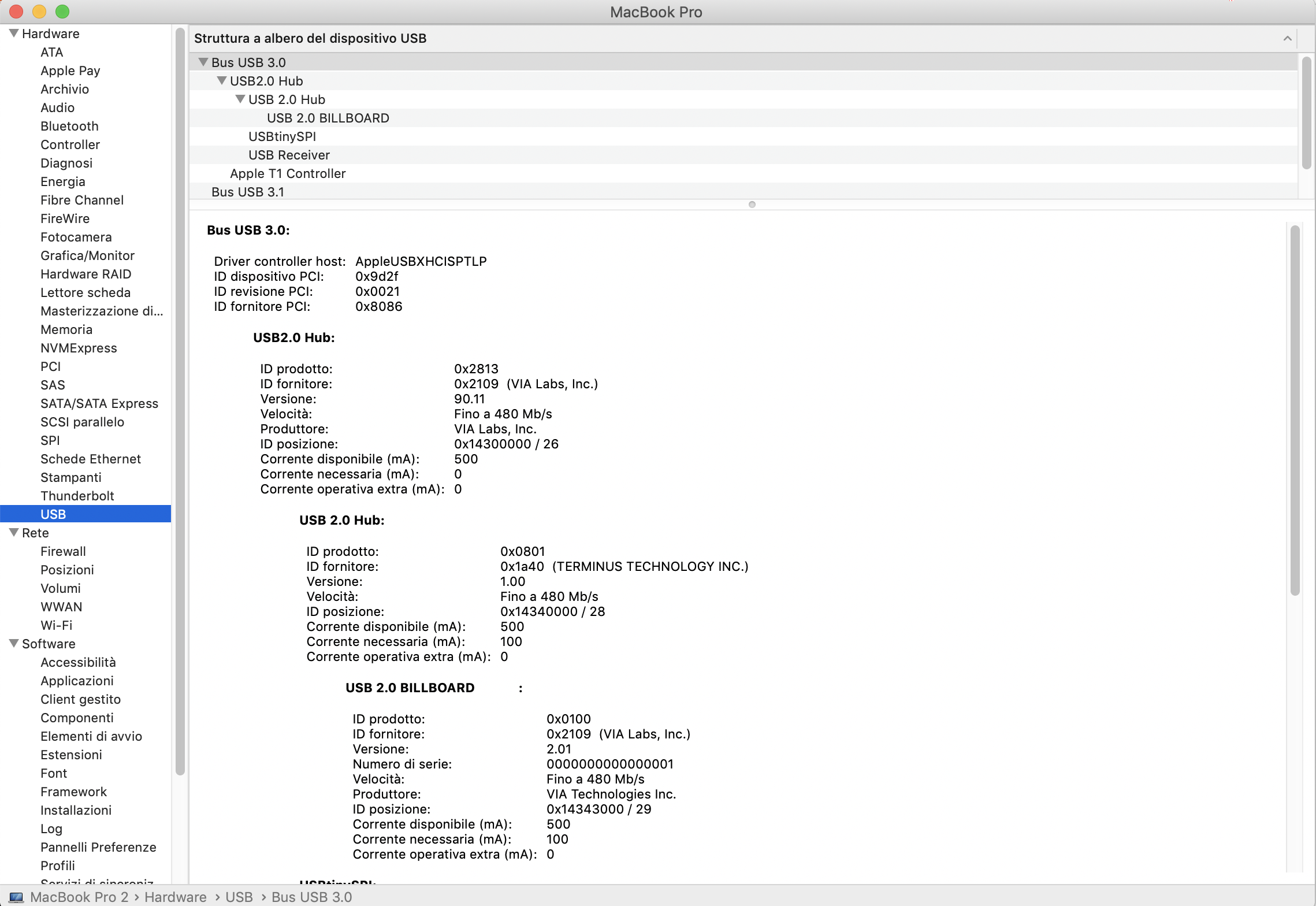
Right away, the computer recognized my board.
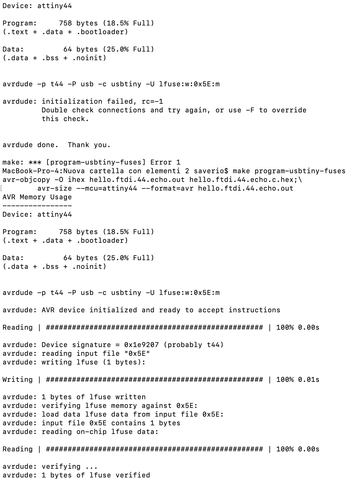
The following commands were run:
- $ make -f hello.ftdi.44.echo.c make
- $ make -f hello.ftdi.44.echo.c make program-usb-tiny-fuses
- $ make -f hello.ftdi.44.echo.c make program-usb-tiny
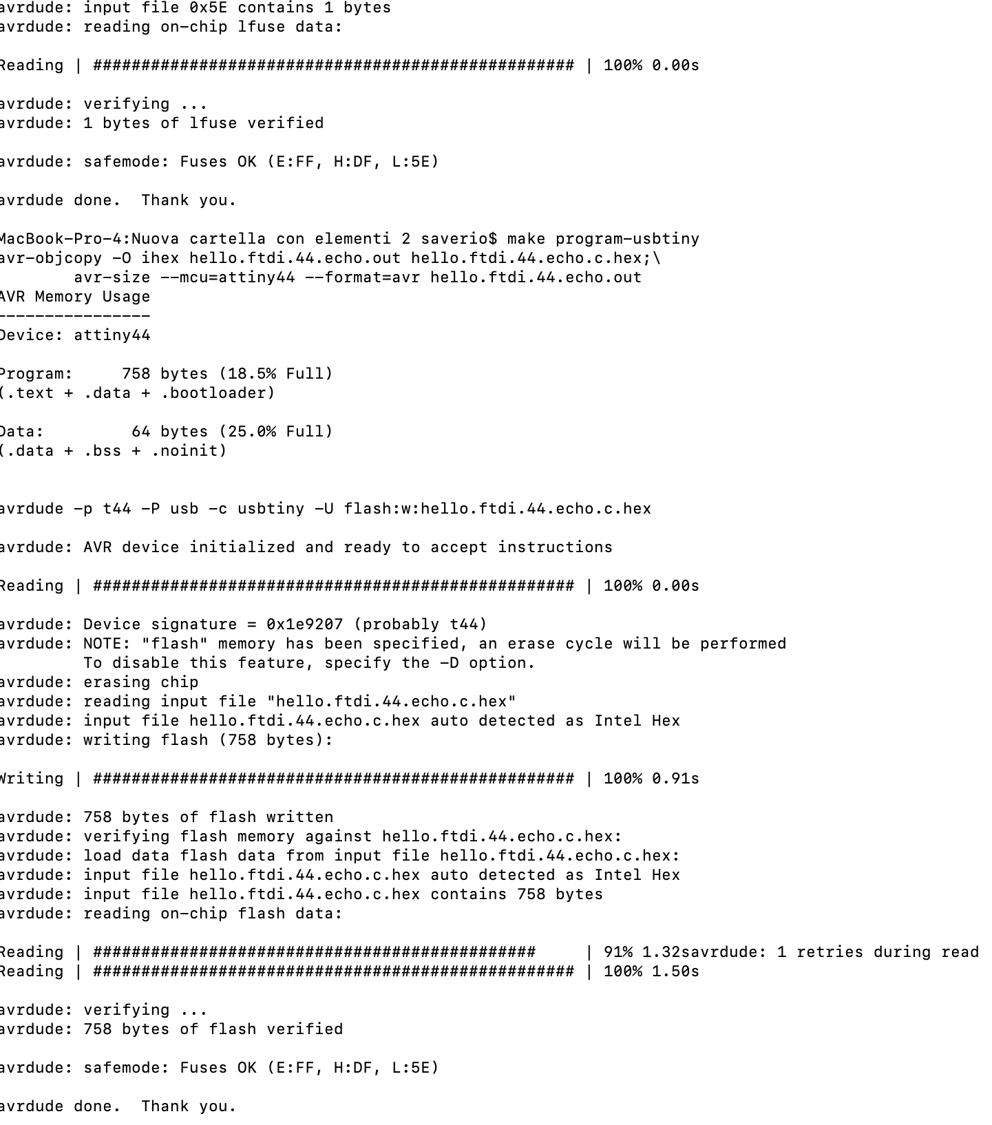
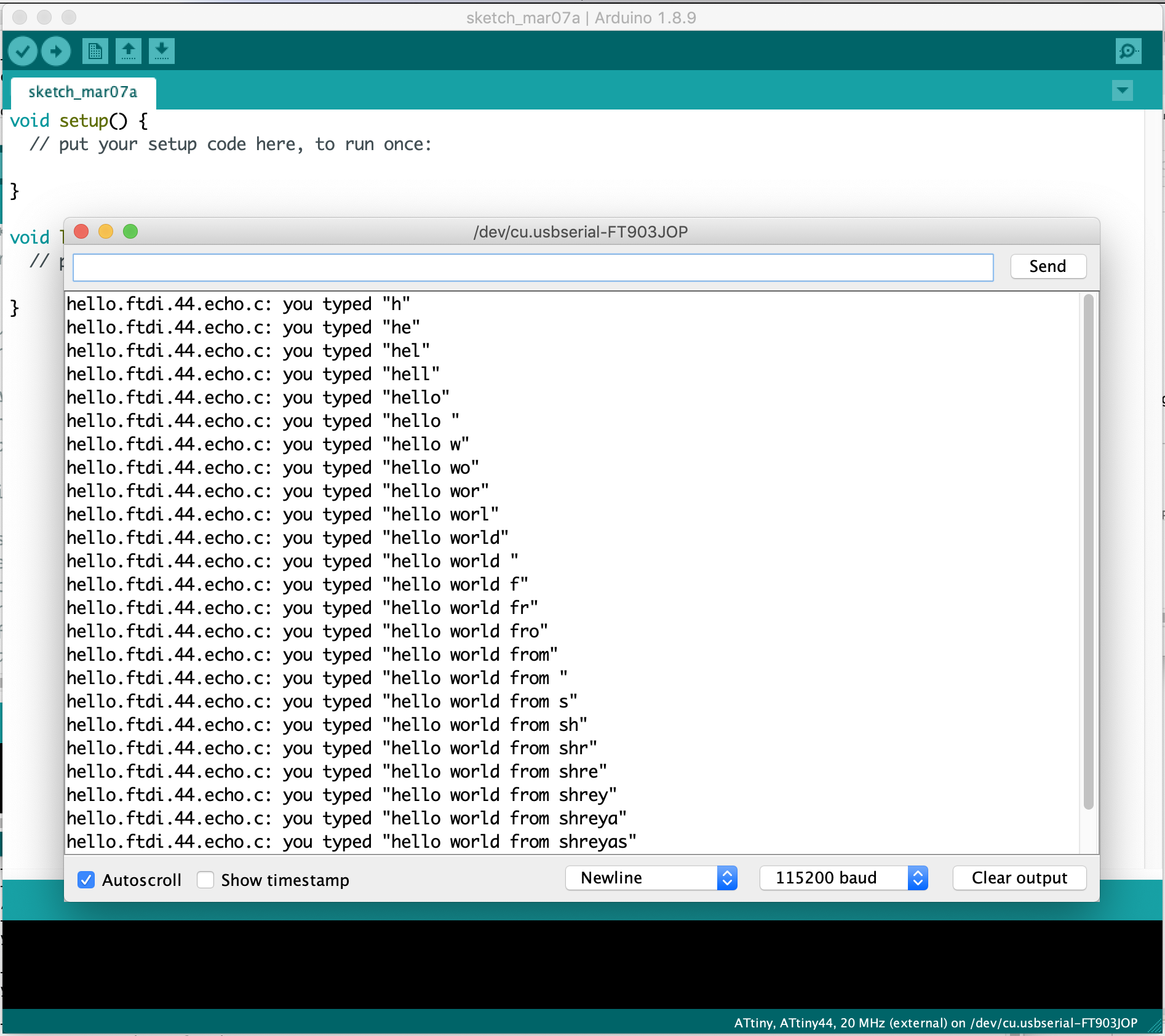
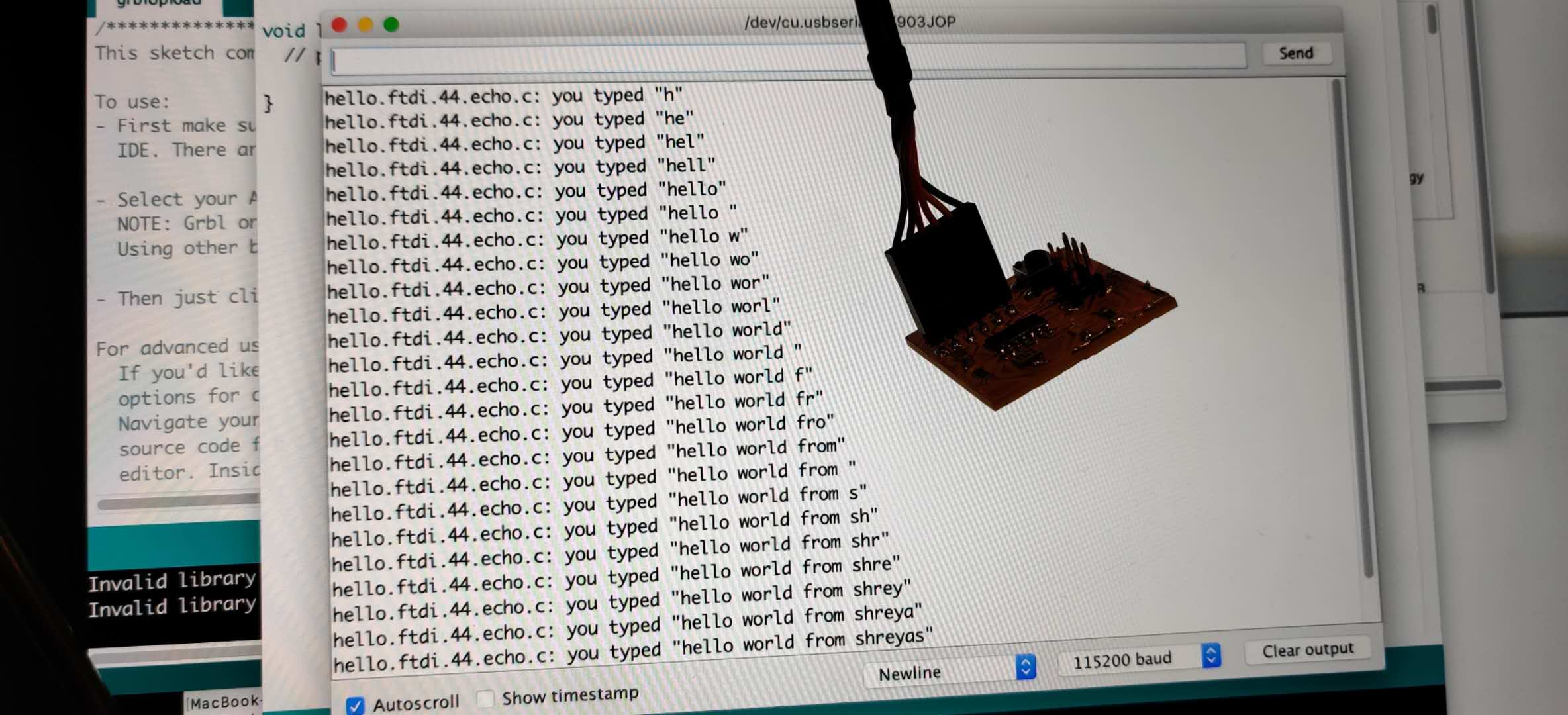
Finally, I opened Arduino IDE, where you need to install the ATtiny package, choose the correct board and Serial Port. The process for installing the ATtiny board in Arduino and setting up the Arduino IDE to communicate with my board (select the board and frequency and the right ftdi port) is documented in the Embedded Programming Page. After this, a window opens, where I successfully tested the echoing function of the assignment.
 Click here to download the Schematic Drawing
 Click here to download the Board Layout Drawing