Electronics Production
Tasks for this week:
- Group- Characterize the Design Rules for the PCB production process.
- Make an In-Circuit Programmer by milling and stuffing the PCB and test it.
Part 1- Group Assignment
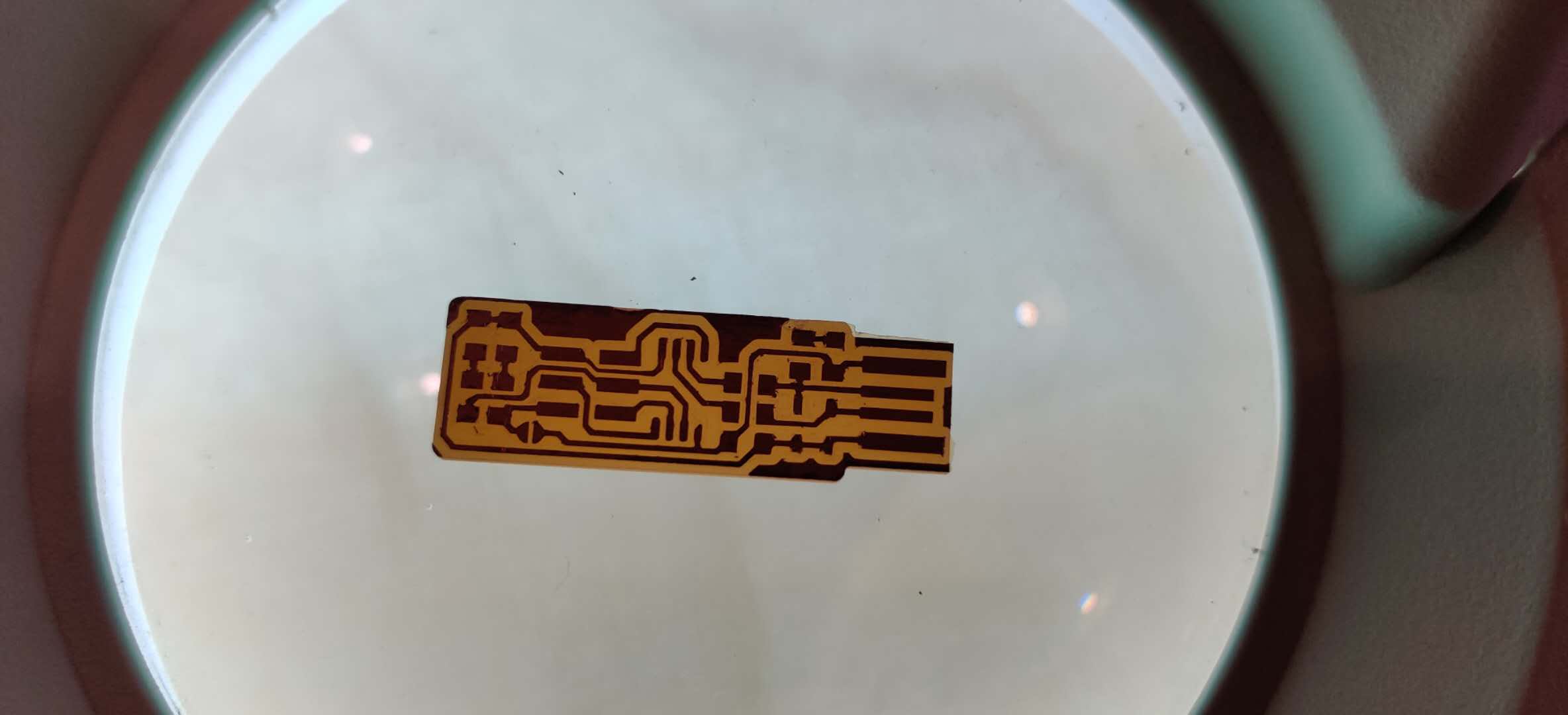
The FabISP is an in-circuit programmer based on the AVR ISP Programmer. For the group assignment, we had to learn the steps of making a PCB. The processes involved included: Sending the traces and outline files to the milling machine using FabModules and setting up the Roland SRM20 milling machine.
We used FabModules to create the .rml extension file for Roland milling machine. All the necessary information to cut the file, such as machine speed, reference for origin, material thickness, tool diameter, offset and more is communicated to the machine. All the details of how to set up the file in FabModules were included in these Instructions.
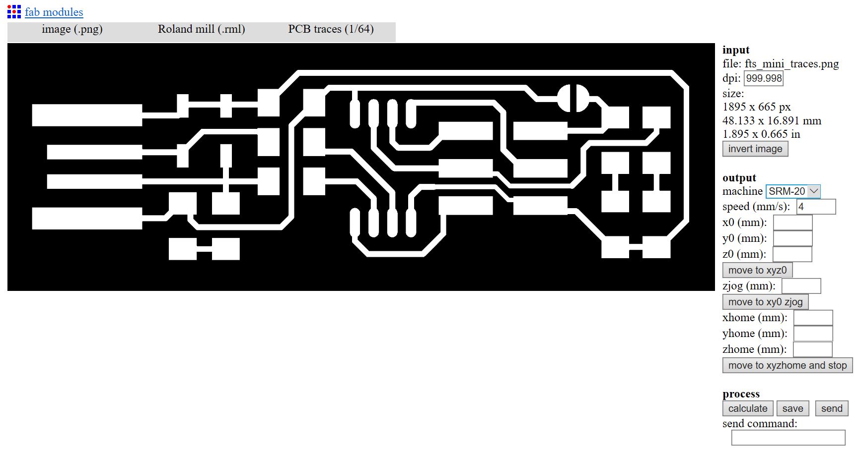
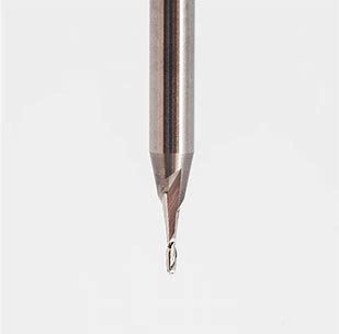
The machine we used for this task is a Roland SRM20, and the material we used for the PCB is a laminate sheet with a very thin layer of copper called FR-1. A very important part of this process was to understand what endmills are appropiate to use for tracing and cutting. In this case we are doing two different tasks, the traces where the machine will remove material without going through will use a 1/64 bit, and the outline cuts require a 1/32 bit.
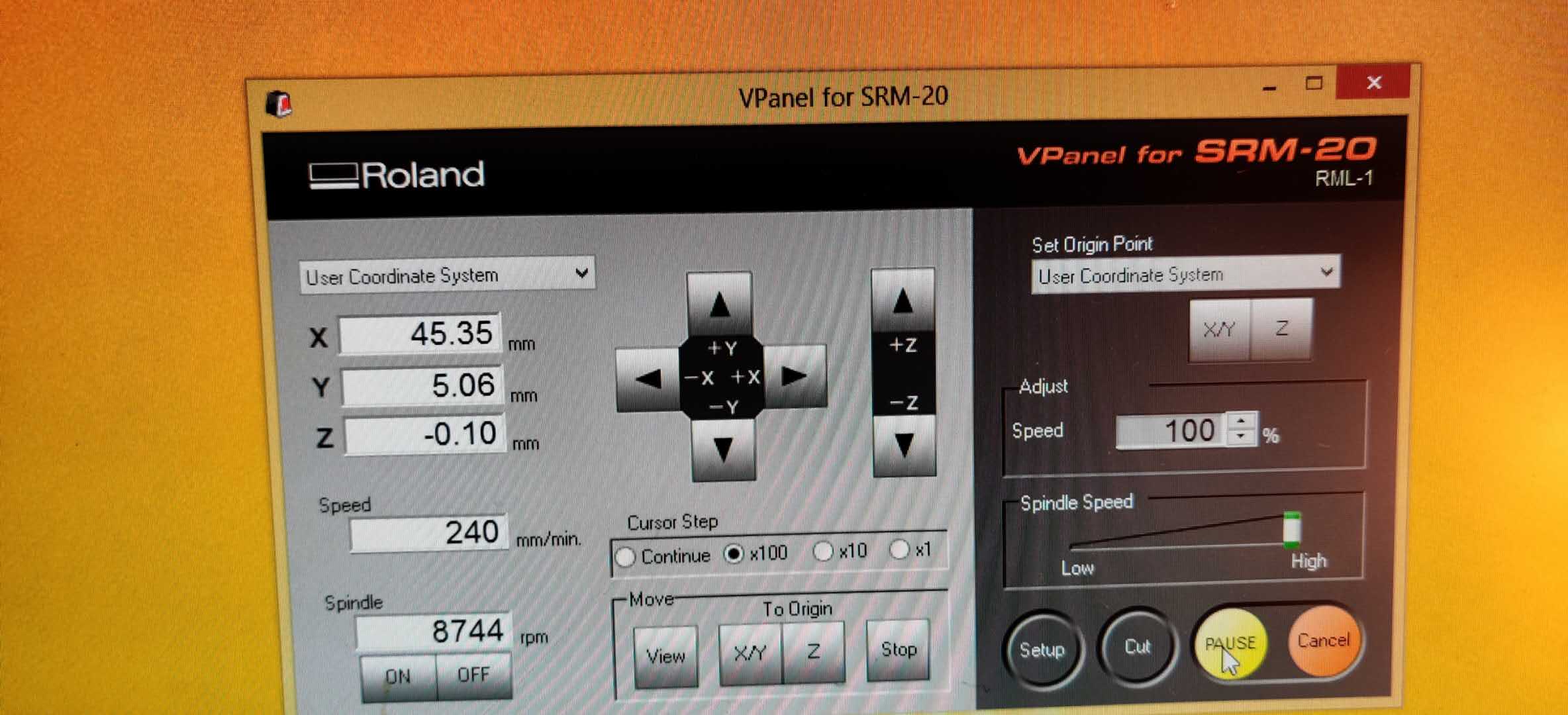
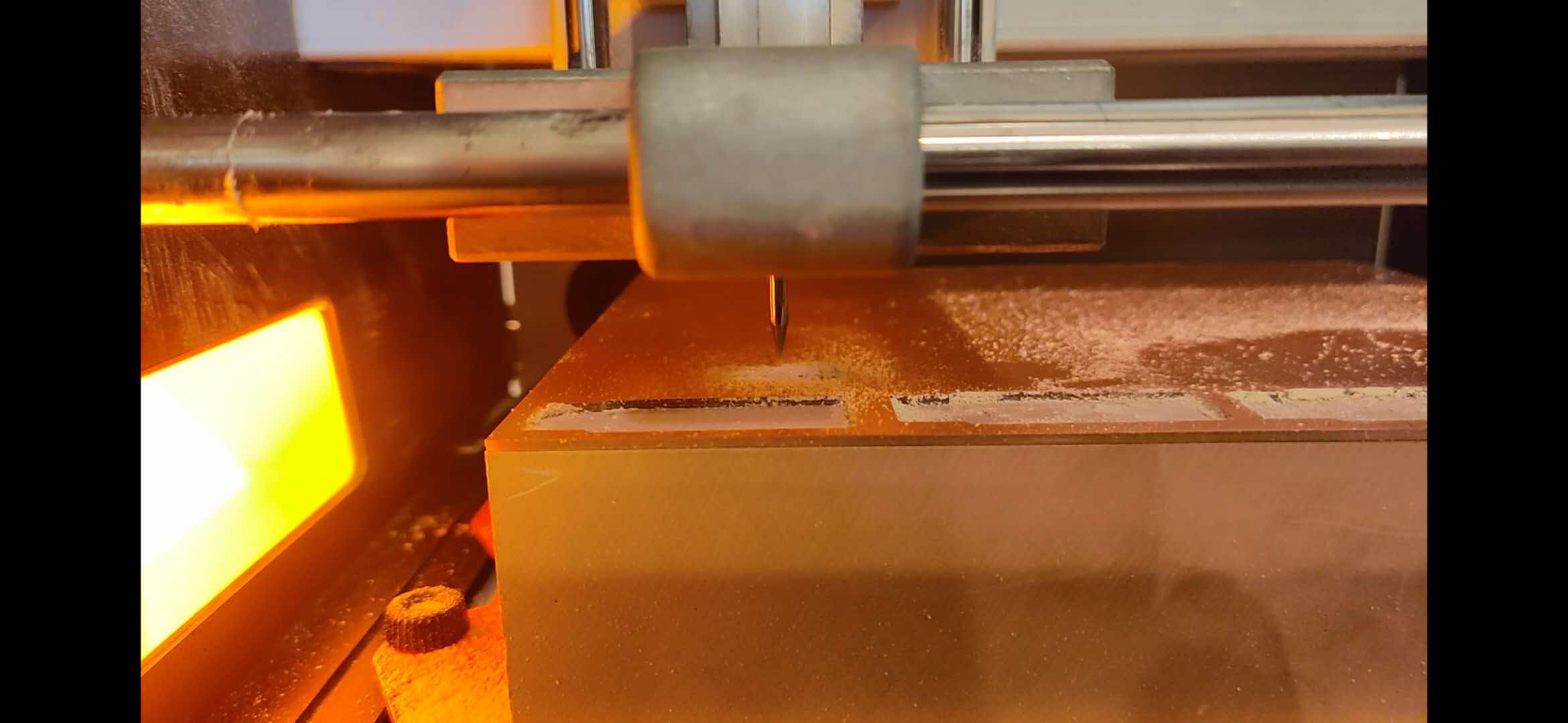
After identifying the appropriate endmill, we learned how to set up the machine's position. We began with the traces task, so we fixed the 1/64 mill bit into the machine. We had to carefully add the bit into the machine, making sure it doesn't fall, which could easily break its tip. The first axis to locate is the Z-axis, where the bit just touches the copper plate. After this, you can set the origin for the Z-axis. After the Z-axis origin point is set, it is important to remember to move the bit UP the Z axis slightly; otherwise, if there is any movement in the X- or Y-axis, the bit could scratch the copper plate, or break the bit. Then, using approximation to move the bit where the FabISP needs to be made, and the X and Y axis origins will also be set. Then, you upload the file with the machine's software, and you start milling. As the bit starts spinning, it is important to hover the mouse over the 'Pause' button, just in case. This process needs to be repeated with the cutting after the tracing, but we must swap the mill bit to a 1/32 for cutting, and the bits should be removed and replaced carefully, so that it doesn't fall out and damage itself, or damage the FR-1 sheet.
After the PCB is milled, it is important to use a metal edge to scrape any copper residue off, then using tweezers and a magnifying glass to remove the smaller copper residue from the traces, so they don't interfere with the connections. To test if the residue has been removed and does not interfere, a multimeter can be used to test the traces' connections.
Part 2- Soldering
Before FabAcademy, I had some experience with soldering, but the small components and size of the board made it a very difficult job. We were given a BOM (bill of materials), that included all the components list and where they should be soldered. Components include:
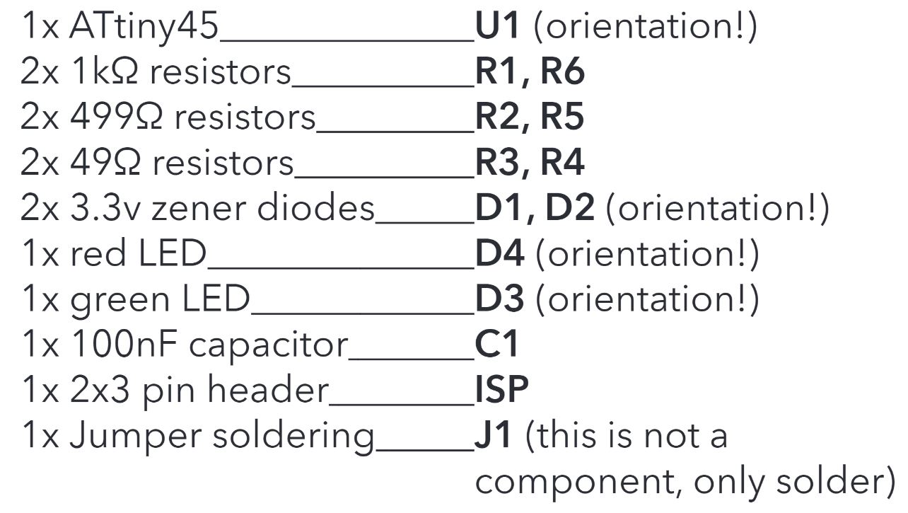
Tip 1: Always begin soldering the middle components and move towards the sides. If you have tall components leave them at the end or else they will block you while you are soldering the other components.
Tip 2: Some components need to be soldered in a certain orientation. Generally, there is a dot that helps understand the correct orientation.
Error! - When soldering the ATtiny 45, which requires soldering in 8 places, I accidentally soldered two of the legs together. Because we were working in a different lab (due to the quarantine closing our actual lab), I could not get a solder sucker or any other device to remove the excess solder. Eventually, after many attempts, I managed to seperate the solders by heating the solder and quickly dividing it when melted with a small, thin piece of plywood. When the solder became solid again, the joint was seperated. For final checks, ensure that the board is cleaned well with alcohol, check all componenets using the multimeter and make sure that there are no short circuits. Also check that the soldering went through the components "legs". It has to flow btween the pin and the copper pad, and no other components are interfering with the solder in a place.
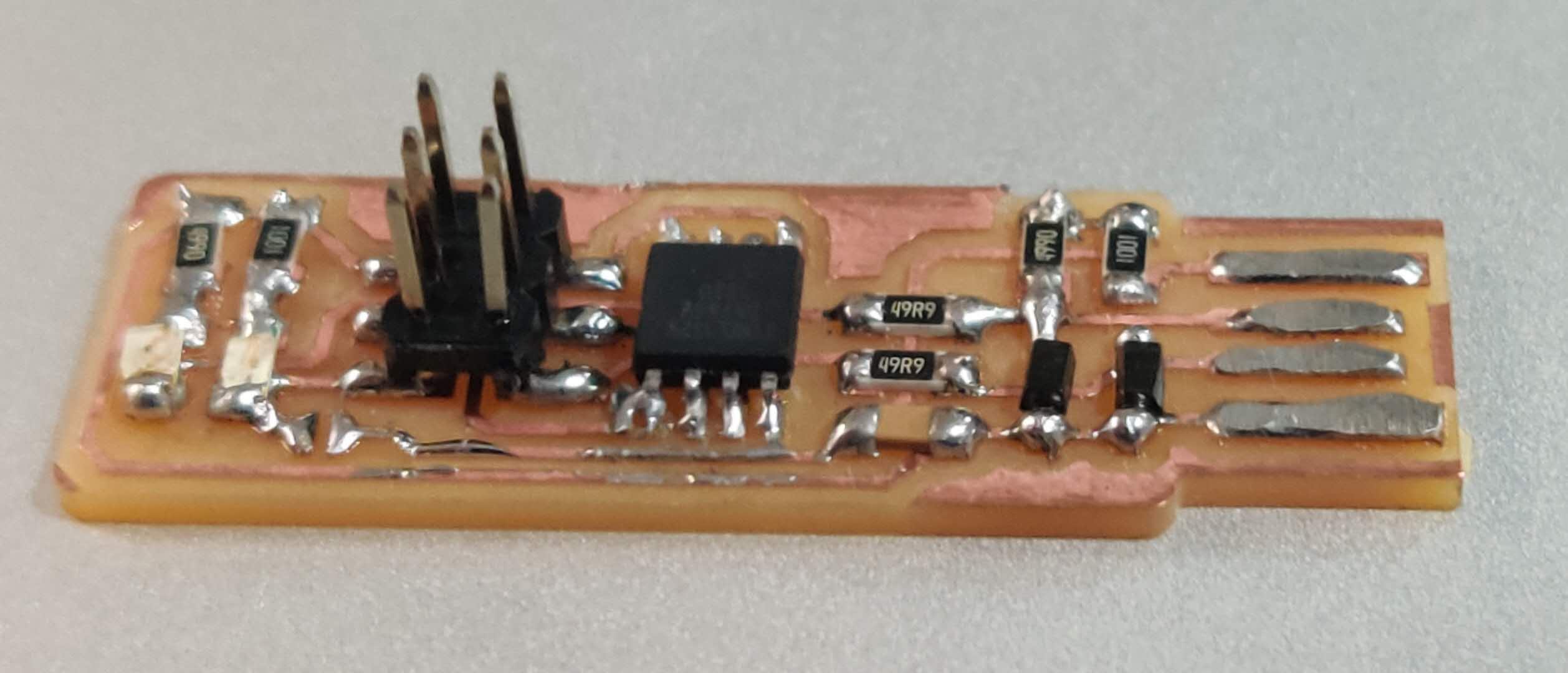
The final outcome looked like this:
Part 3- Testing
Solder was used to create a bridge on the jumper near the ISP header. This temporarily allows the ISP header to be used for programming the ATtiny45. (The programmee supplies voltage on this pin and the programmer detects it). Once it's programmed, the bridge is removed to turn the board into the programmer itself. An ISP cable was used to connect my board to an existing programmer FabISP. The following commands were used to program it:
- make (a file named fts_firmware.hex is created in the folder)
- make flash
- make fuses
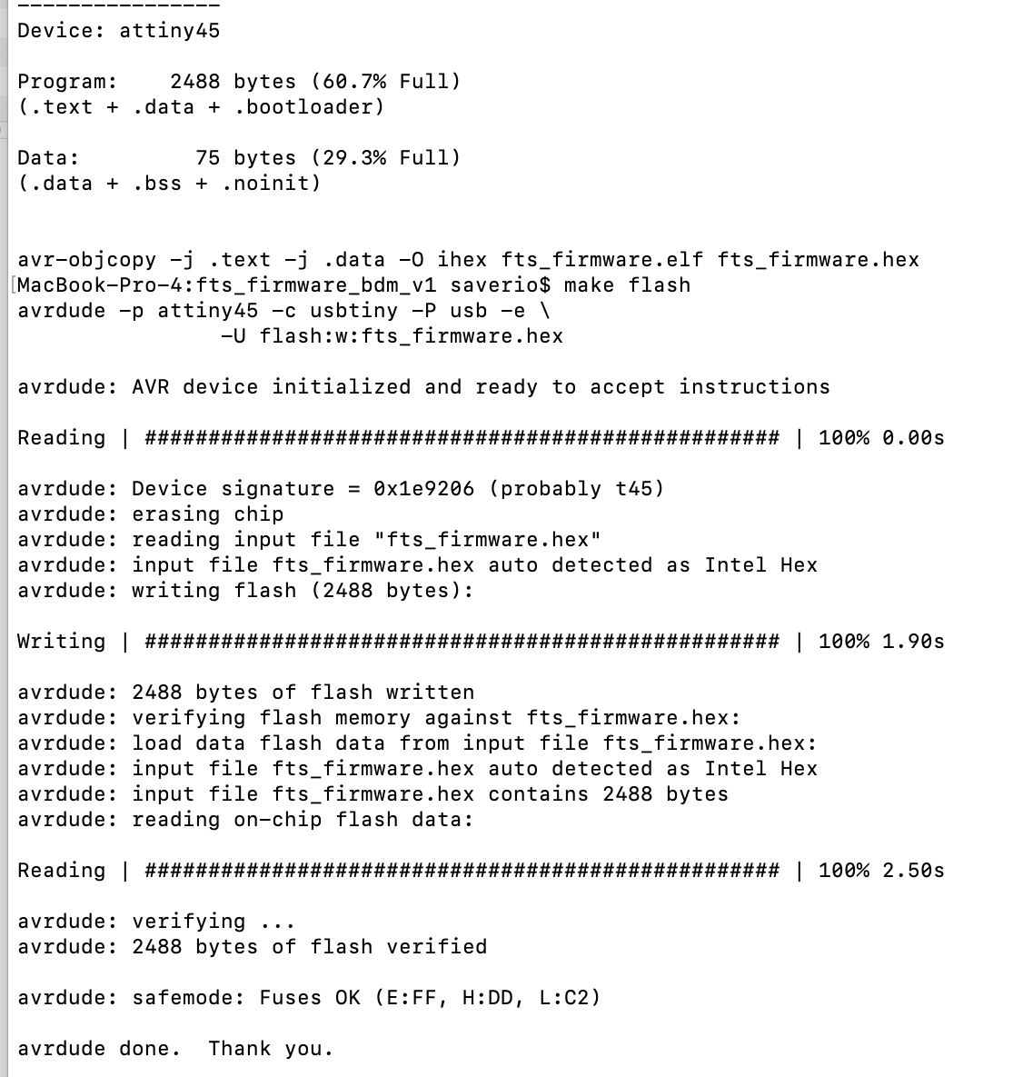
My FabISP succesfully worked when programming it in the first try, and I had to do no troubleshooting whatsoever!!
This was unusual, but I don't have any errors to document 😄
After this, I desoldered the jumper connection, and now I have a working programmer ready to use in future assignments.
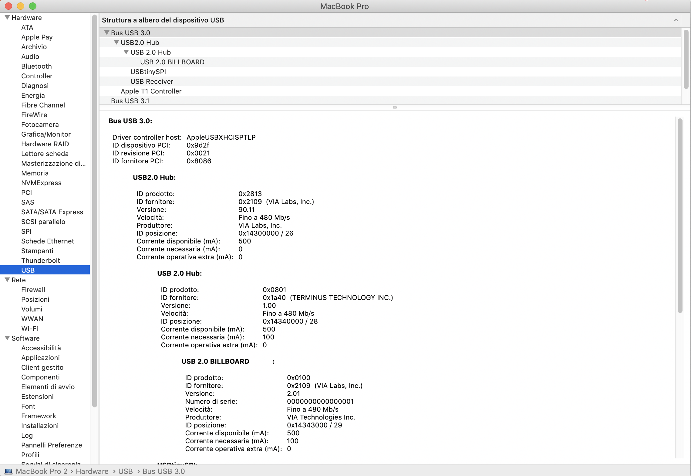
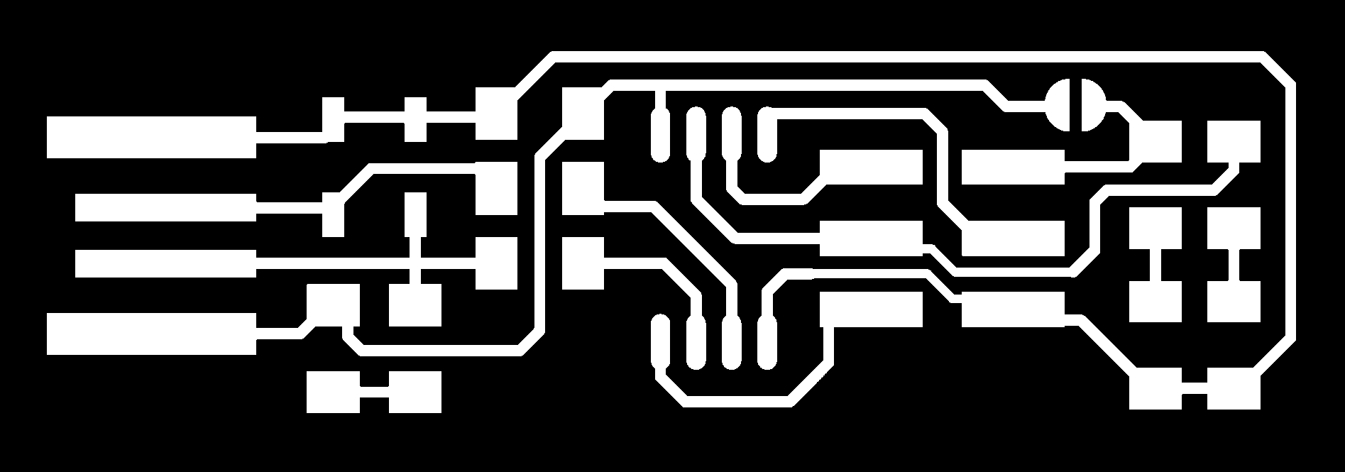
The above picture is a Mac recognizing my FabISP, and I had to use another laptop since my laptop's port was not working. Click here to download the FabISP's Trace
Click here to download the FabISP's Outline