5. Electronic Production
- Characterize the design rules
My group assignment actually is also my individual assignment, as our lab has only me as Fab 2020 student :) Anyway let me get started
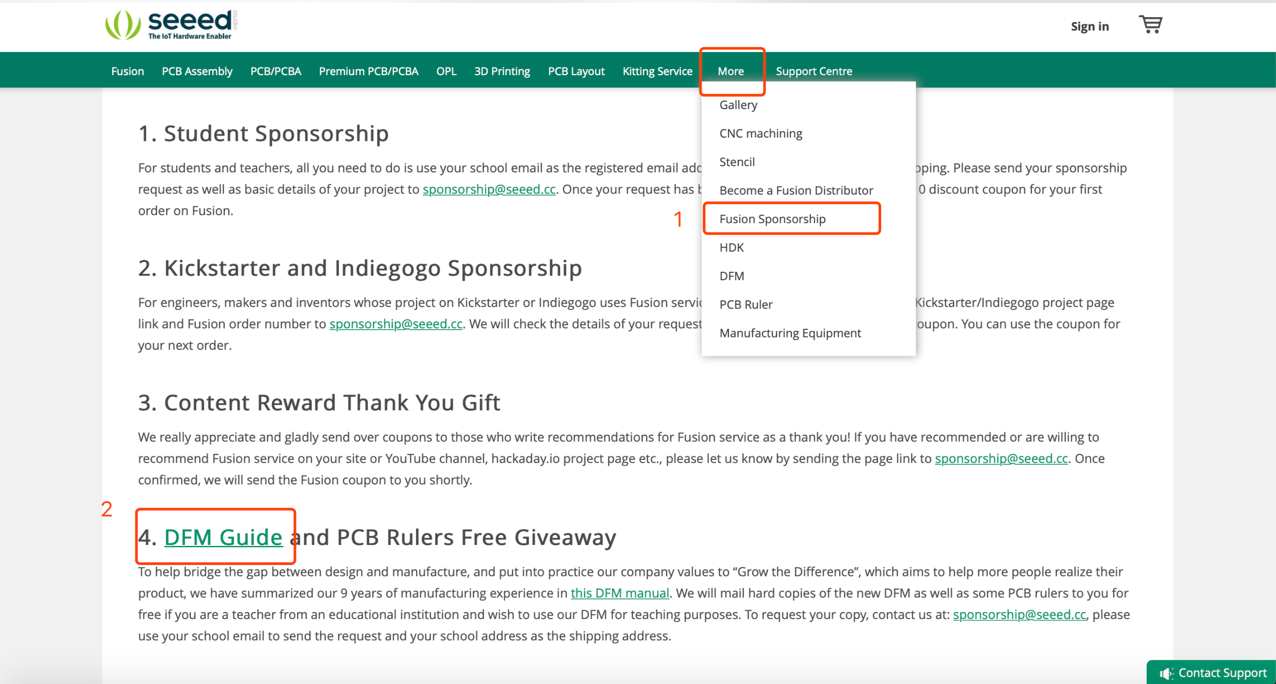
Luckily it is not too difficult for me to understand roughly about a PCB production process, as i'm working at Seeed(which Neil also introduced as a board house. Well not exactly accurate definition of the entire business but we do have this business unit). We have an 43 pages DFM handbook, online(Also hardcopy available) available, also translated to different languages other than English, Japanese, French, German, Russian, Portuguese, etc.

Find the SeeedFusion_DFM here.
The usual way we do mass production of PCB, not using milling machines but etching machines. The process looks like following(in short) -
Design files ready -> Check the design -> Film -> film on FR4(inner layer) -> etching -> Film strip -> inspection -> PP & other layers(outter layers) -> repeat from Film step to strip step -> drilling -> plating -> Inspection.
However from Fab Academy i'm not following the above process, as i'm doing only several boards instead of mass production. I'm using a milling machine instead.
I was using a made-in-China milling machine "JINGYAN". It reads G code. The CAM software also comes with the machine "CopperCAM".
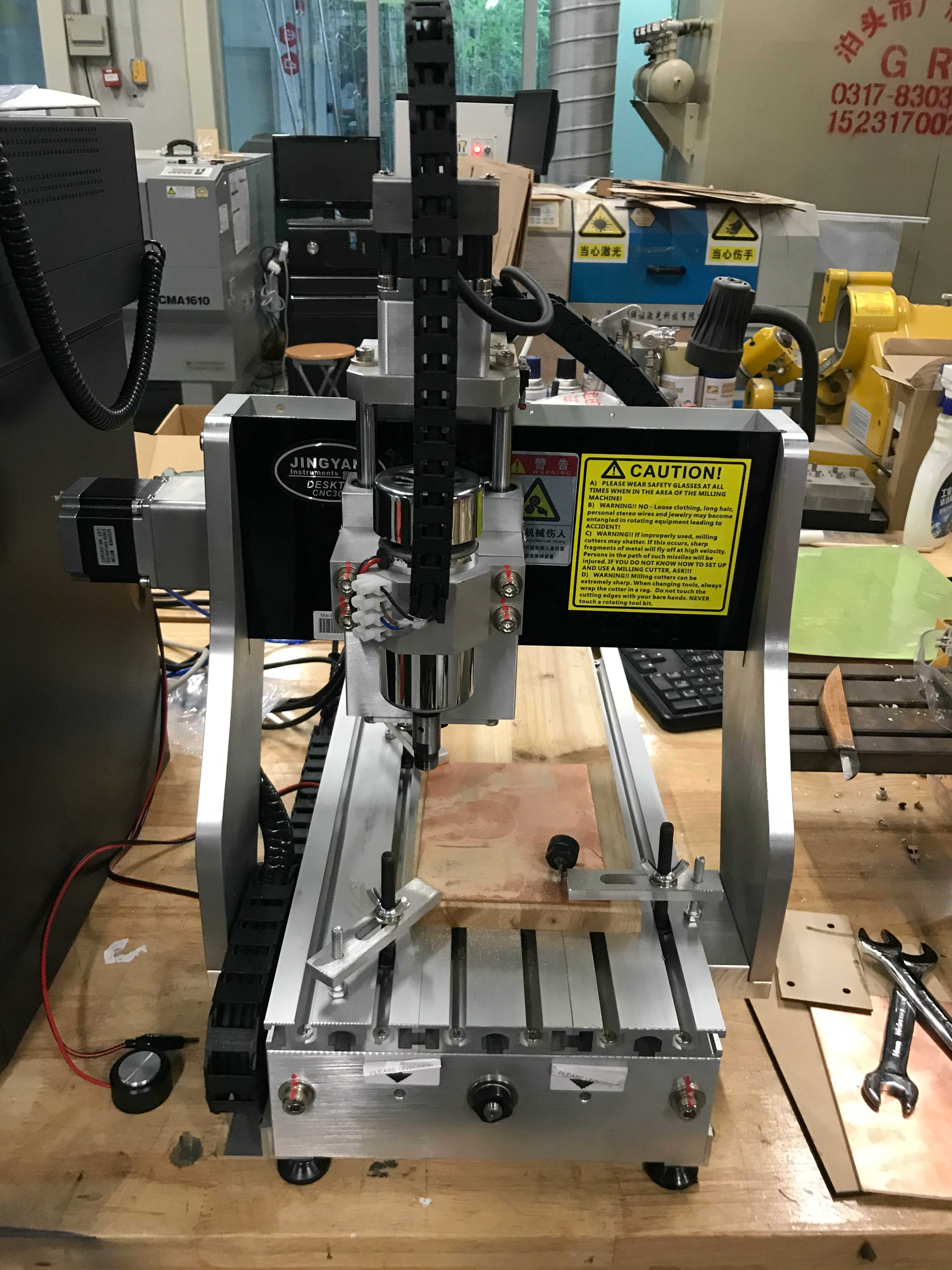
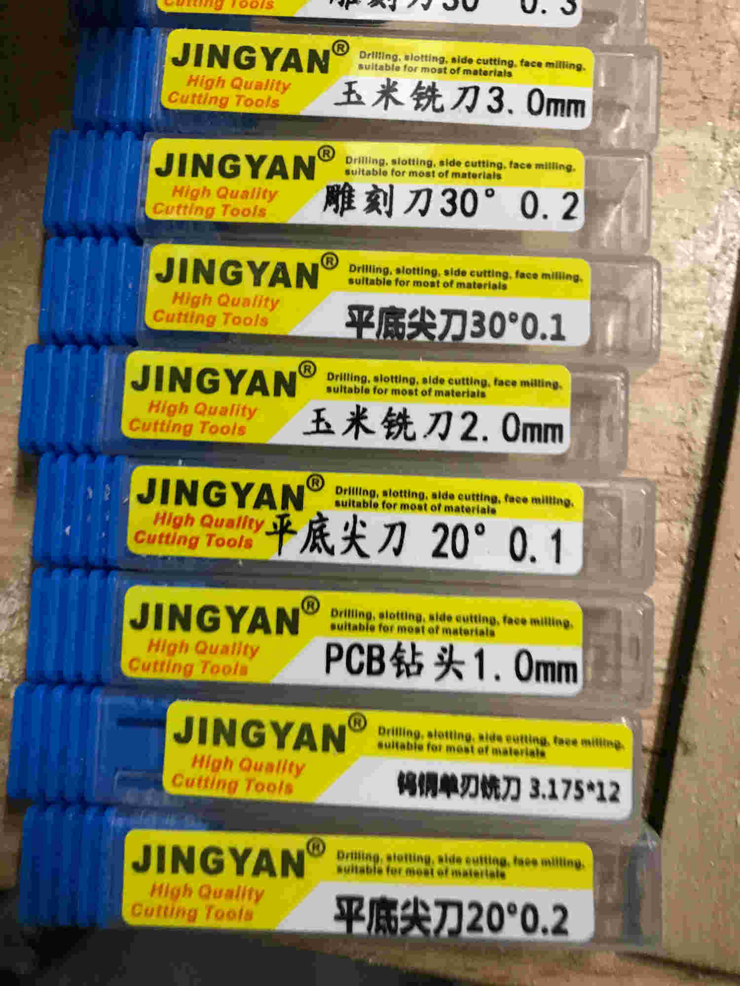
The tools that in the lab we had
Thickness of the copper board : 1.6mm, which means the maximum cutting depth should be no more than 1.6mm - below are the parameters set to the Mods.
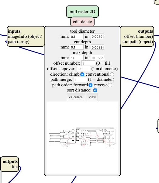
The design rules will be: having a design file ready, go to CopperCAM, and generate Gcodes. Then adjusting the milling machine, by making the Copper board stays flat, Selecting the machining tools, checking the focus, zeroing the tool, everything ready and start milling the different layers with changing tools in the between.