Embedded Programming (WEEK 9)
Individual Assignment:
- Compare the performance and development workflows for other architectures
Group Assignment:
- Read a microcontroller data sheet program your board to do something, with as many different programming languages and programming environments as possible
IMPORTANT NOTE : ALL OF MY IMAGES ARE POP UP IMAGES , IF YOU HAVE ANY PROBLEM READINGS THOSE IMAGES , PLEASE CLICK ON THEM AND THEY WILL ENLARGE AUTOMATICALLY AND YOU CAN READ THEM EASILY
Embedded System
An embedded system is a dedicated computer system designed for one or two specific functions. This system is embedded as a part of a complete device system that includes hardware, such as electrical and mechanical components. The embedded system is unlike the general-purpose computer, which is engineered to manage a wide range of processing tasks.
Microprocessor VS Microcontrollers
Microprocessor is a central processing unit (CPU) on a single chip. but in Microcontrollers it consist of CPU,Memmory Unit (RAM , ROM )and I/O's . but Microcontrollers is extremely slow when comparing Microprocessor
First before we can move on to programming of our board there are some steps which are required to be perform
SOFTWARE USED
Arduino
Arduino is an open-source hardware and software company, project and user community that designs and manufactures single-board microcontrollers and microcontroller kits for building digital devices. Its products
are licensed under the GNU Lesser General Public License (LGPL) or the GNU General Public License (GPL), permitting the manufacture of Arduino boards and software distribution by anyone. Arduino boards are available
commercially in preassembled form or as do-it-yourself (DIY) kits.
Arduino board designs use a variety of microprocessors and controllers. The boards are equipped with sets of digital and analog input/output (I/O) pins that may be interfaced to various expansion boards ('shields')
or breadboards (For prototyping) and other circuits. The boards feature serial communications interfaces, including Universal Serial Bus (USB) on some models, which are also used for loading programs from personal
computers. The microcontrollers can be programmed using C and C++ programming languages. In addition to using traditional compiler toolchains, the Arduino project provides an integrated development environment
(IDE) based on the Processing language project.
YOU CAN DOWNLOAD ARDUINO OPEN SOURCE SOFTWARE THROUGH THIS LINK
Microcrontroller used
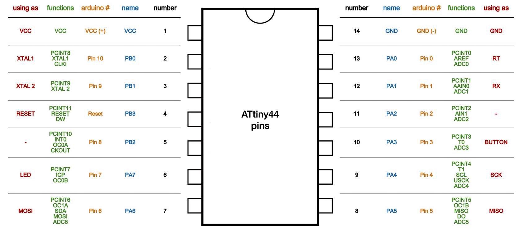
1. Attiny 44
ATtiny (also known as TinyAVR) are a subfamily of the popular 8-bit AVR microcontrollers, which typically has fewer features, fewer I/O pins, and less memory than other AVR series chips. The first members of this family were released in 1999 by Atmel (later acquired by Microchip Technology in 2016). ATtiny microcontrollers specifically exclude various common features, such as USB peripheral, DMA controller, a crypto engine, or an external memory bus.
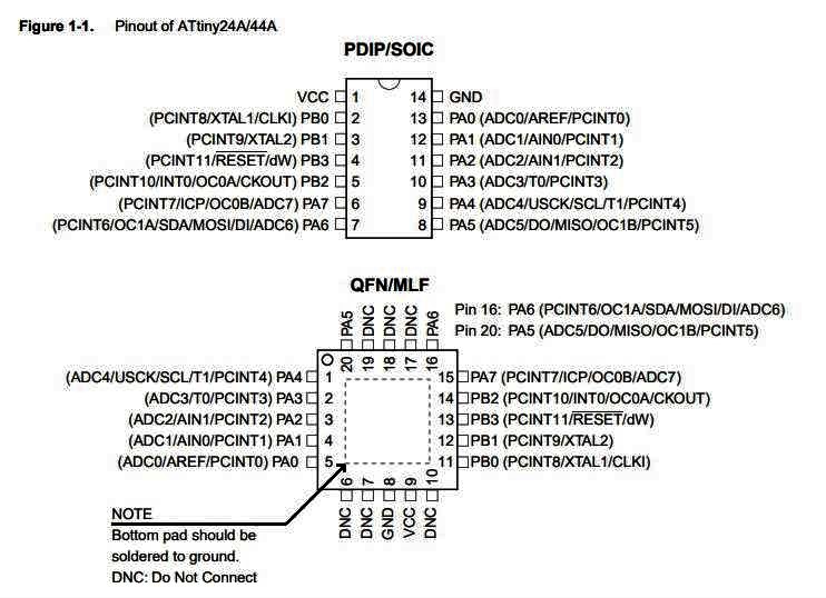
1.1 Pin Descriptions
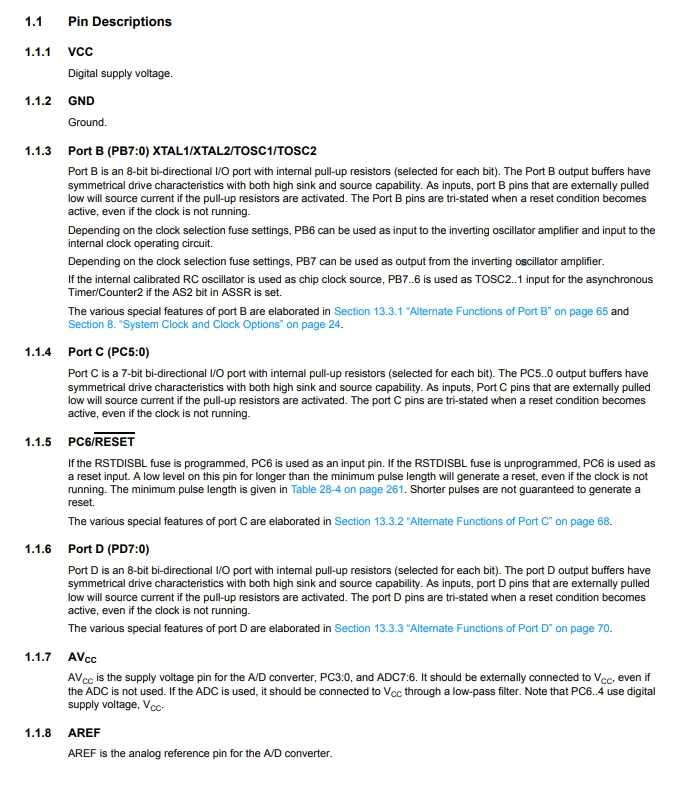
1.1.1 VCC
Supply voltage. 1.1.2 GND Ground.
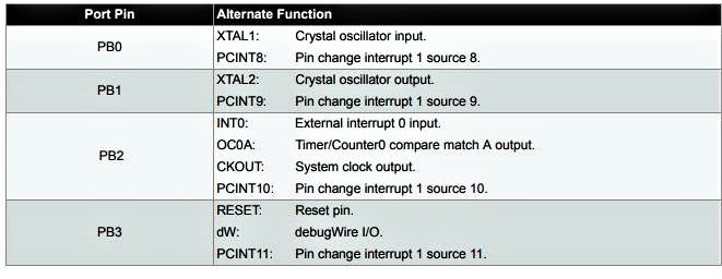
.1.3 Port B (PB3...PB0)
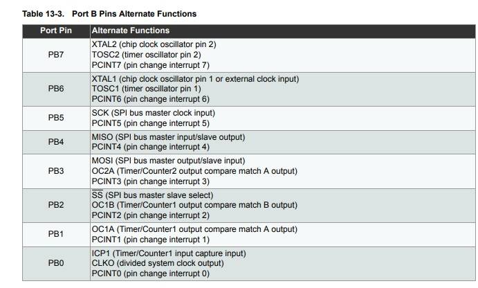
Port B is a 4-bit bi-directional I/O port with internal pull-up resistors (selected for each bit). The Port B output buffers have symmetrical drive characteristics with both high sink and source capability except PB3 which has the RESET capability. To use pin PB3 as an I/O pin, instead of RESET pin, program (‘0’) RSTDISBL fuse. As inputs, Port B pins that are externally pulled low will source current if the pull-up resistors are activated. The Port B pins are tri-stated when a reset condition becomes active, even if the clock is not running. Port B also serves the functions of various special features of the ATtiny24A/44A as listed in
1.1.4 RESET
Reset input. A low level on this pin for longer than the minimum pulse length will generate a reset, even if the clock is not running and provided the reset pin has not been disabled. The minimum pulse length is given in Table 20-4 on page 176. Shorter pulses are not guaranteed to generate a reset. The reset pin can also be used as a (weak) I/O pin
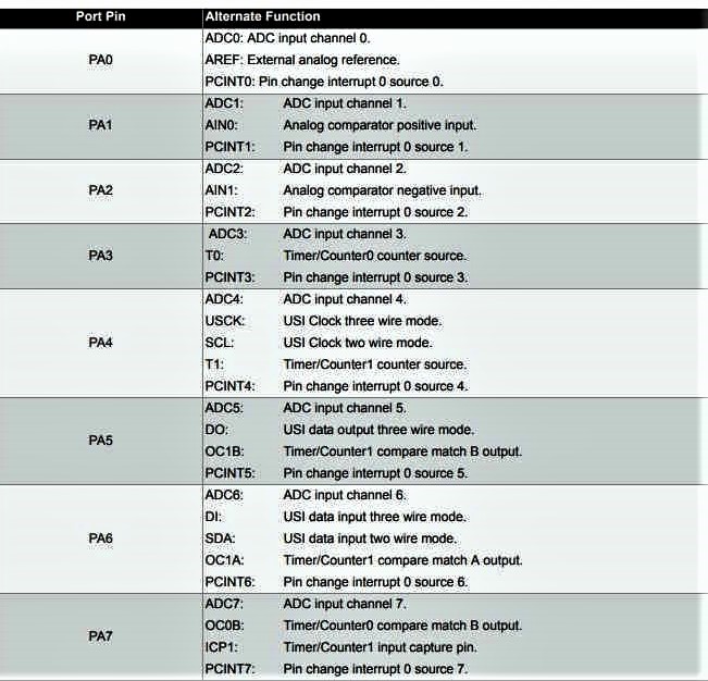
1.1.5 Port A (PA7...PA0)
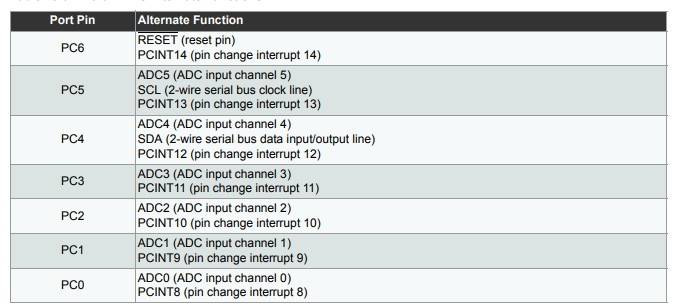
Port A is a 8-bit bi-directional I/O port with internal pull-up resistors (selected for each bit). The Port A output buffers have symmetrical drive characteristics with both high sink and source capability. As inputs, Port A pins that are externally pulled low will source current if the pull-up resistors are activated. The Port A pins are tri-stated when a reset condition becomes active, even if the clock is not running. Port A has alternate functions as analog inputs for the ADC, analog comparator, timer/counter, SPI and pin change interrupt as described in “Alternate Port Functions”
If you want to know more about this microcontroller pls ckick on the is link
Preparing Arduino Ide for Attiny 44
Well if you have worked with Arduino Ide , you will understand that arduino Ide doesnt have Attiny 44 as a board selection and if you didnt worked on it , please be free to check by clicking on TOOLS >> BOARDS
so we require to add some libraries so it can works with attiny 44 as well
The link for Attint 44 library is
https://raw.githubusercontent.com/damellis/attiny/ide-1.6.x-boards-manager/package_damellis_attiny_index.json
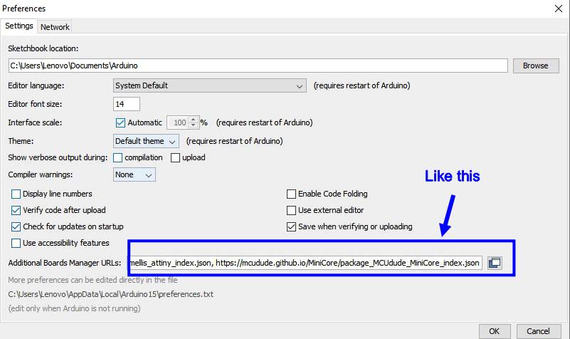
copy this link and paste in the preferences and then follow the this tutorial
Pls go through this video tutorial which i specially made to show how you can add those libraries and
Overview
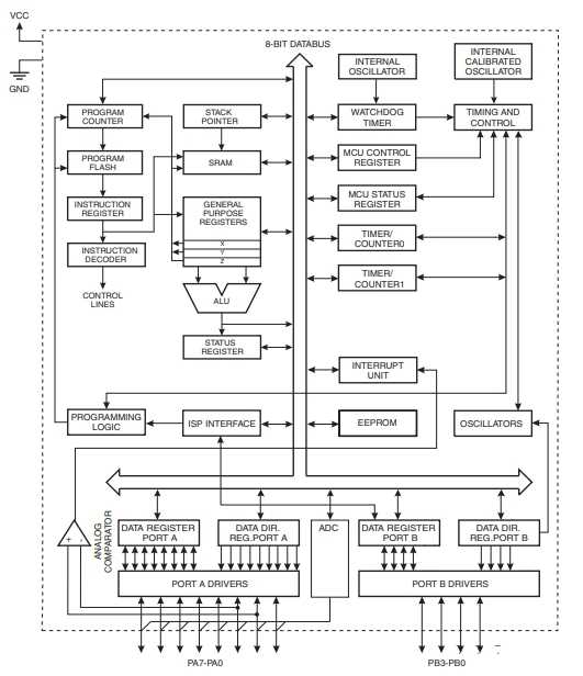
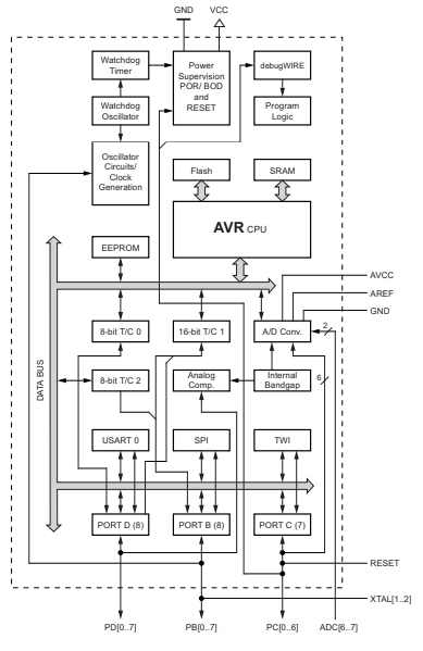
ATtiny24A/44A are low-power CMOS 8-bit microcontrollers based on the AVR enhanced RISC architecture. By executing powerful instructions in a single clock cycle, the ATtiny24A/44A achieves throughputs approaching 1 MIPS per MHz allowing the system designer to optimize power consumption versus processing speed.
>Program Memory Type      : Flash
>Program Memory           : 4KB
>CPU Speed                : 20 MIPS
>RAM Bytes                : 256
>DATA EEPROM Bytes        : 256
>Digital Communication    : 1SPI , 1 I2C
>Capture/ Compare / PWM Peripherals : 1 Input Capture, 1CCP, 4 PWM
>Timers                   : 1 x 8bit, 1 x 16bit
>Comparators              : 1
>Temperature Range        : -40 to 85
>Operating Voltage        : 1.8 to 5.5V
>Pin Count                : 14
2. Atmega 328p
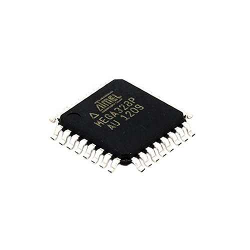
Overview
The Atmel® ATmega328P is a low-power CMOS 8-bit microcontroller based on the AVR® enhanced RISC architecture. By executing powerful instructions in a single clock cycle, the ATmega328P achieves throughputs approaching 1MIPS per MHz allowing the system designer to optimize power consumption versus processing speed
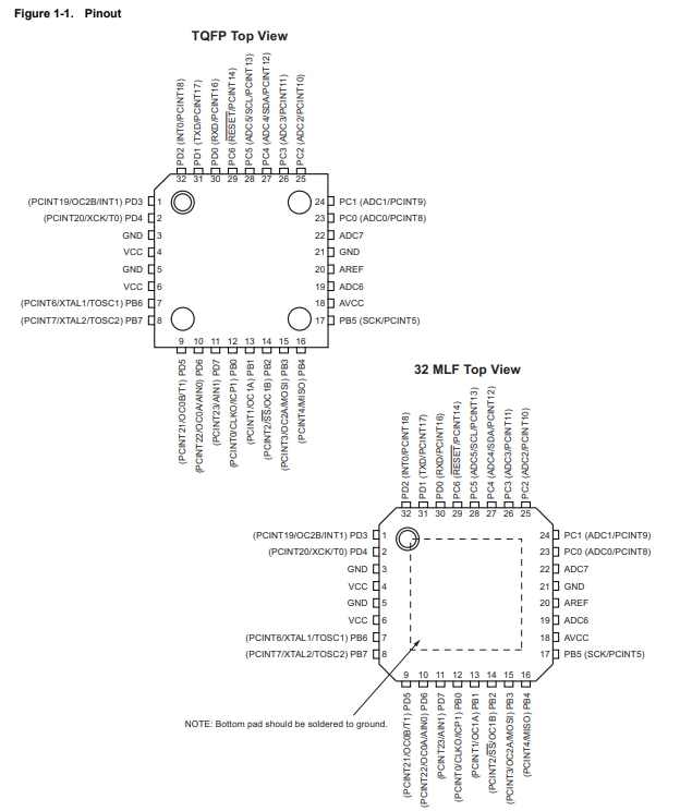
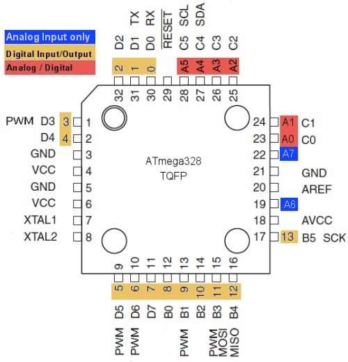
This is the basic pin diagram of ATMEGA 328P SMD(Surface mounted Devices) chipset
Preparing Arduino Ide for Attiny 328p
Similaarly like attiny 44 ARDUINO IDE doesnt recognise the atmega 32p chipset when we tru to program it , besides ArduinoUno is also running on the same chipset i.e. Atmega 328p, but we require to download theboard library for the chipset
Like how we have download the library for Attiny 44 we require to download a library for Atmega 328p, I have given a similar link for what i have provided for Attiny 44 pls paste this link in the bOard preference exactly in same manner
"https://mcudude.github.io/MiniCore/package_MCUdude_MiniCore_index.json"
If you want some more information pls check this datasheet
Programming the board
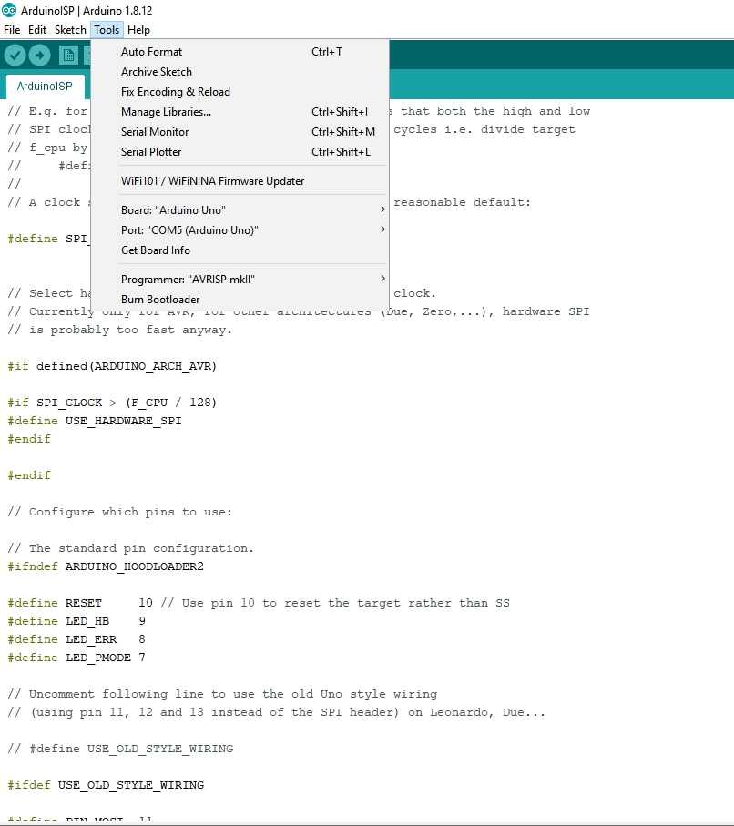
* First open Arduino Ide and then click on FILE >> EXAMPLES >> ArdionoISP and upload the code to arduino
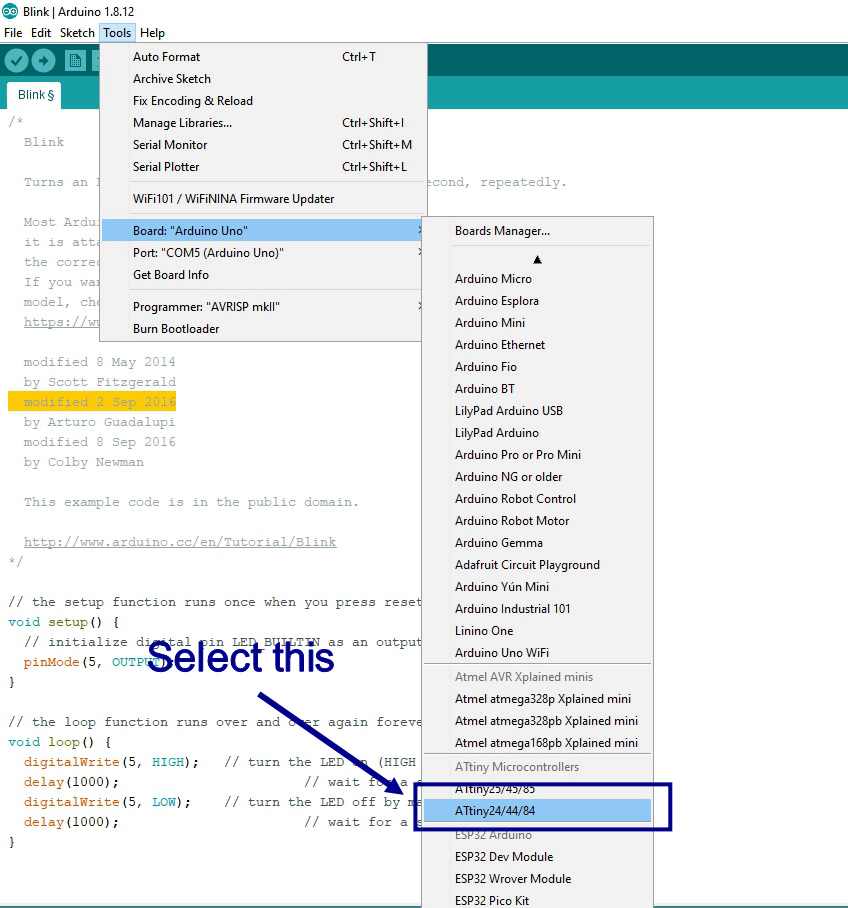
* Then switch the board to ATTINY 44 from the board menu
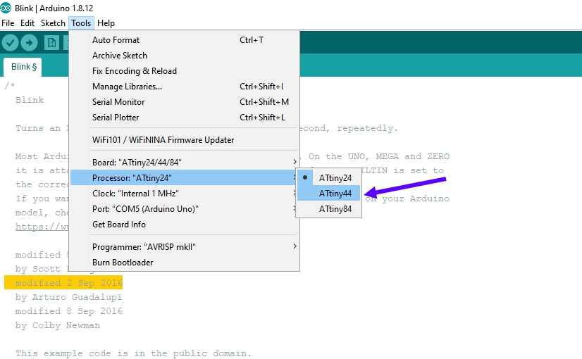
* Then change the procesor to ATTINY 44
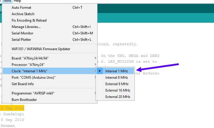
* and change Clock to "INTERNAL 1MHz"
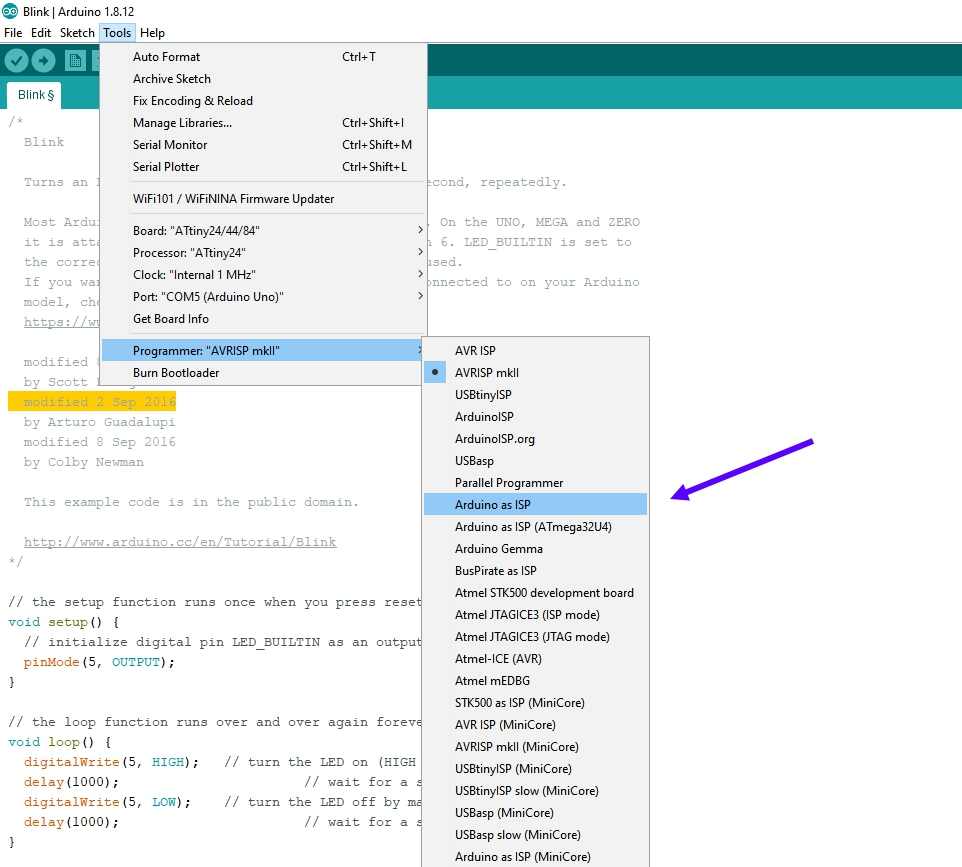
*Then change to programmer to "ARDUINO AS ISP"
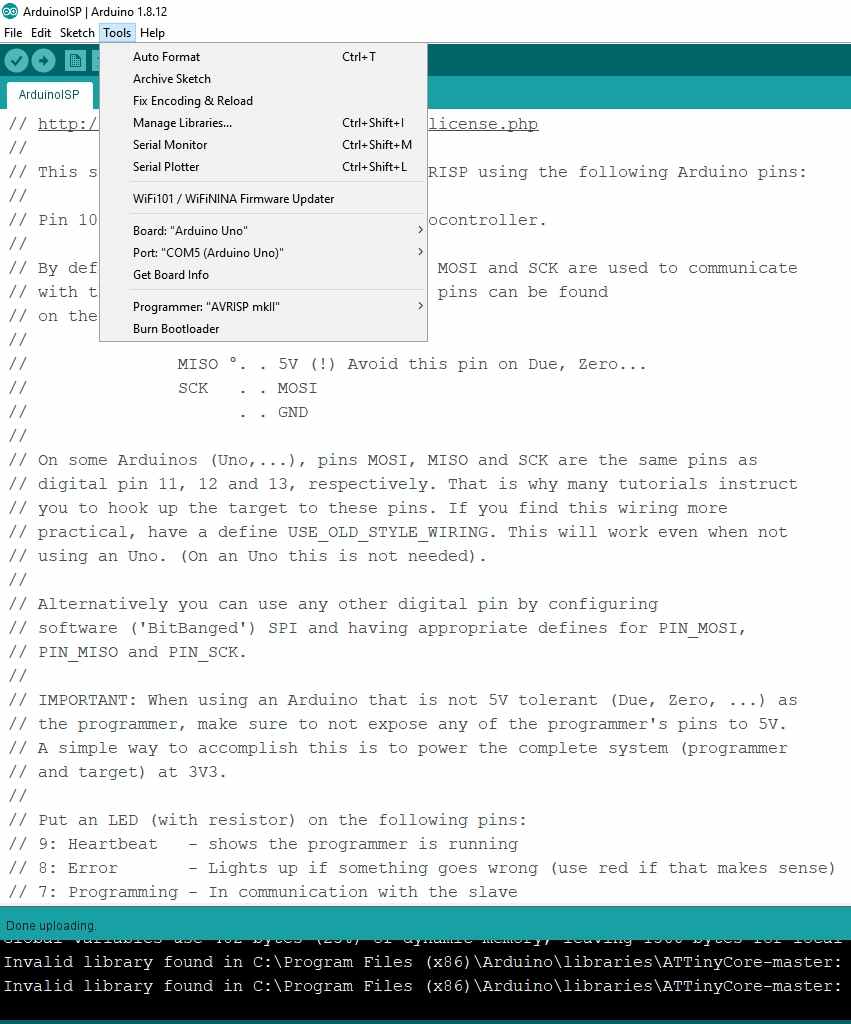
* Then click on the "BURN BOOTLOADER" , so the code for ARDUINOISP can uplaoded to your PCB
Now your pcb is ready to upoad the code
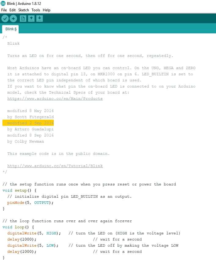
* For testing Upload a blink code by clicking on FILE >> EXAMPLES >> BLINK , as my led was on PIN 5 thats why i edited it to Pin 5 , if you like you can change it
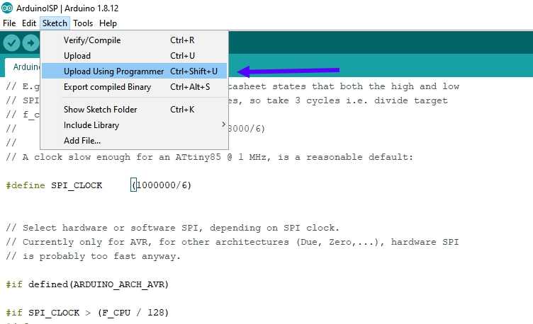
Well remember that there is a little difference while uploading code , i.e you required to upload the code using Arduino programmer o please click on SKETCH >>UPLOAD USING PROGRAMMER
Making connections btw ARDUINO UNO AND YOUR PCB
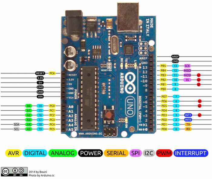
This is the detail schematic of ARDUINO UNO , explaining all the pins uses and nameing them
For our purpose we require only 6 pins
1. GND - GROUND
2. VCC - SUPPLY VOLTAGE
3. PB2 - PIN 10 - RST - RESET
4. PB3 - PIN 11 - MOSI
5. PB4 - PIN 12 - MISO
6. PB5 - PIN 13 - SCK
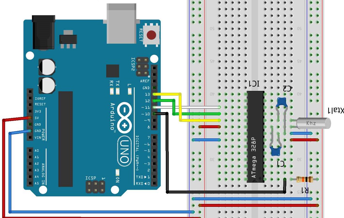
Connection should be made something like this
Programming my board
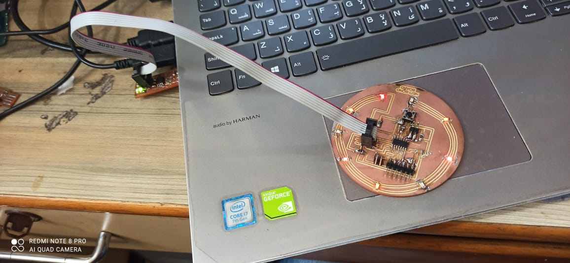
1. NEO ECHO BOARD
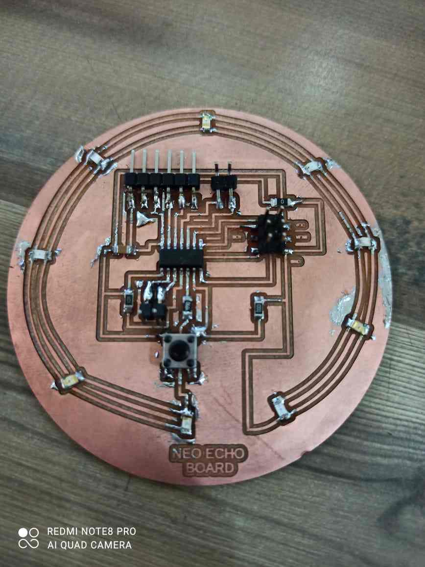
I think you have met my latest creation " Neo echo board , if not pls click on this link to have a look on it
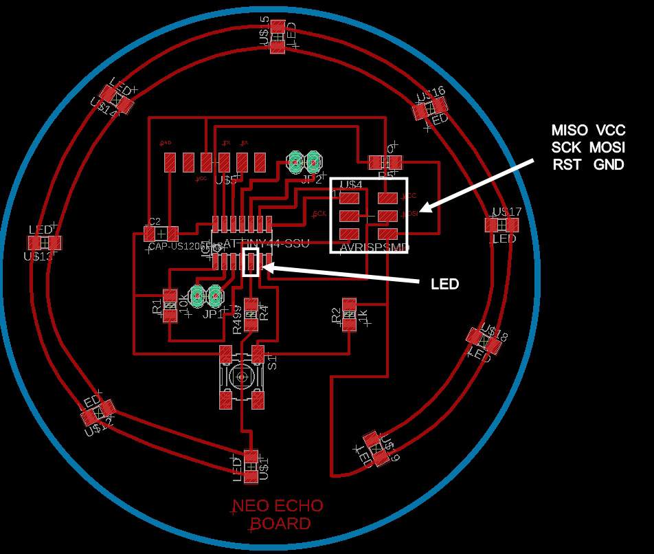
While designing i provided these pins for programming you can have a look to it ,this board is an Attiny 44 microcontroller board
Once you made connections correctly pls follow the above steps where you left for programming , now just required to upload the program only
1. Fab filter Mark 1 ISP
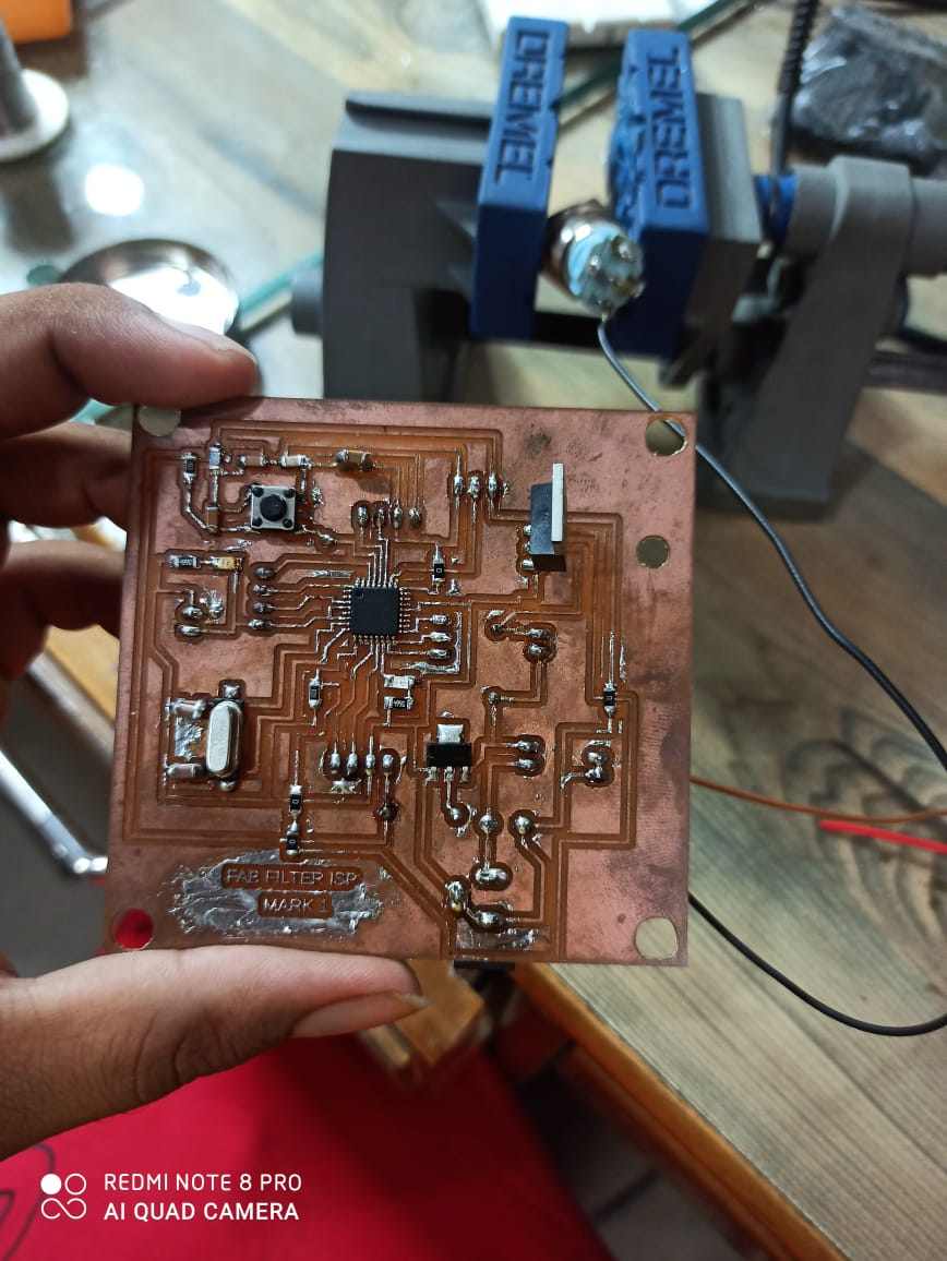
On the contrary to last PCB i have made this pcb for my final project and this is an ATMEGA 328P chipset based PCB so programming it requires a little bit change
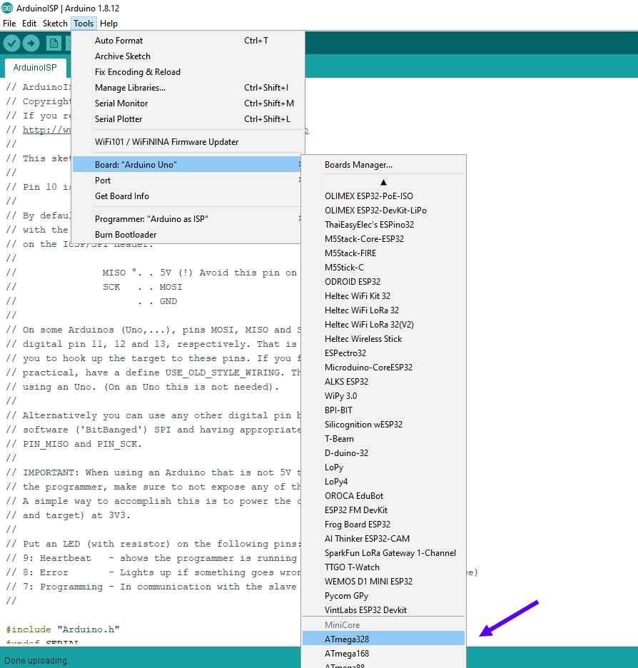
The process is same to the last one , but the difference is that you required to change the board in menu to "Atmega 328p
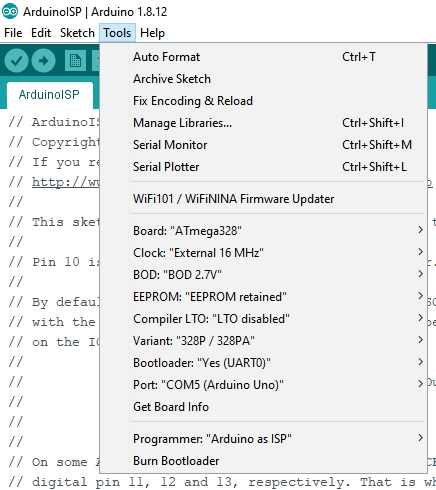
These settings should remain same
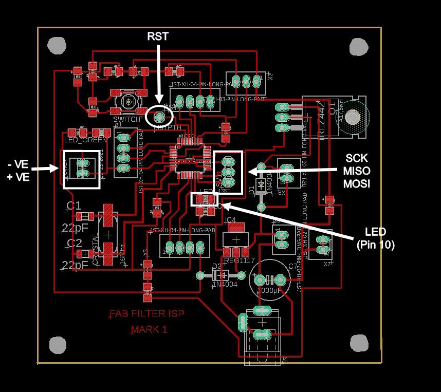
Like the last pcb i have also keep in mind the pins for programming
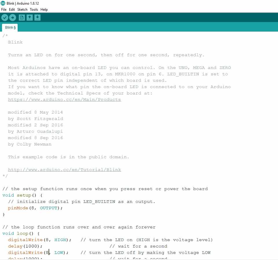
Again Blink code worked perfectly following the above steps
/*
Blink

Turns an LED on for one second, then off for one second, repeatedly.

Most Arduinos have an on-board LED you can control. On the UNO, MEGA and ZERO
it is attached to digital pin 13, on MKR1000 on pin 6. LED_BUILTIN is set to
the correct LED pin independent of which board is used.
If you want to know what pin the on-board LED is connected to on your Arduino
model, check the Technical Specs of your board at:
https://www.arduino.cc/en/Main/Products


This example code is in the public domain.

http://www.arduino.cc/en/Tutorial/Blink
*/

// the setup function runs once when you press reset or power the board
void setup() {
   // initialize digital pin LED_BUILTIN as an output.
      pinMode(8, OUTPUT);
          }

  // the loop function runs over and over again forever
 void loop() {
 digitalWrite(8, HIGH);   // turn the LED on (HIGH is the voltage level)
delay(1000);                       // wait for a second
digitalWrite(8, LOW);    // turn the LED off by making the voltage LOW
 delay(1000);                       // wait for a second
 }
 }
 }
I am listing the blink code her in case you require to use the same code
Code explanation
Well this is the most basic code you can find in the examples , its basic purpose is to command the controller to increase and decrease the amount of voltage on the one specific pin that we defined
            {
             digitalWrite(led, HIGH);   // turn the LED on (HIGH is the voltage level)
             delay(1000);               // wait for a second
             digitalWrite(led, LOW);    // turn the LED off by making the voltage LOW
            delay(1000);               // wait for a second
             }
Inside the loop function, the commands first of all turn the LED pin on (HIGH), then 'delay' for 1000 milliseconds (1 second), then turn the LED pin off and pause for another second.
This code has delay of 1000 micro-second or you can say 1 sec
Please see what happens , when i reduced the delay to 100 micoro-second , the rate of blinking increases as the time interaval btw voltage drop and voltage up decreases
            {
            digitalWrite(led, HIGH);   // turn the LED on (HIGH is the voltage level)
            delay(100);               // wait for a micro - second
            digitalWrite(led, LOW);    // turn the LED off by making the voltage LOW
            delay(100);               // wait for a micro - second
            }
Programming Neo-echo board using the FAB tiny isp
As my insructor commented that i haven't used Fabtiny isp which i made in week to program anything so , i thought i should use fabtiny isp as a programmer and program this board
The steps are almost identical to how you program to program attiny 44 based pcb
Open an blink code by clickin on FILE >> EXAMPLES >> BLINK , and change its led pin to pin 8 , thats what i have given on my board
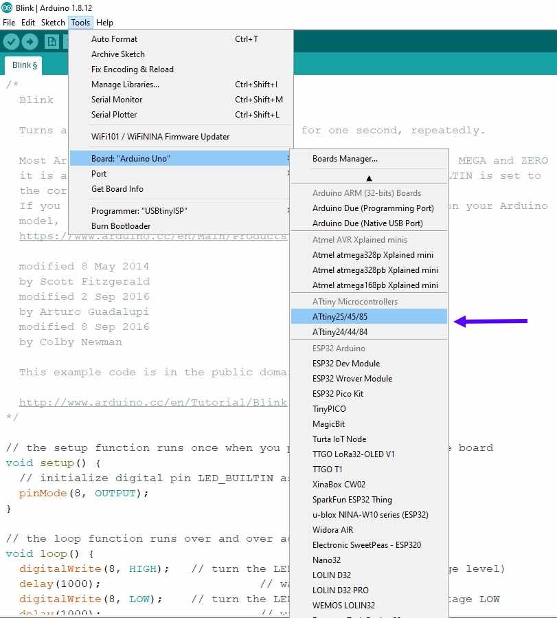
Select board to attiny 45 , as i have mention in my documentation
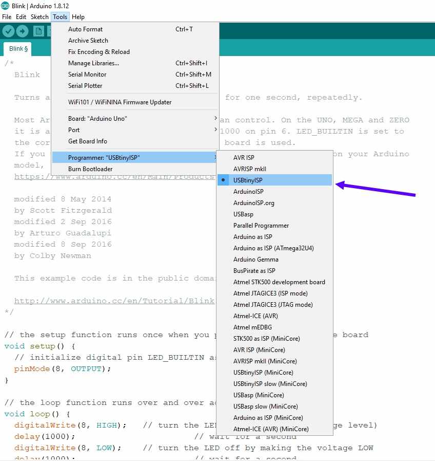
Then change the programmer to USBtinyisp
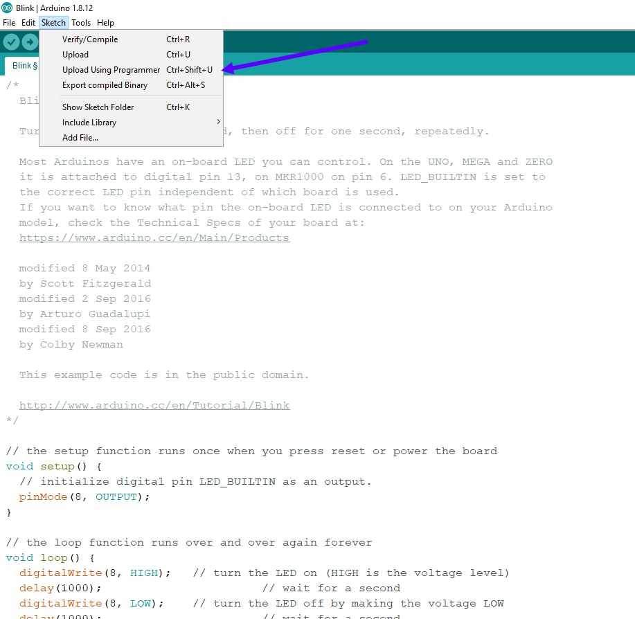
Then upload the code using UPLOADING USING PROGRAMMER command
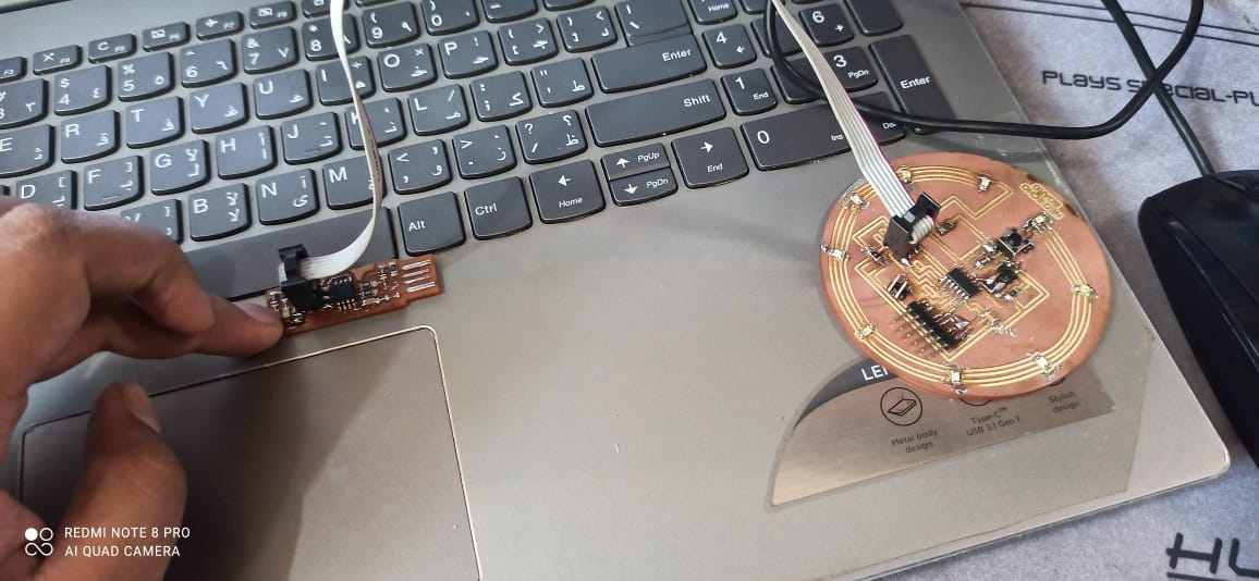
For connections you required a 2 X 3 female ribbon cable or you can wire it using Female to Female jumpers
And connect the FABtinyisp to your system and upload the programme
As you can see through the video
Group Assignment:
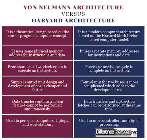
Our assignment was to compare the performance and development workflows for other architectures
Architecture of a micro computer or a micro controller refers to the a>rrangement of the CPU with respect of the
RAM and ROM. Hence, the Von-Neuman and Harvard architecture are the two ways through which the micro controller can have its arrangement of the CPU with RAM and ROM.
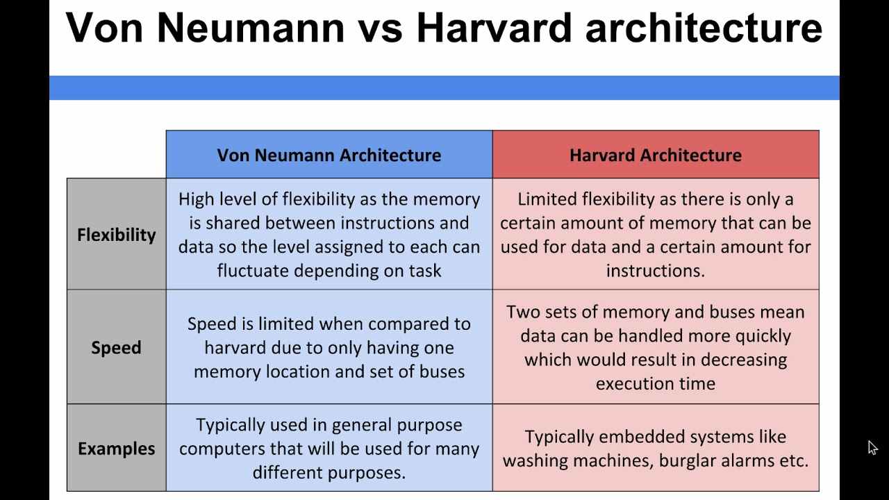
Harvard architecture
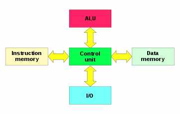
The Harvard architecture is a computer architecture with physically separate storage and signal pathways for instructions and data. The term originated from the Harvard Mark I relay-based computer, which stored instructions on punched tape (24 bits wide) and data in electro-mechanical counters. These early machines had data storage entirely contained within the central processing unit, and provided no access to the instruction storage as data. Programs needed to be loaded by an operator; the processor could not initialize itself.
Today, most processors implement such separate signal pathways for performance reasons, but actually implement a modified Harvard architecture, so they can support tasks like loading a program from disk storage as data and then executing it.
Applications and features of Harvard Architectures
The principal advantage of the pure Harvard architecture—simultaneous access to more than one memory system—has been reduced by modified Harvard processors using modern CPU cache systems. Relatively pure Harvard architecture machines are used mostly in applications where trade-offs, like the cost and power savings from omitting caches, outweigh the programming penalties from featuring distinct code and data address spaces. Digital signal processors (DSPs) generally execute small, highly optimized audio or video processing algorithms. They avoid caches because their behavior must be extremely reproducible. The difficulties of coping with multiple address spaces are of secondary concern to speed of execution. Consequently, some DSPs feature multiple data memories in distinct address spaces to facilitate SIMD and VLIW processing. Texas Instruments TMS320 C55x processors, for one example, feature multiple parallel data buses (two write, three read) and one instruction bus. Microcontrollers are characterized by having small amounts of program (flash memory) and data (SRAM) memory, and take advantage of the Harvard architecture to speed processing by concurrent instruction and data access. The separate storage means the program and data memories may feature different bit widths, for example using 16-bit wide instructions and 8-bit wide data. They also mean that instruction prefetch can be performed in parallel with other activities. Examples include the PIC by Microchip Technology, Inc. and the AVR by Atmel Corp (now part of Microchip Technology).
The speed aspect: A lot has been discussed about the Harvard architecture, but without the speed any architecture can’t be accepted. But in case of the Havard architecture the manufacturers have designed the architecture in such a way that it will be able to process the data with a much higher speed. Yes, all care has been taken so that the architecture can process data with a high speed. By implementing the same formula the modern days CPU are being manufactured so that the new CPU can run with a much faster sped and can also process the data effectively. The concept of the CPU cache is also being implemented while designing the Harvard architecture.
Von Neumann Architecture
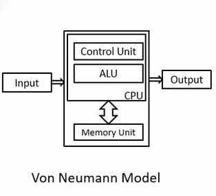
The von Neumann architecture, which is also known as the von Neumann model and Princeton architecture, is a computer architecture based on the 1945 description by the mathematician and physicist John von Neumann and others in the First Draft of a Report on the EDVAC. This describes a design architecture for an electronic digital computer with parts consisting of a processing unit containing an arithmetic logic unit and processor registers; a control unit containing an instruction register and program counter; a memory to store both data and instructions; external mass storage; and input and output mechanisms. The meaning has evolved to be any stored-program computer in which an instruction fetch and a data operation cannot occur at the same time because they share a common bus. This is referred to as the von Neumann bottleneck and often limits the performance of the system. The design of a von Neumann architecture machine is simpler than that of a Harvard architecture machine, which is also a stored-program system but has one dedicated set of address and data buses for reading data from and writing data to memory, and another set of address and data buses for instruction fetching.
Applications and features of Von Neumann Architecture
The Von Neuman architecture has got extensive application in everyday life. Keeping in mind the extensive application the Von Neuman architecture has been introduced as a subject in the engendering degree. From the third semester engineering students will have the subject as their curriculum. The Von Neuman architecture consists of some important features and here we will have a detailed elaboration to the features.
Control Unit: This unit is mainly responsible for the controlling aspect. All the data stored in the memory and during the processing of data the control unit plays the role and it manages the data flow.
In fact, to be more typically it is “One At A Time”. The control unit follows the principle of the One At A Time and accordingly it process all the data.
nput– output: Like all electronics devices the Von Neuman architecture also has an input/output architecture. It is the basic function is same and nothing specially has been designed for the input and
output architecture. With the Input and output device on a person can communicate with the device.
ALU: ALU or the Arithmetic Logic Unit has a great importance in the Von Neuman architecture. Any sort of addition, subtraction, multiplication and division of the data will be carried out by this ALU.
In addition to that any other kind of algorithmic function and activities will be carried out by the ALU. These are the basic aspect of the Von Neuman architecture which you must aware of.
FAB FILTER MARK 1 by
PULKIT TALWAR is licensed under
CC BY-NC-SA 4.0
![]()
![]()
![]()
![]()