Final Project
IMPORTANT NOTE : ALL OF MY IMAGES ARE POP UP IMAGES , IF YOU HAVE ANY PROBLEM READINGS THOSE IMAGES , PLEASE CLICK ON THEM AND THEY WILL ENLARGE AUTOMATICALLY AND YOU CAN READ THEM EASILY
Fab Filter
I intended to build a smart moduler air filter which can be easily kept at small places or hang on the walls and easily move from one place to another plus it will be smart as it will increase or decrease the speed of fan on the different ppm lvl , whihc will be calculated using an ppm sensor
Motive :The basic motive behind designing something like this was , as you all knows that the lvl of air pollution is much higher then every other countries , and the clg i study in is situated inside one of the biggest industrial area , in my region which also contribute to high pollution lvl and for last 4 years , we have experiece this adverse enviroment , so i decided totackle this problem by adding these small moduler air filter to my class room , so it can make some difference in the pollution lvl.

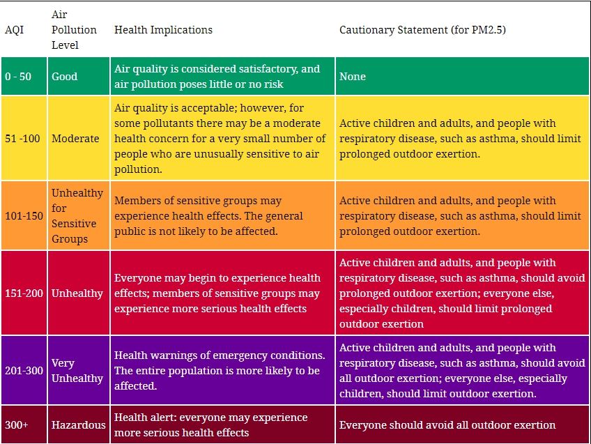
As you can see from the list , india has one of the most polluted cities in the world
Components which i planned to add
* D.c Brushless fan
* 4 different air filter
* PCB circuit
* PPM meter
* DHT 11 sensor
* LCD screen
I have documented things like BOM , who has done what , and what material i am going to , all of it is on
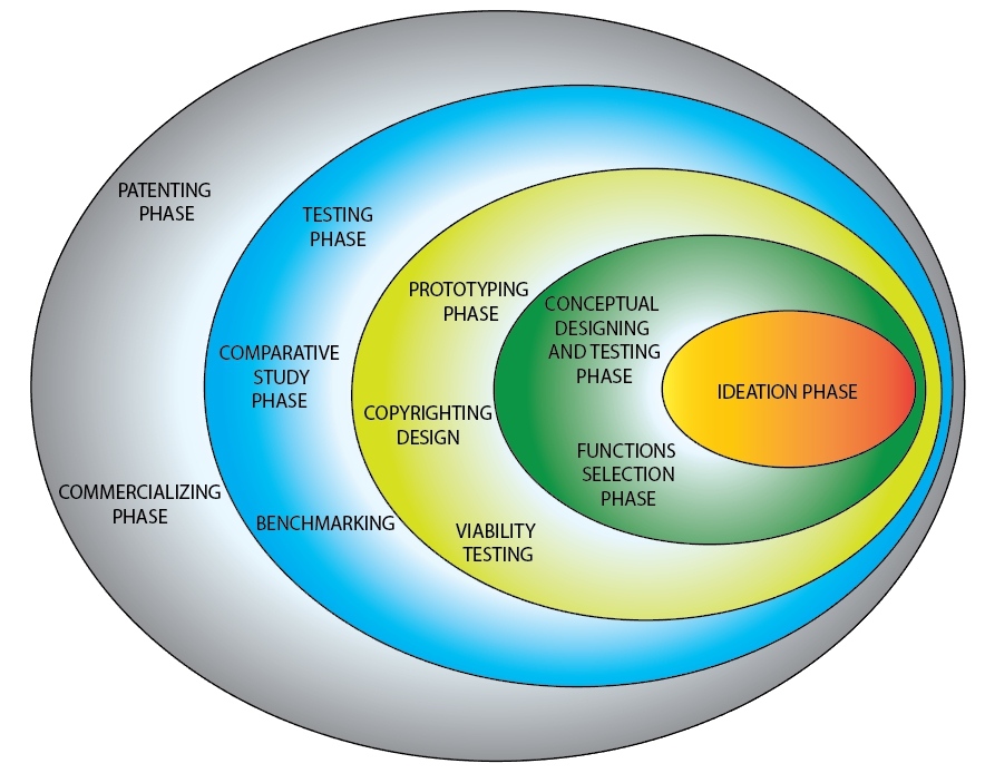
This is the work plan which i made , for future workflow
Designing
Conceptual Design
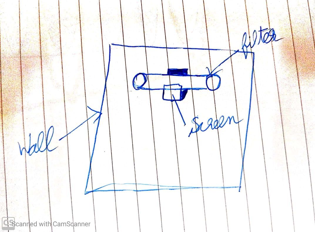
This is something which i have designed on paper , the purpose of this design was to bring the idea from mind to paper s , i can start working further
As from design you can see that i have made a wall and placed my filter on the wall ,as initially i though to make it wall mount
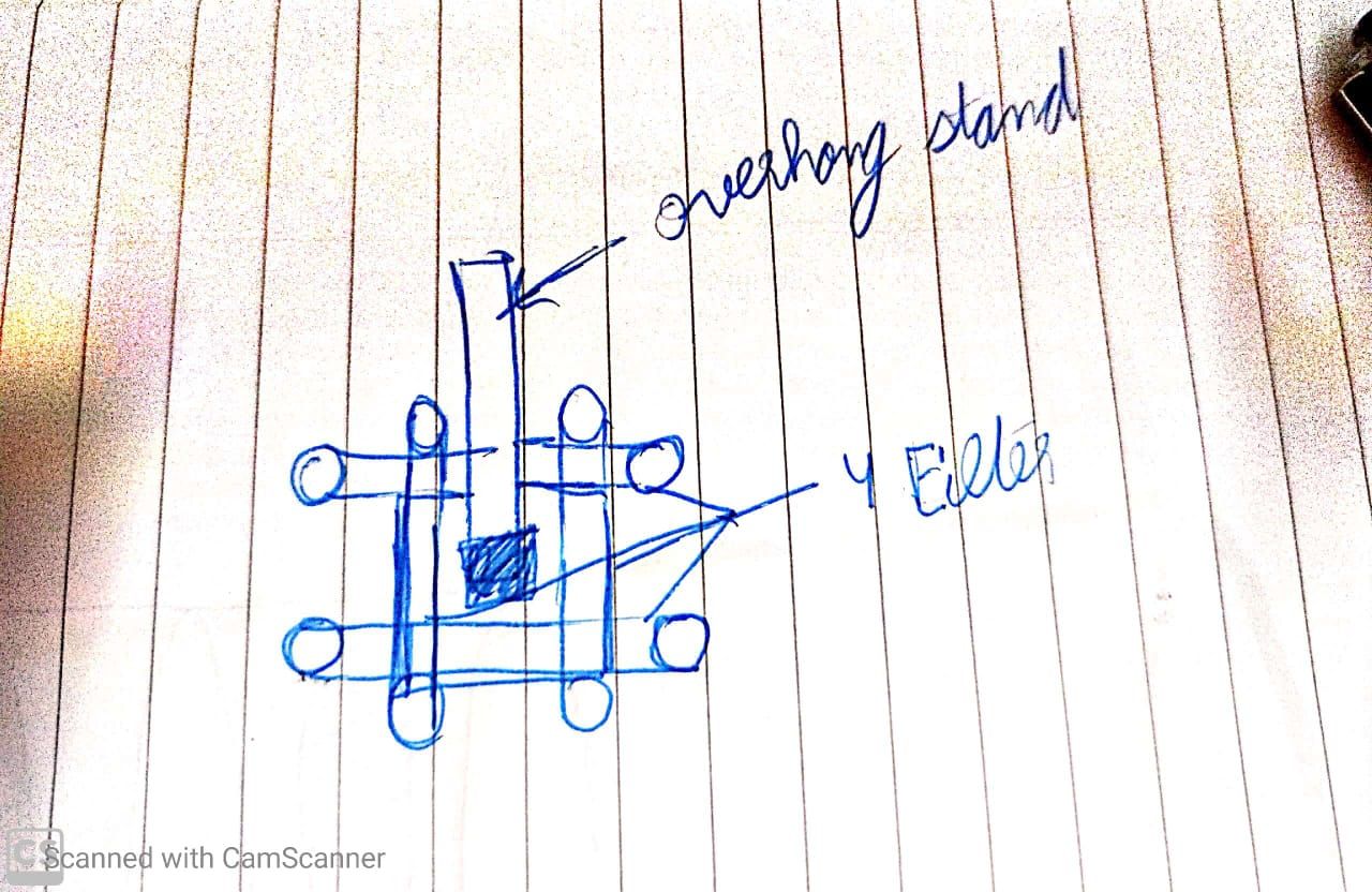
I also draw this other configuration in which i have placed 4 filters on an overhang rod
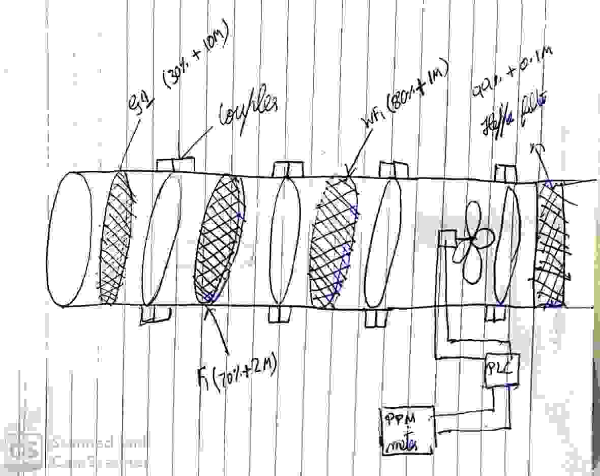
And this image shows the inner component of my filter , for this purpose i required to consult a lot of things with my professer D.r Krishnendu Roy sir , as he has a very vast experience in this field
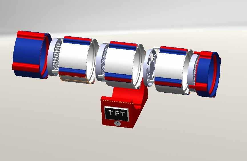
As you can see this is an pre-mature design of my project. basically my plan is to make an affordable air purifier which incorpaorate an ppm meter which is designed to display the ppm level and the fan will be controlled by that ppm level and the ppm level increasethen the speed of fan also increases
Initial Designing
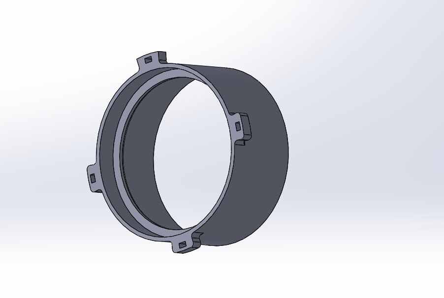
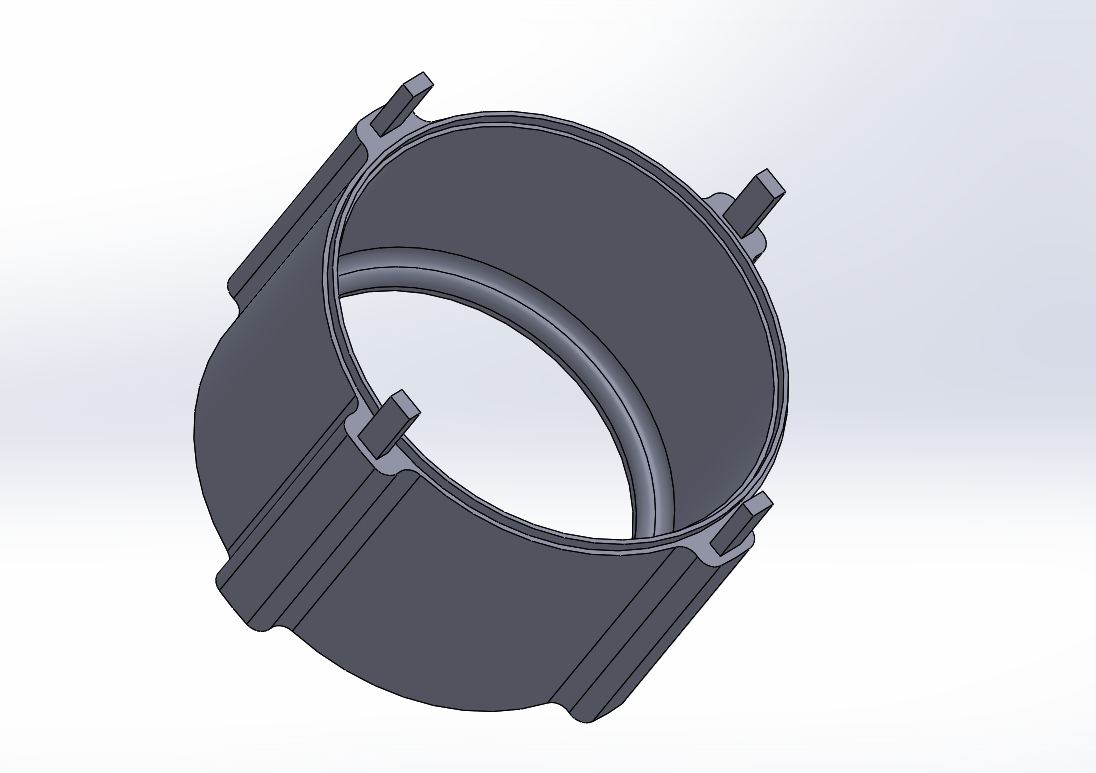
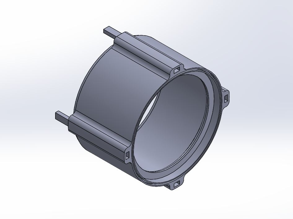
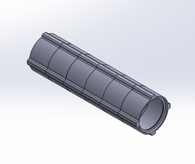
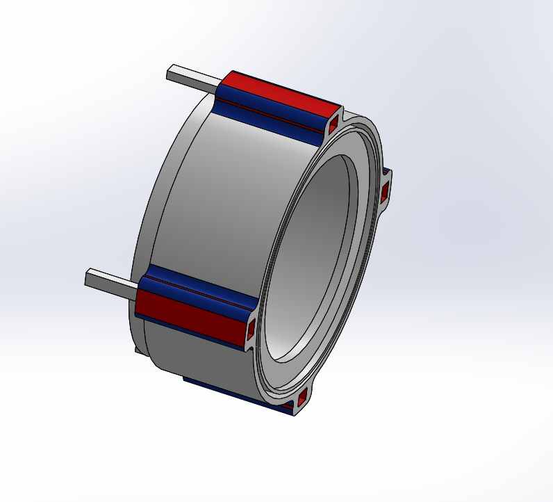
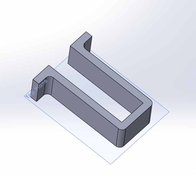
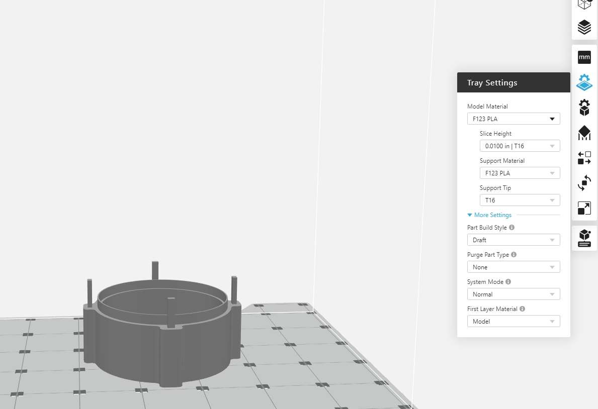
* This is the first part of the prototype part and it will act as head or top piece , it has 100 mm diameter and 70 mm length
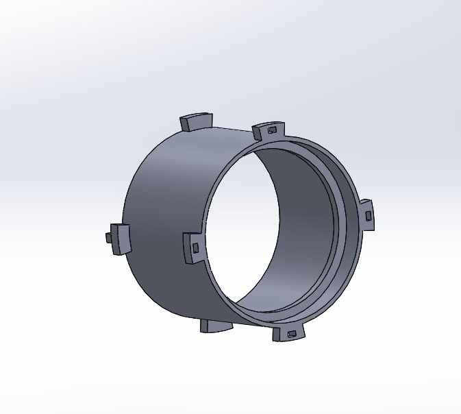
* All other modules ranging from C2-C6 are made copy of this part here you can see that it has both male and female part
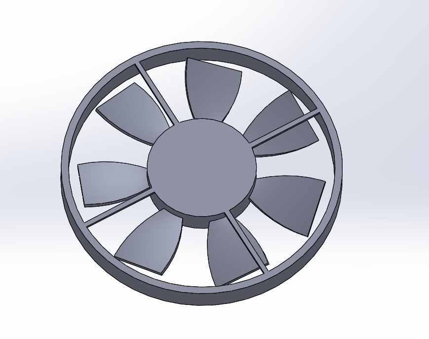
* It is an 12v DC fan which will be used to create suction and able to suck the impure air
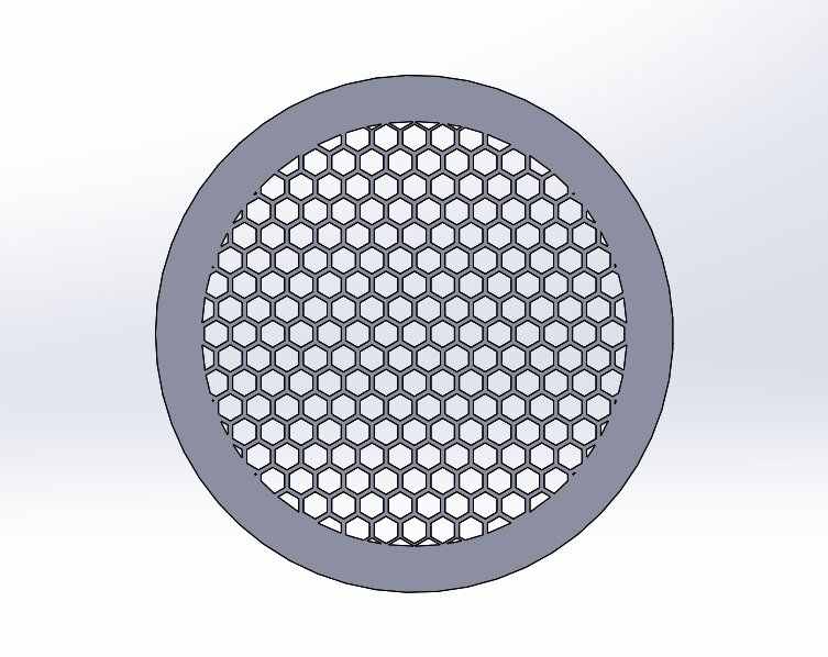
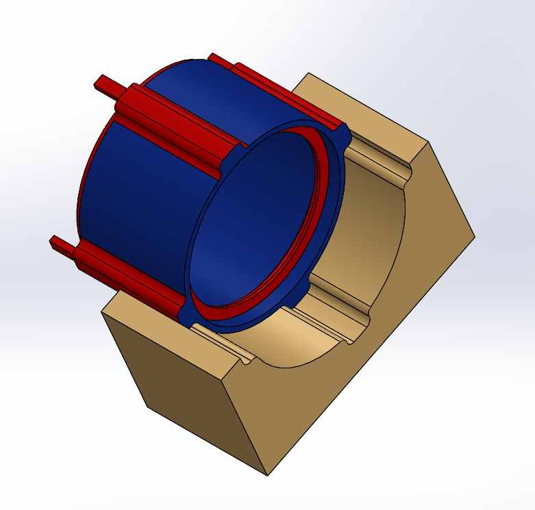
This image represents Filter housing ,its just only for show
Initially it was planned that it will incorporate 4 filters and they are as follow
G1 Filter: this will be the first filter and it will be able to to clean air upto 30% and will deal upto air particle of 10 micron size
F1 Filter: this will be the 2 filter in the path of air and it will be able to clean air upto 70% and can deal with particle upto 2 micron
WF1 Filter: this will be the 3rd filter in the series and will purify air upto 80% and will be used to deal with the air pollutent of 1 micron
High efficiency particulate air (HEPA), originally called high-efficiency particulate absorber but also sometimes called high-efficiency particulate arresting or high-efficiency particulate arrestance, is
a type of air filter. Filters meeting the HEPA standard have many applications, including use in clean rooms for IC fabrication, medical facilities, automobiles, aircraft and homes. The filter must satisfy certain
standards of efficiency such as those set by the United States Department of Energy (DOE).
Varying standards define what qualifies as a HEPA filter. The two most common standards require that an air filter must remove (from the air that passes through) 99.95% (European Standard) or 99.97% (ASME
standard) of particles that have a size greater than or equal to 0.3 μm
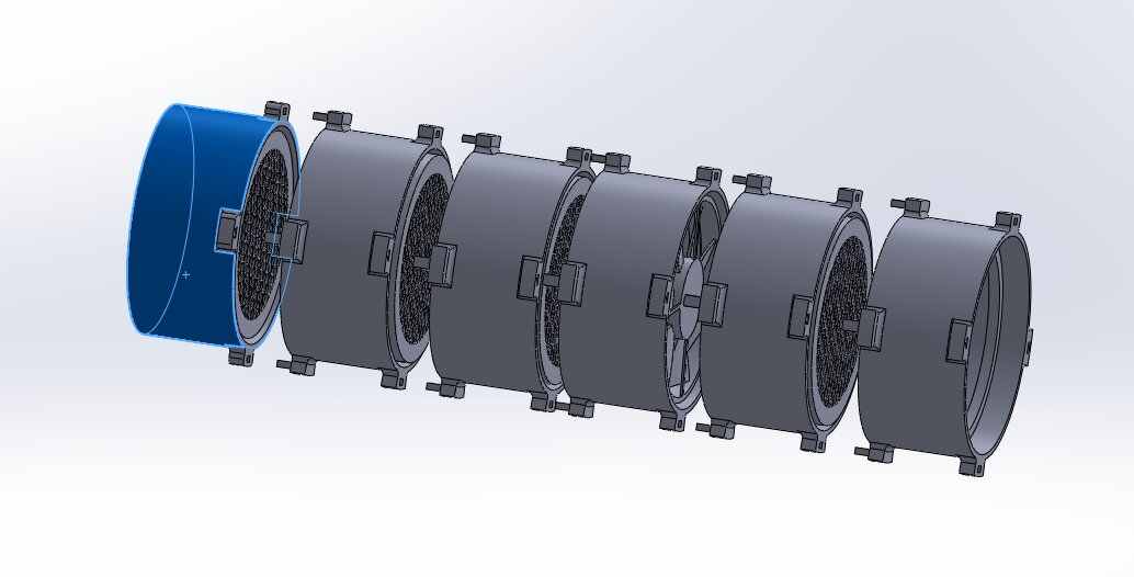
Through this image you can see that how they will be interlinked to each other
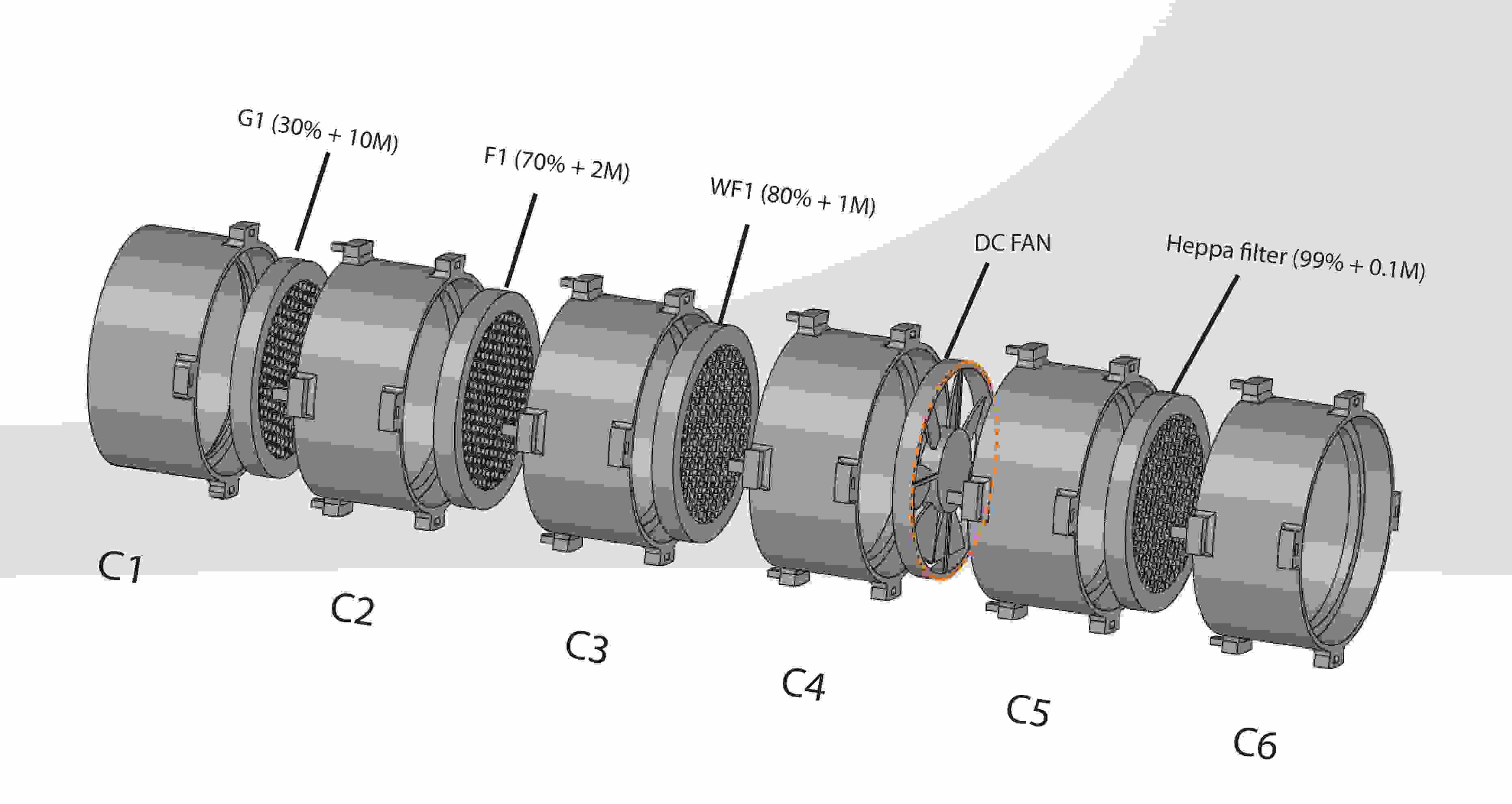
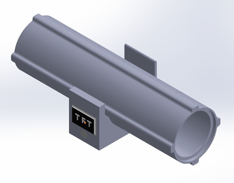
* This is an full detailed image of all the parts associated with the air purifier
Intermediate Design
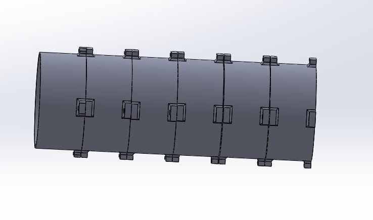
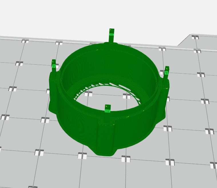
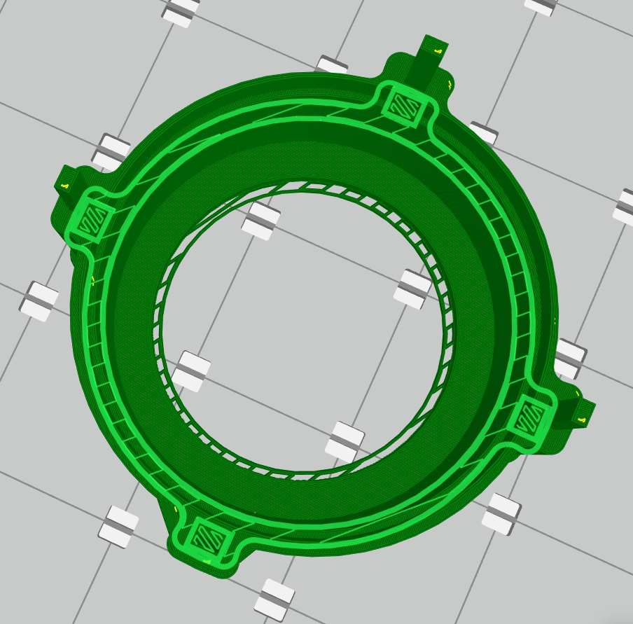
Through this image you can see that i have made some mpdification in the design by making it more asthetic as well as i added little slots in geometry so i can connect them easily
Same goes for this interconnection module as well
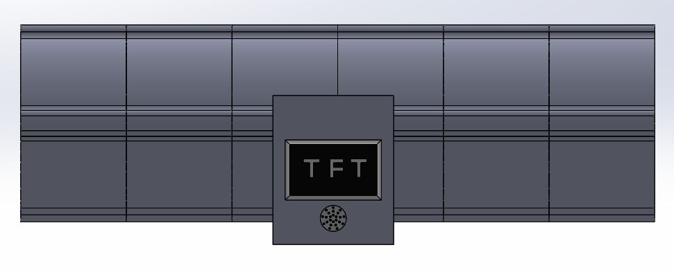
I also made the electronics box and screen mounting
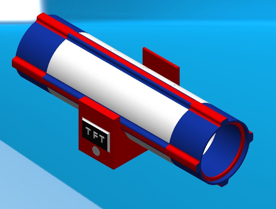
How its look i added some colour to it so it can look more presentable as a CAD design
Final Designing
After I printed the parts i saw this that the size and printing time for 1 piece was too much and i require 4-5 pieces so , i reduces the length of the module
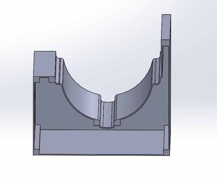
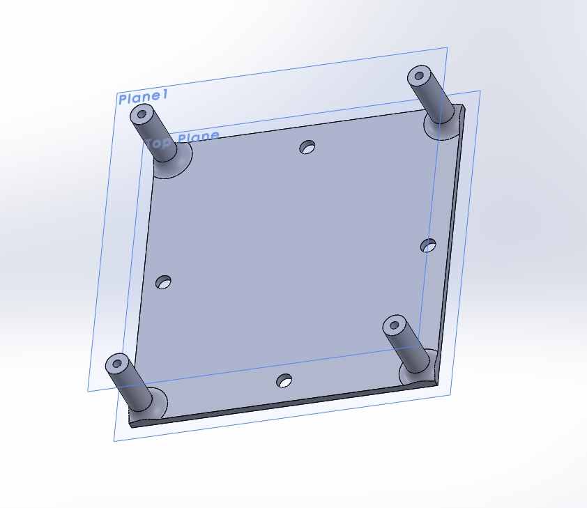
The filter module anelectronic box is required to fit on each other so they have this kind of geometry
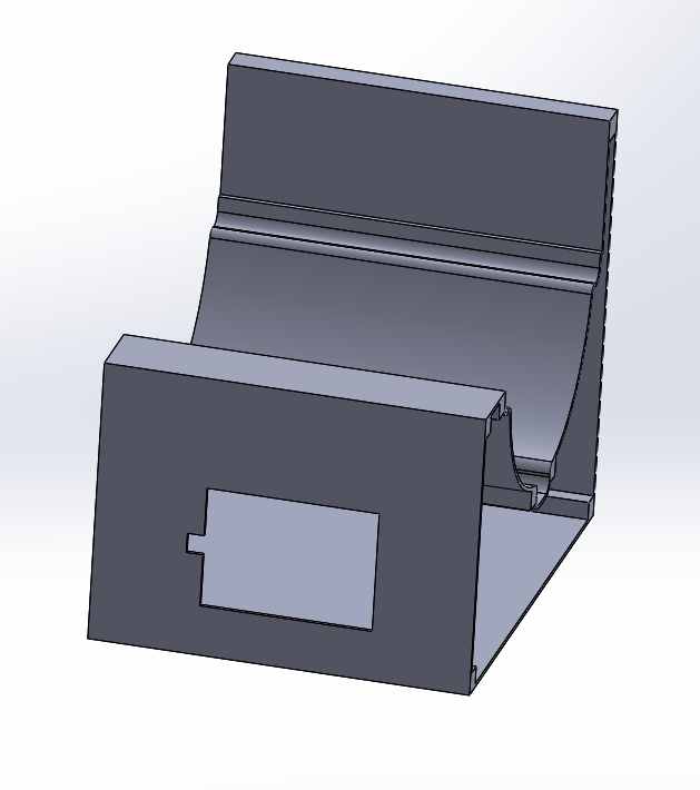
This will be my electronix box it has a rough size of 100mm length and 140 mm of breadth and it should house my pcb , my ppm sensor , my dht sensor and my tft screen
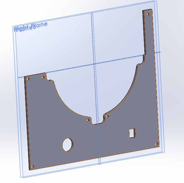
This will be its opening cover which will be attached to the place using screw's as if something goes wrong i can
This was a sort of clamp which i made to clamp my ppm sensor to the place so when integerate all the systems it wont move
This was the mount which i made to mount the pcb and place it int he electronics box
I am attaching all the CAD Files here if you want you can download these files
Fab filter cad3D printing
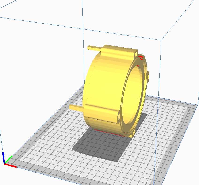
As the designing is completed , now time comes for 3d printing so i can validate interconnectivity btw my design
For this i went through 3 different type of printer
1. Anet A2 plugins
2. Makerbot z18
3. F370
Starting with anet a2 plus , as this is is my personal printer so i thought that i can easily work with my prints from my home
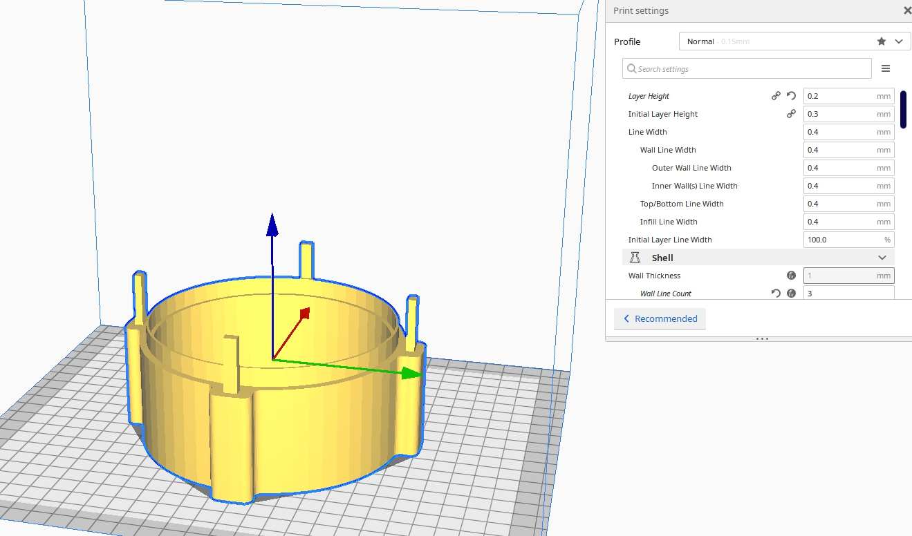
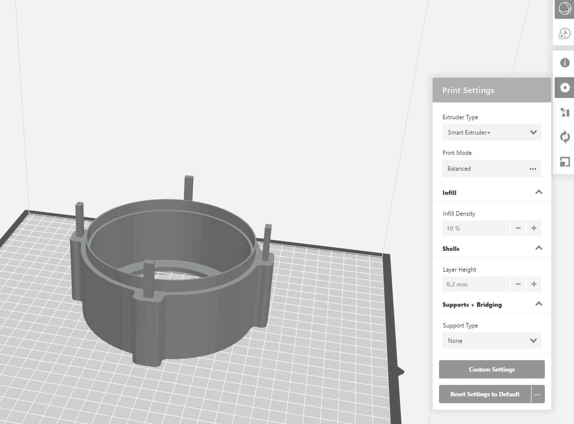
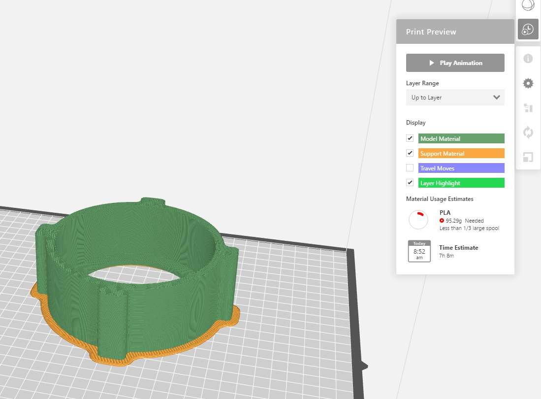
I added stl file for the print in cura software for slicing And kept the layer height to 0.2mm and 15% infill initially
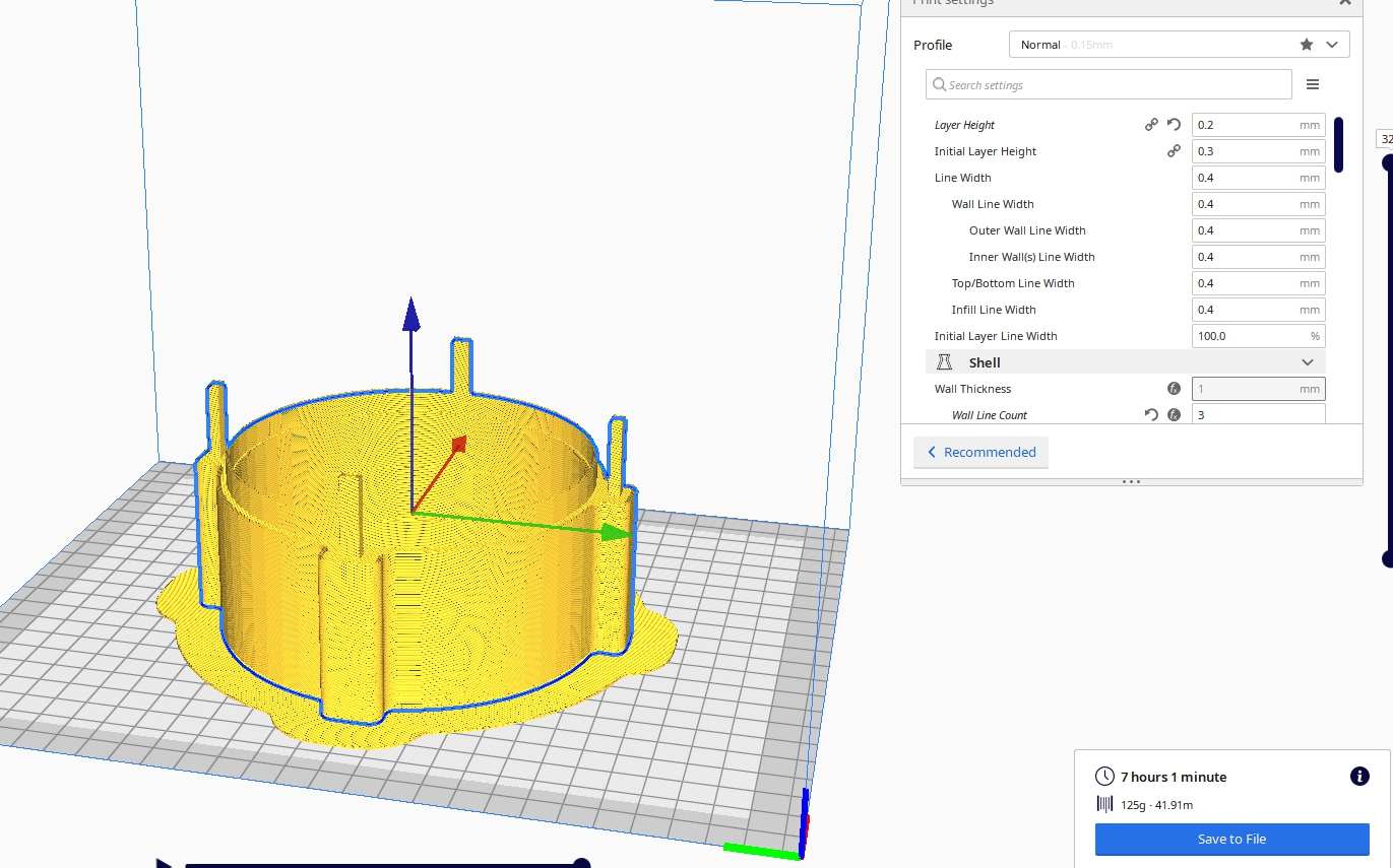
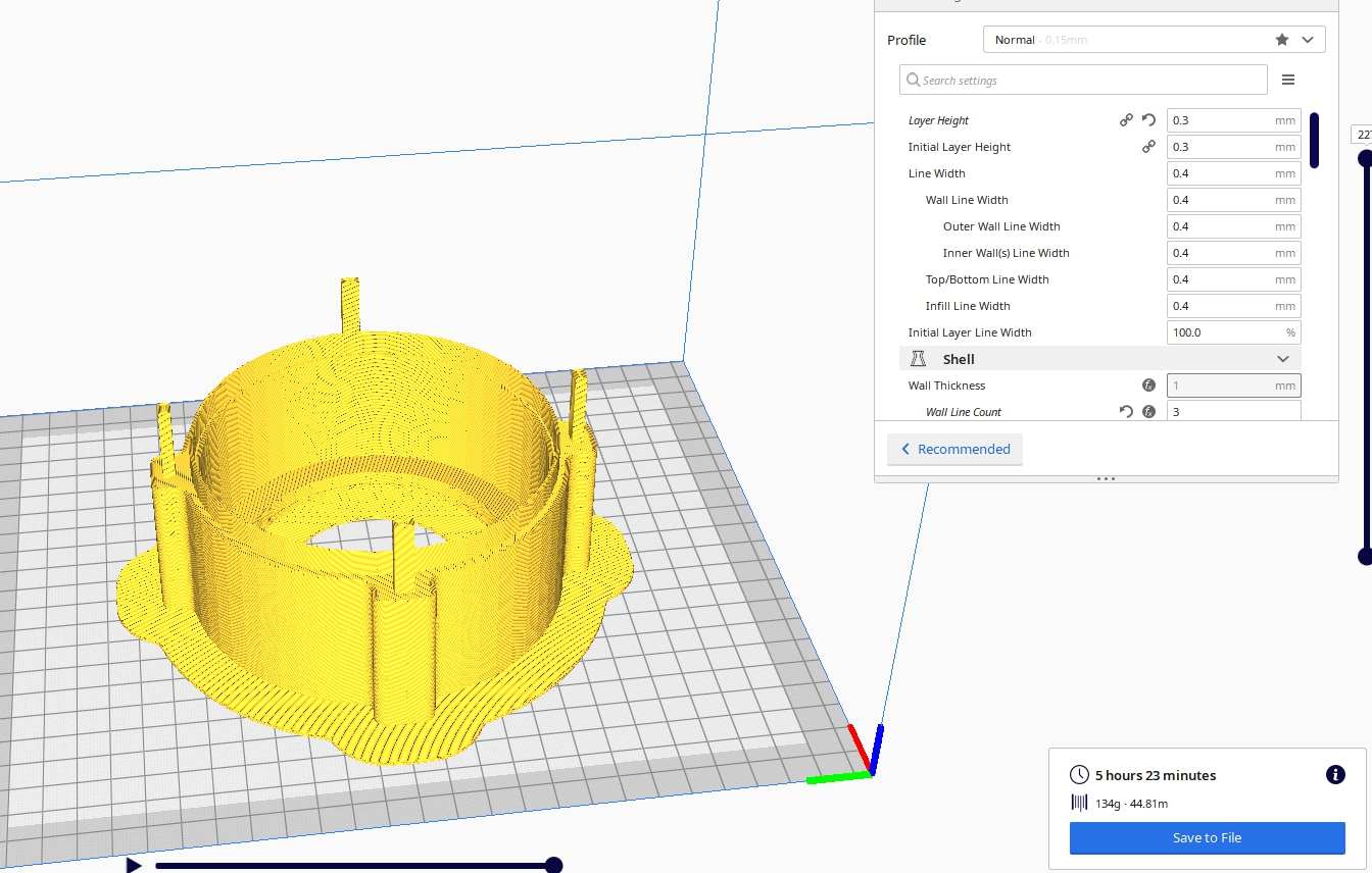
Then i saw that it was taking 7 hours and i thought it is too much for only a test print si i increased the layer height to 0.3 mm and reduce infill to 10% nd got a print around 5hr 30min , si i printed it
I was not happy with the quality as my anet a2 is a DIY printer and i say tha there is merging of 2 layers at some point du to lack f bed levling on my side so i decided not to work on my printer for my particles
Plus i saw that it is very difficult to let the printer work for 5 hrs , during electricity cut
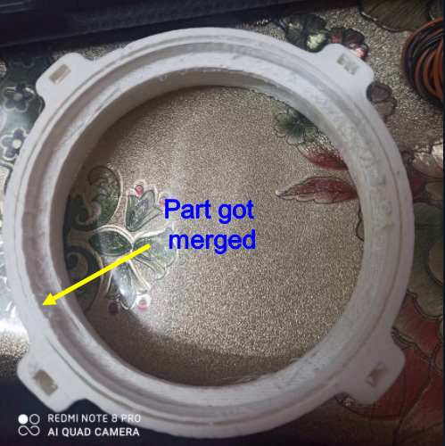
You can see the point on the bottm layer where it merged
Then i switched ti makerbot Z18 , it is a very good printer at our lab so i though it should be better to print from a good calibrated printer
I saw the same result as for 0.2mm layer height and 15% infill , it shows the same time so i thought i should try
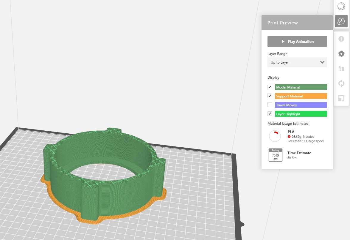
Like last time i again increased the layer height to 0.3mm and the build time reduces
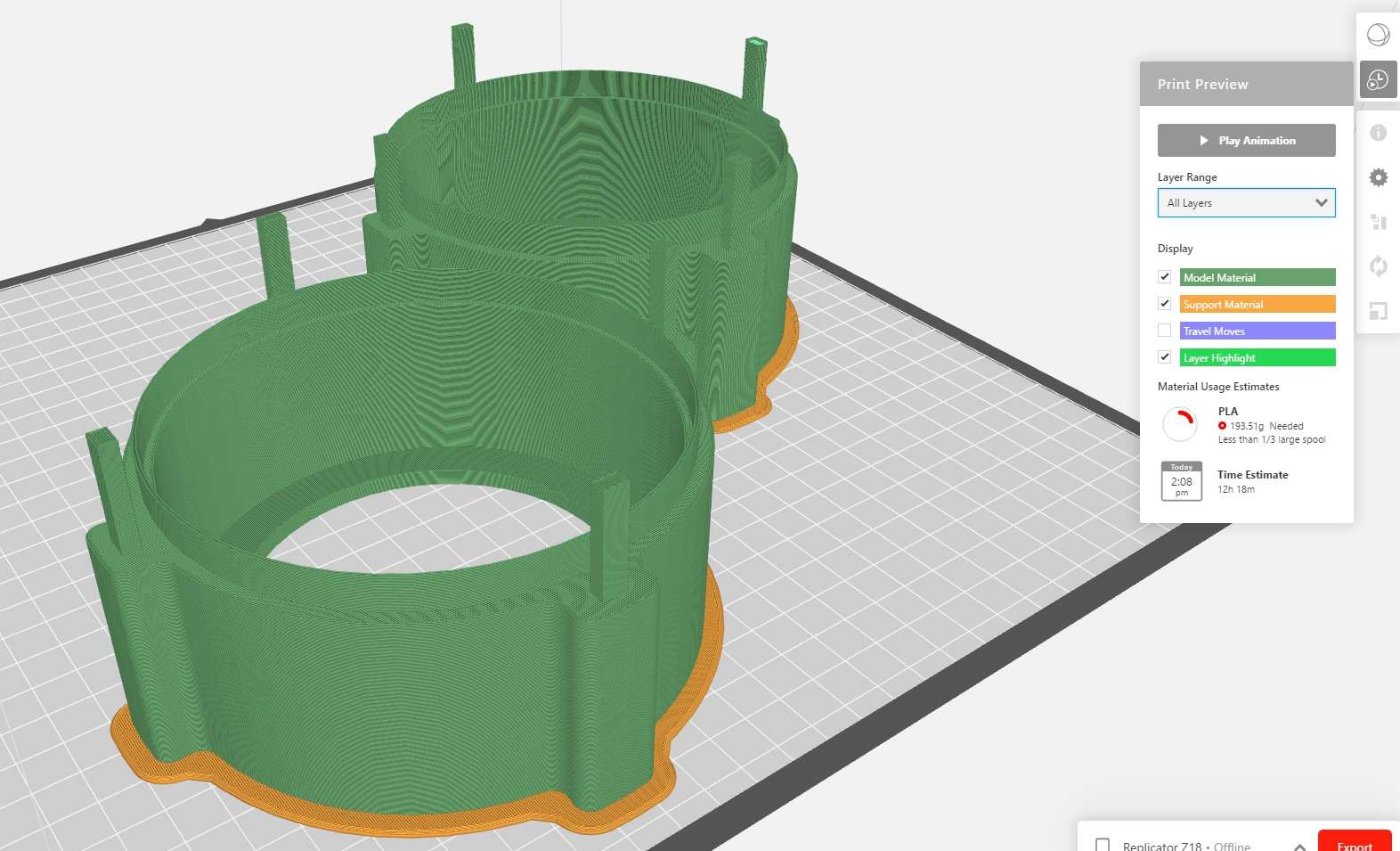
So i added the 2 pieces a tones to print
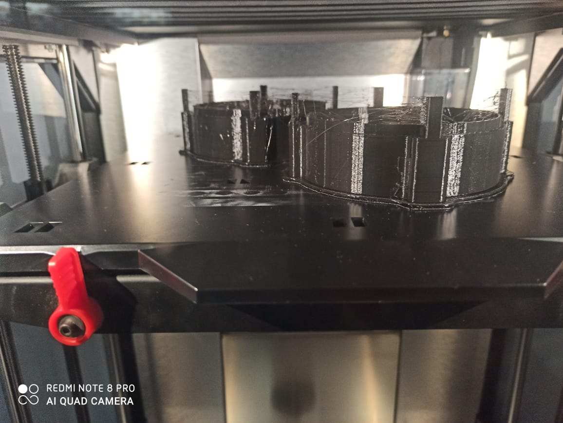
You can see the print after 12hrs
I was not happy with qaulity as n it has lots of strings and there was no smoothness here , my instructor told me that this happened because of the old hot end and there is someamount of material stuck in nozzle
So i needed to switch to 3 printer i.e stratasys f370 , it is a very good printer and can give highest finish possible ,
but like always there was again a problem , that our machine lack of soluble support material , so iwas required to work with only pla
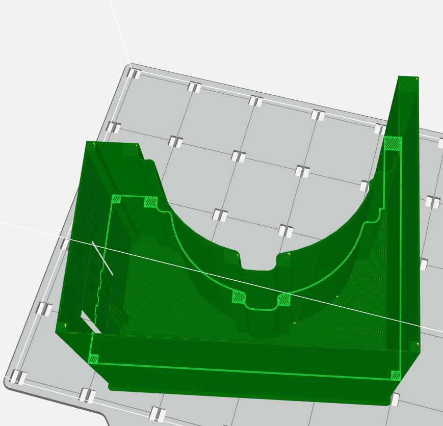
This is the sliced image of the part
When i looked closely i spotted that the slicer software grabcad in the case of pla material doesnt ask about the how much support we want to give , which posses a huge problem
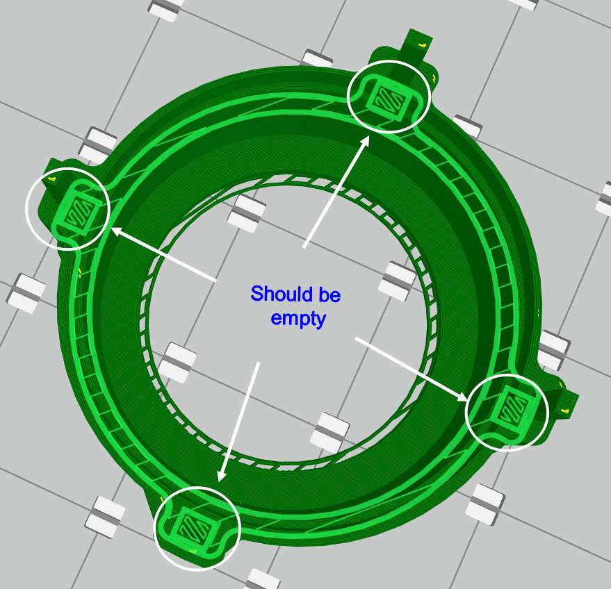
If you closely look on these parts , these were meant to be hollow but they have support building in them which was not shown in any other software slicer
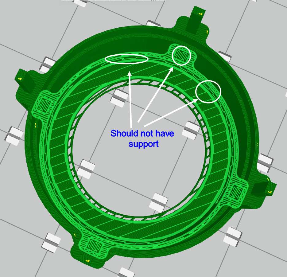
This effects the interlocking capability of my modules so i was only print 1 piece from stratsys which unconviniently i have to place at the bottom
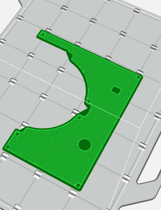
Time to print the electronic boxe , this was a long print due to its big geometry , it took 9hrs 30min to print this , but the mateial consumption was realy nominal
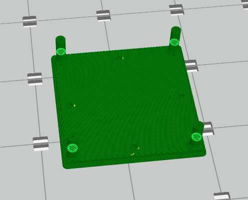
Then i printed its cap
This is a pcb mount which i printed so i can elevate the pcb
PCB making
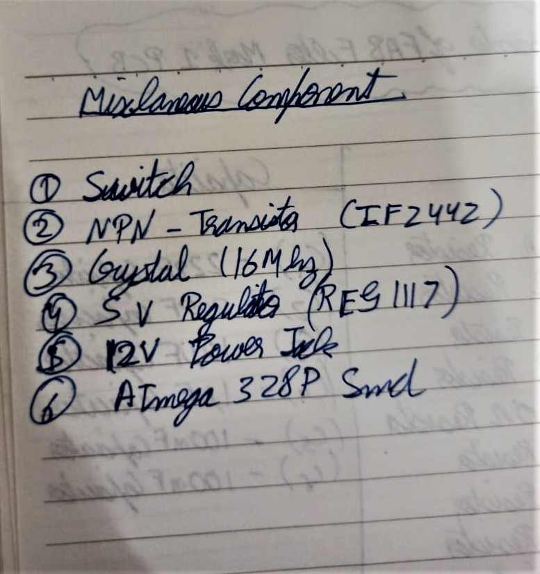
To be graduated i was required to make a custom PCB for my electronics ,which can be used to take input , can provide output , and also can do networking with other systems also
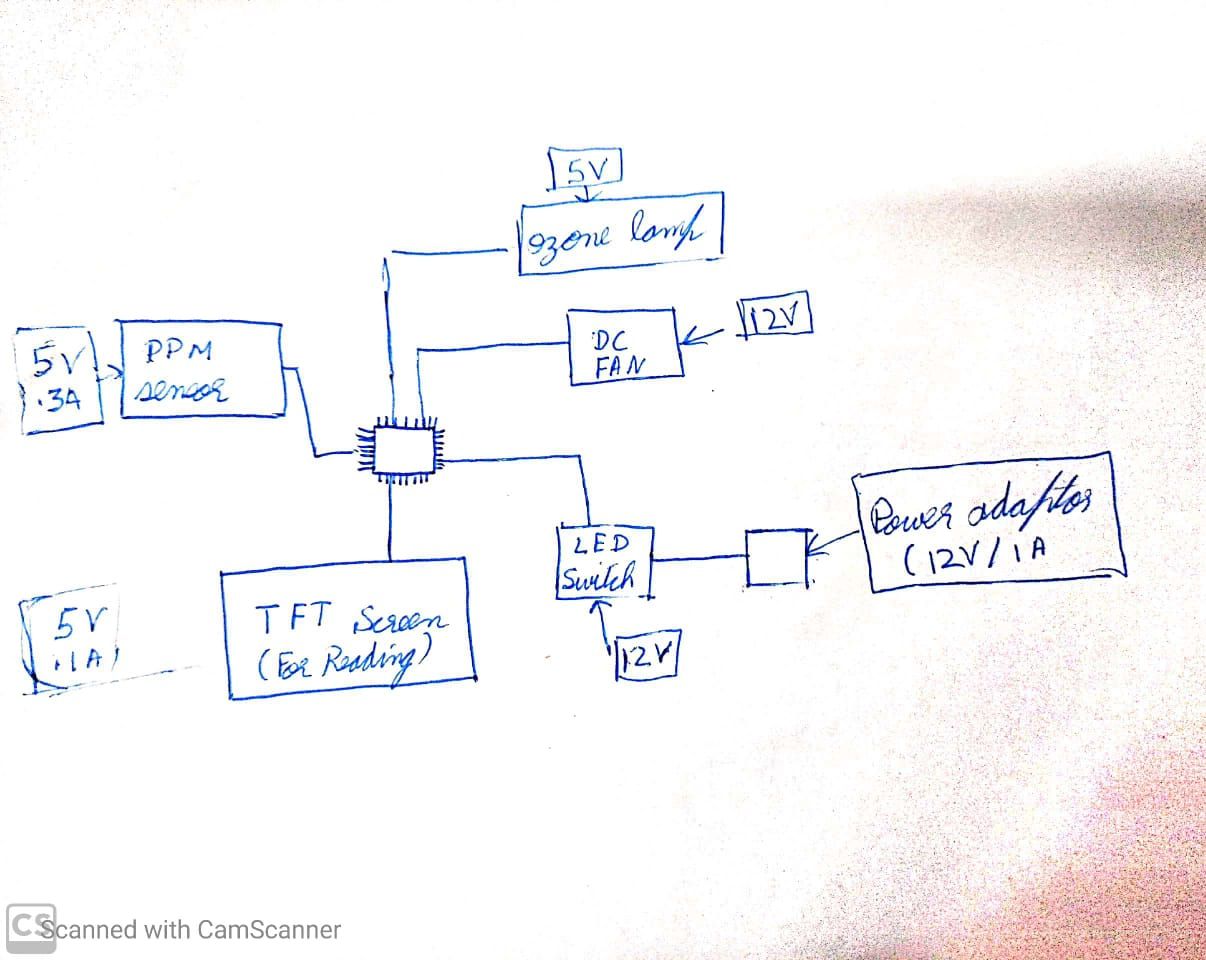
First before going to design something i was required to make a rough schematic like , what will be connected to what , and what are there current requirement as well as on what voltage they work
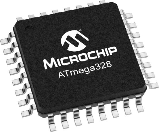
I used Atmega 328p as my main Ic
I have explained about this I.c in detail on this page , if you ike you can go and
see how it works and what are its pinout
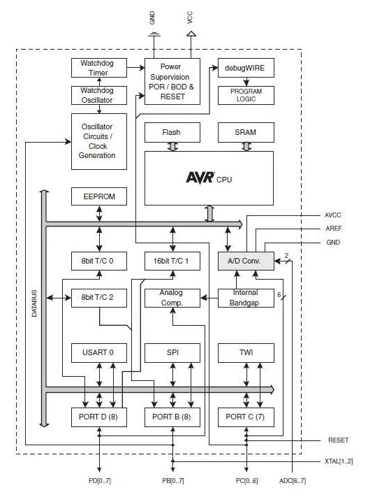
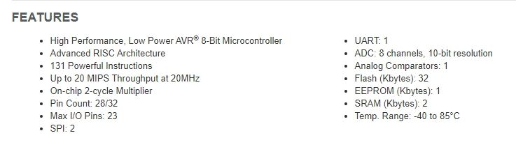
Basic feature of ATMEGA 328P , well the main decision of my choosing this pcb was that , it was easily available in ur lab as well as it the same chipset use in Arduino UNO.
Satshakit
well before i never desined PCB and to start i look to this satshakit , it is a atmega 328p based pcb which was ddesigned by previous year students , with a detailed documention if you like you can go on the original page by clicking on this link
This is the standard schematic of satshakit
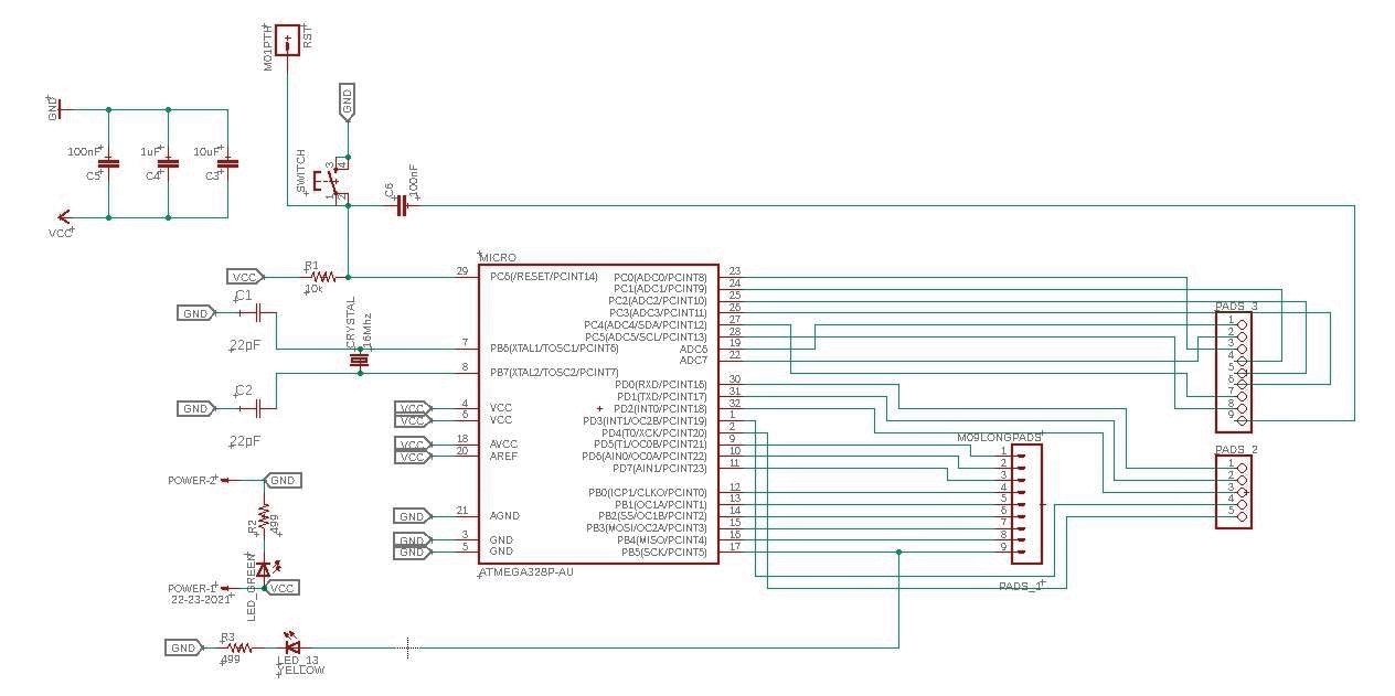
This is the schematic for my PCB
this is my board which i cutted initialy , but i accidently forget to add avrisp pins and without those pins i won't able to program the board , so ineed to add those pins
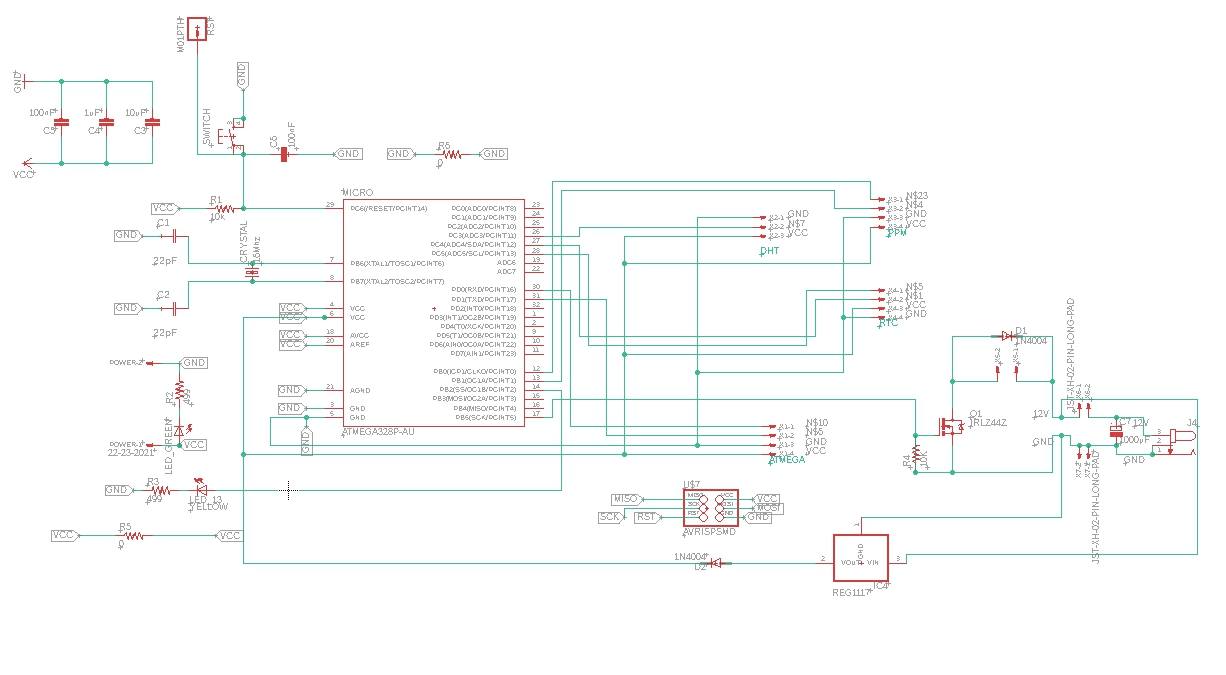
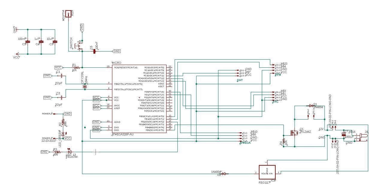
This is my modified schematic which has Avrisp pins which i want
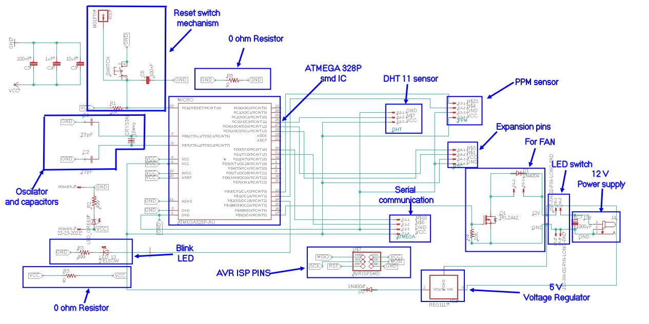
I have in detail explained my schematic
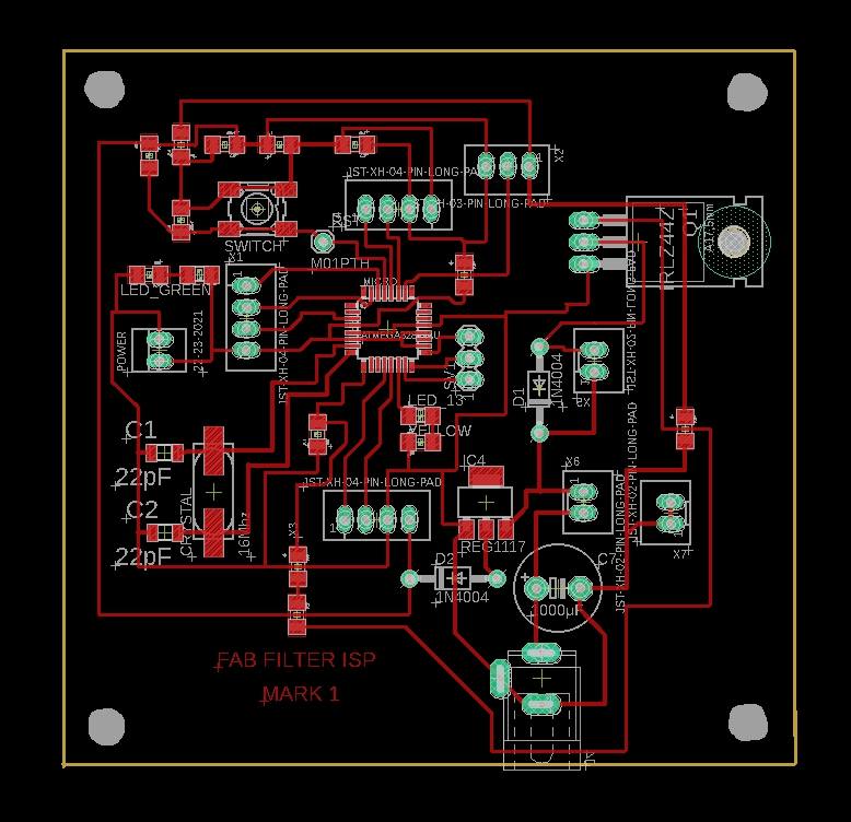
So i modified my board to incorporate those pins as well
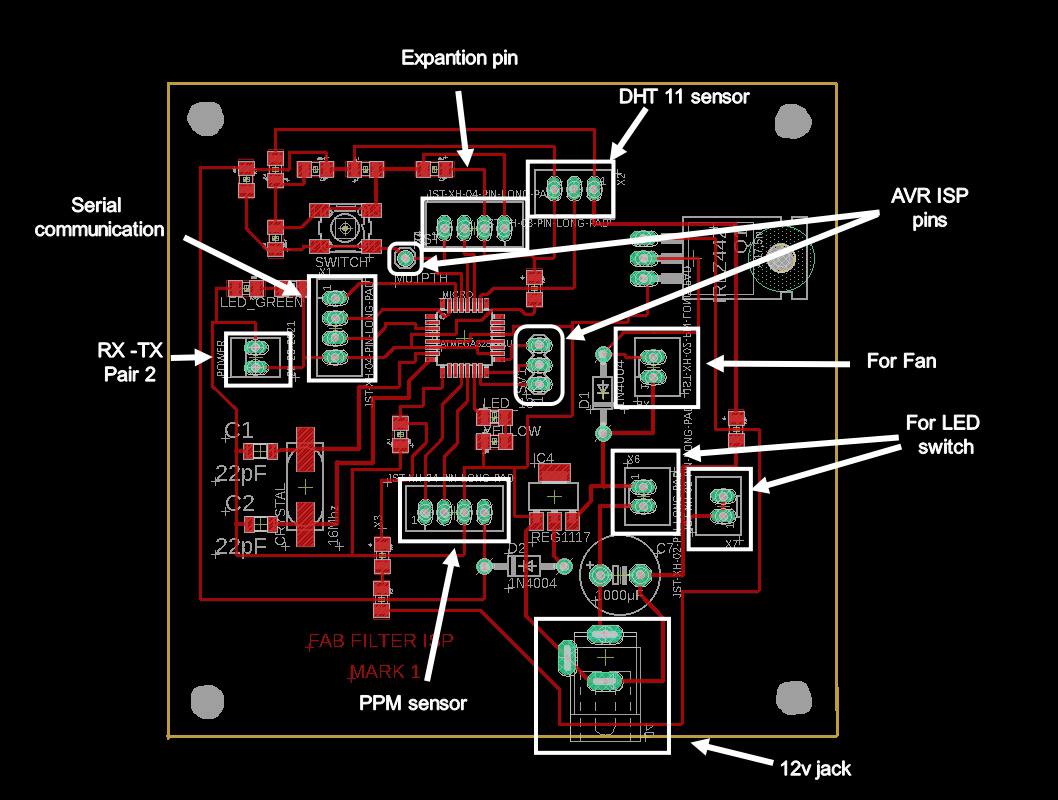
Throught this image all the components of my board
I am attaching all the CAD Files here if you want you can download these files
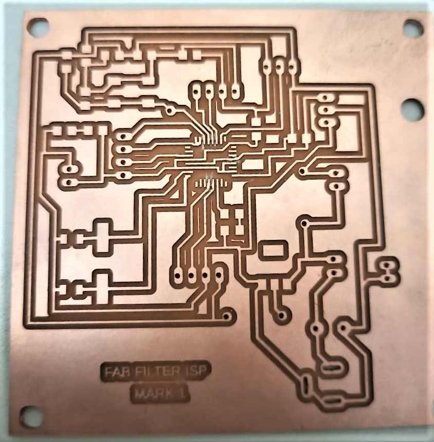
FAB Filter Mark 1 isp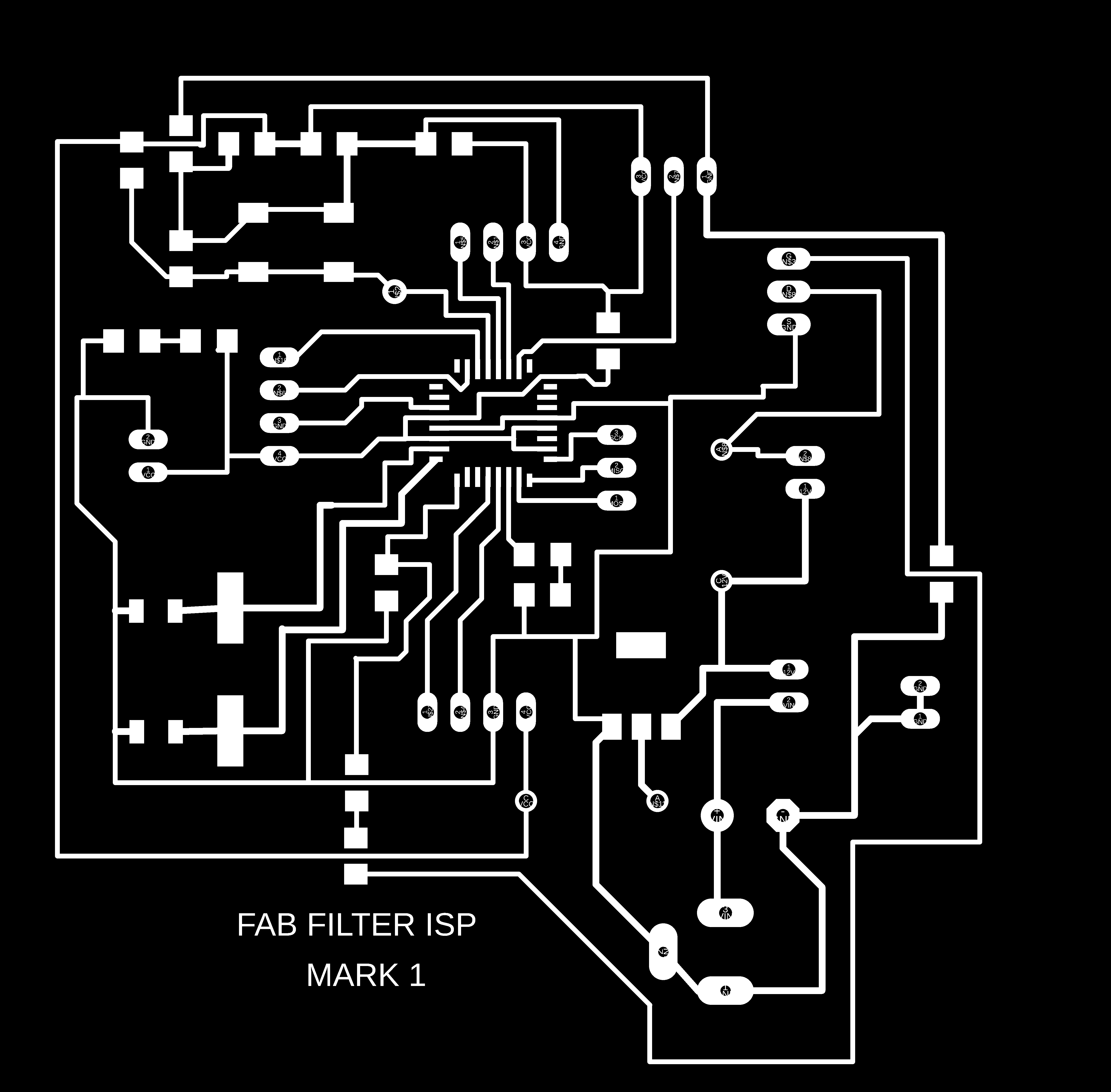
This will be png image for my pcb track which will be milled in srm 20
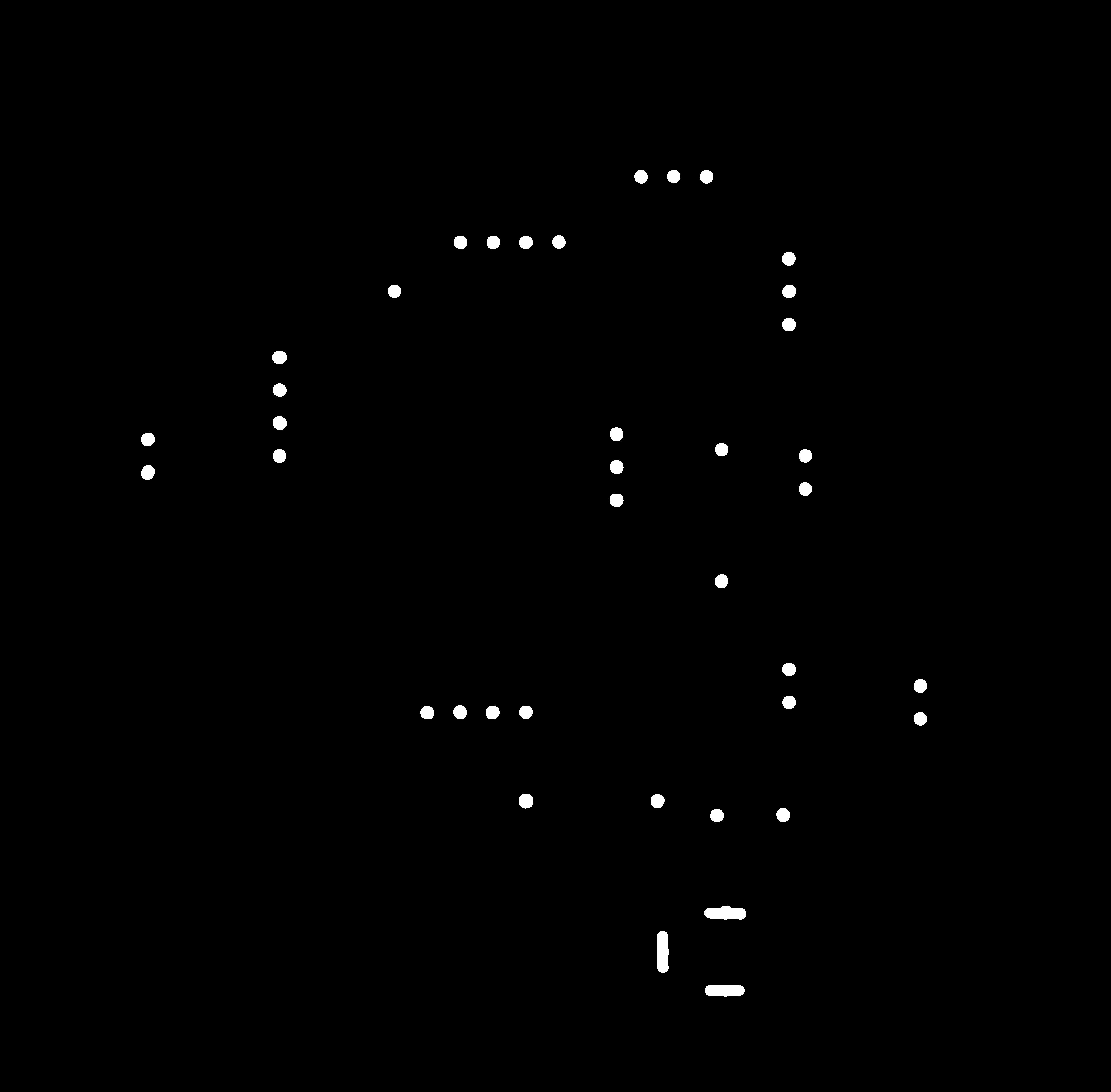
Holes for through holes components , please dont forget to invert the the image befor making .rml file
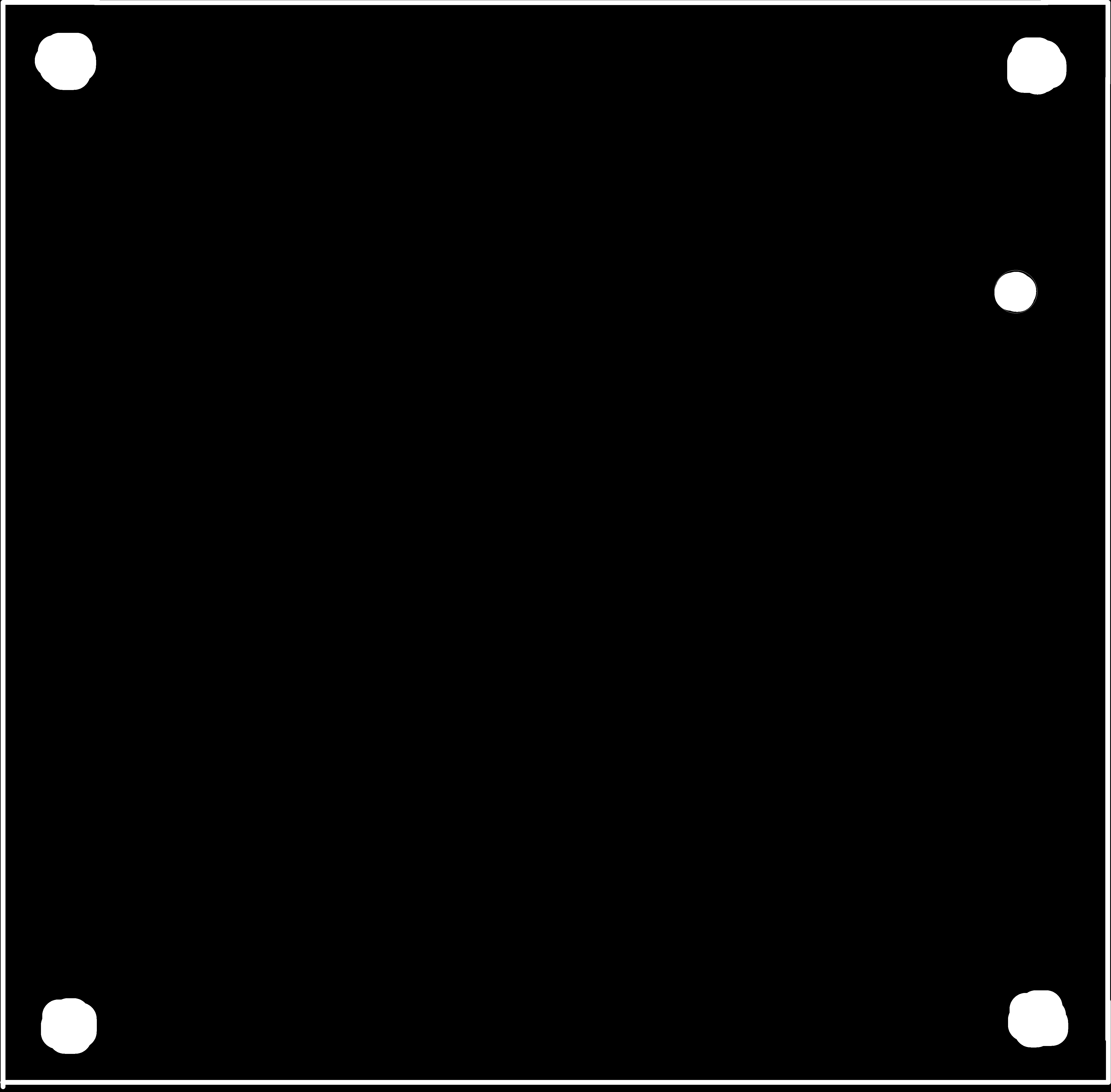
This is for border or you can say cutout part
Timeleapse video for pcb milling
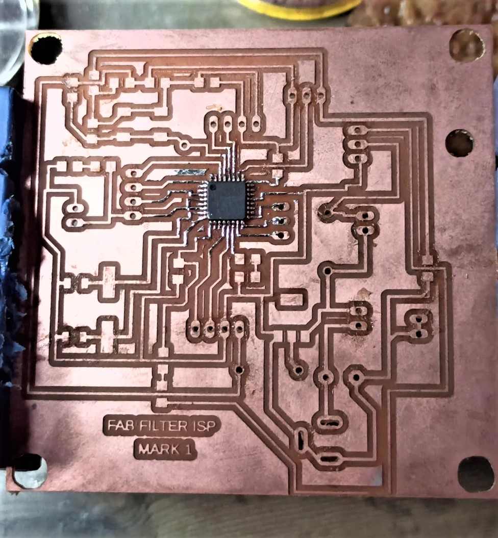
Finally got a pcb
Time to start soldering
A important word of advice make a list of components required for you pcb and take them our and marked them in line , it will save a lot of time an keep the working pace
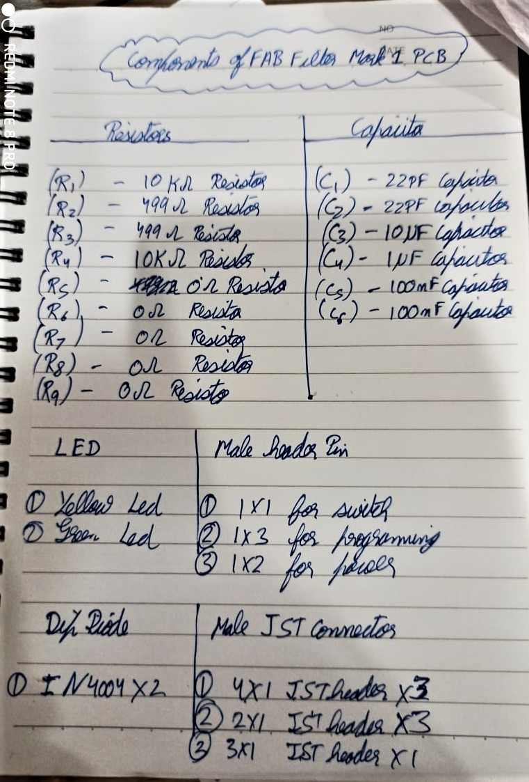
Like i said brought ought all the components according to my list and then start soldering them in the same manner
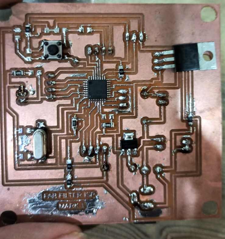
This is partially soldered pcb
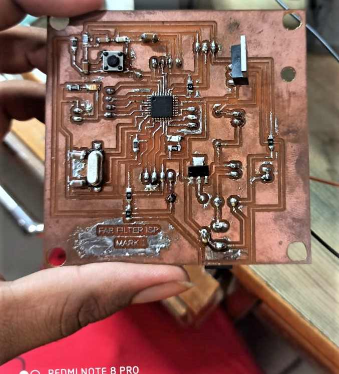
This is fully soldered PCB , and i dont understand why when i finished soldering all the components my PCB looks like crap
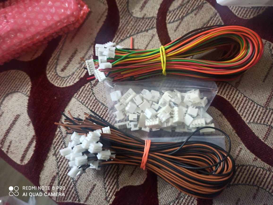
Rather then using the same jumber wires for connection we preferred to go with JST connectors as , you can through this image , and we easily get ther track for eagle ,the main purpose of doing that was to eleminate those loose jumper wire's
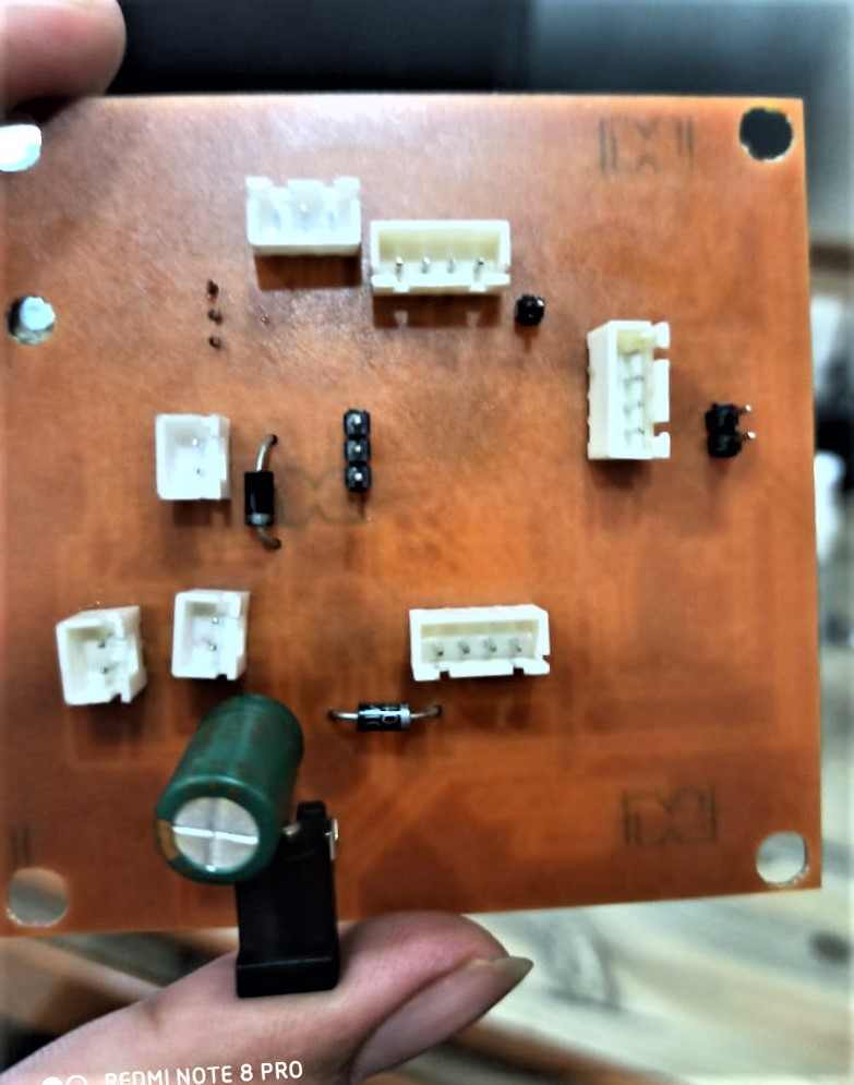
Through this image you can see how we only have those JST connectors only and we preffered that way
If you like to know how iprogram my board pls click on this link , it will guide you to my embedded programing page
Input devices
For this i have used PMS 7003 high effeciency ppm sensor
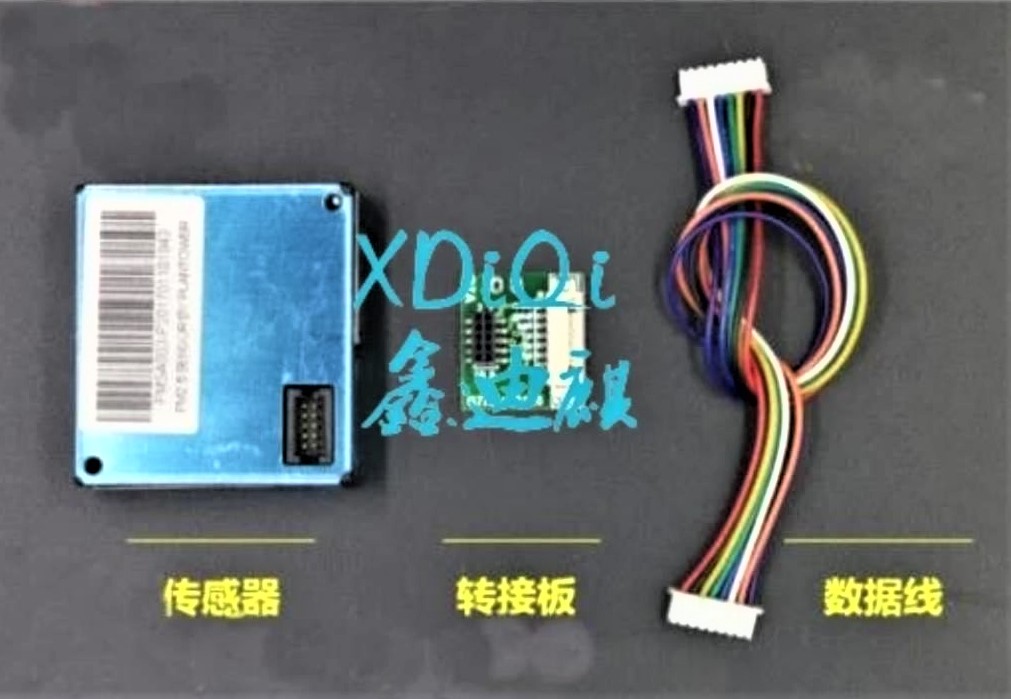
If you woul like to know how i integerated that pls click on this link, this link will guide you to my input devices page there i have in detail explained how you can integerate the sensor , as well as i have provided the appropriate programming