What you will find on this page:
-
What did I learn during the FabAcademy in 2013?
Etching pcb's at home
Milling pcb's in the lab
Vinyl cutting pcb's Soldering pcb's
Programming the ISP
ISP's applied
Hero shot!
Reflection on this week
Manuals and design files
Back in 2013 I learned a lot of useful information about the production of pcb's. In essence, this wasn't hard as I had 0 knowledge about electronics back then, even until the day of today, my knowledge of electronics is far less as what I wish it would be. This seems to be one of the topics where it's very hard for me to remember and understand what is happening. The same level of mastering as you've seen in the past weeks won't be reached here, but I'll do my best to explain everything in case there is another person on this globe in the same position as me. Or as we sometimes state it: if you can explain it (to kids), you understand the matter.
The FabAcademy in 2013
So what exactly did I learn back in 2013?
- Interpret a image of a pbc as posted on the FabAcademy site
- Mill out a pcb
- Soldering
- Soldering a pcb with smd components
- specifics about pcb's (e.g. copper plates, washing them...)
- programming the ISP
- What is an ISP?
During the FabAcademy 2013 cycle, I produced every pcb on the Roland Modela. In the case of the ISP, the code is on the class archive and only needs to be downloaded and send to the machine. I don't remember that much about what I did back then, and my 'manual', well, isn't good. But I do remember using 2 bits and having to take out some hashtags to change the code depending on what I wanted to do: mill out the actual traces, or mill out the pcb itself.
Another new thing that I learned then was soldering. My site from 2013 mentions that I learned soldering in school. 6 years later and I don't even remember that. Whenever people ask me
when and how I learned to solder, I refer back to this moment during the FabAcademy 2013 cycle. We're 6 years later now and the mistakes I made back then! Soldering pcb's or just thin wires
is completely different. What I do remember very vividly was that after soldering for some time, my head started to hurt. Later, by joining the lab where I work now, I learned that when soldering
(for long periods of time), you best have an air suction that takes out all the poisonous gasses. We didn't have this back then. Lesson learned!
I also found it very interesting to solder small SMD components. You needed a very steady hand learn how to work with the soldering iron, tweezers, tin and much more. I'm still intrigued
by it until the day of today. Not sure why, but I find it very fascinating how you can put so much 'brain- and power' in such a small component.
On the part of programming the ISP, I'm still in the dark. I don't think I ever understood what exactly I did when programming the ISP or what my commando's ment. It just worked and I was happy with that. Back then... I'm not in 2019.
When I'm telling at work that I'm making an ISP the are looking weird at me. A programmer, I repeat. But that's how far my knowledge goes about an ISP... Guess this will be an interesting week in the FabAcademy 2019 cycle.
As proof from 2013: have some pictures!
ps. I love how chaotic my soldering was back then
To top
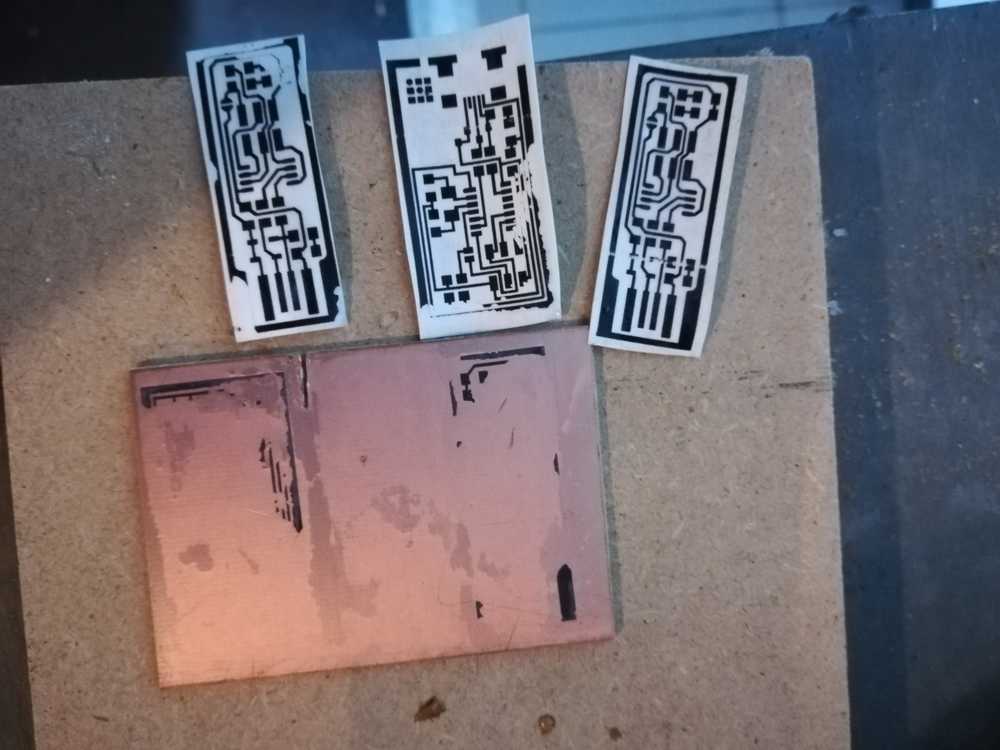
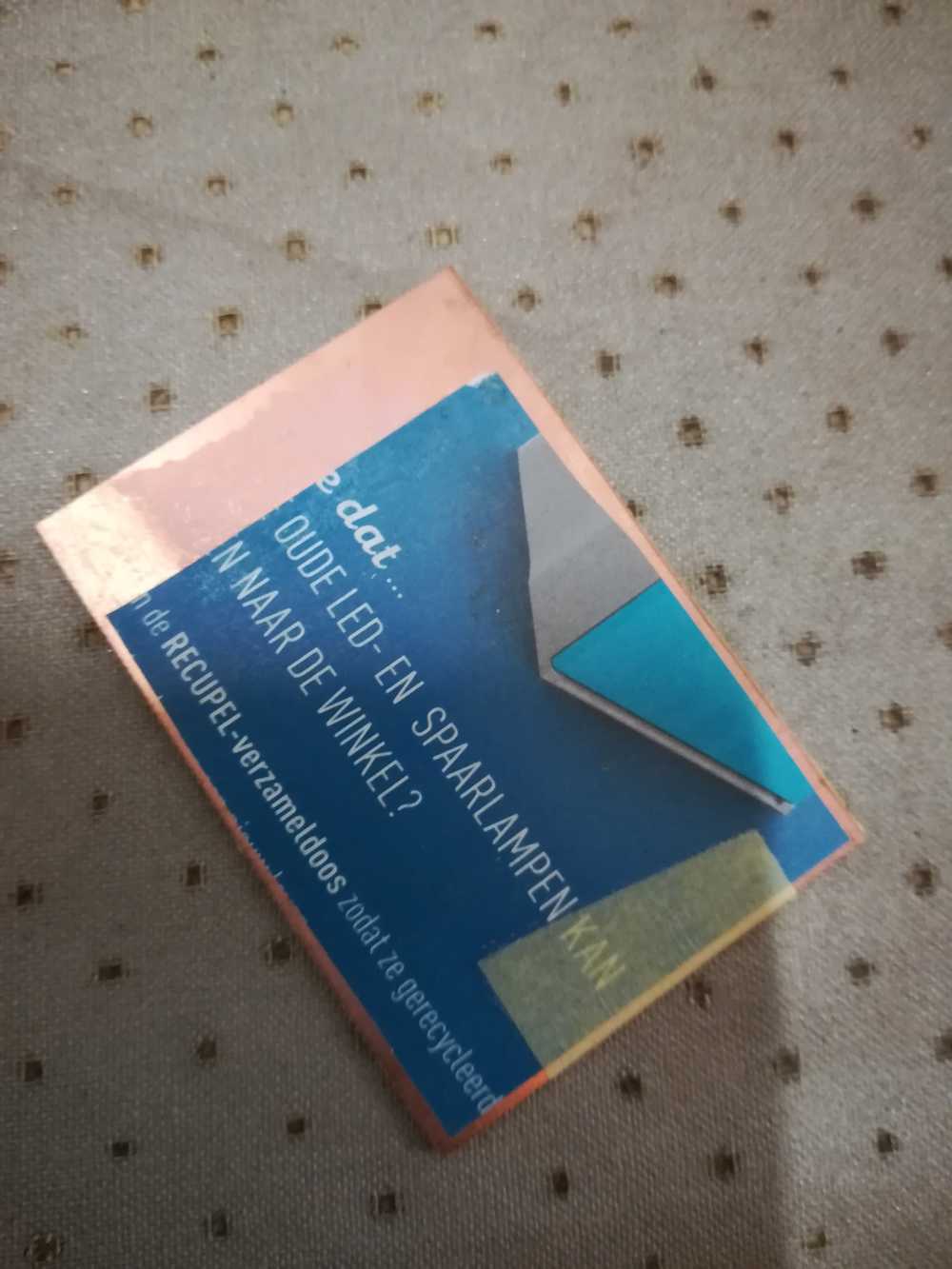
Etching pcb's at home
The etching of pcb's within a lab is 'forbidden' due to the work with chemicals. But I don't have a lot of possibilities to go to the lab in Brussels outside of the class hours. As my
projects still need to be finished, I'll be prototyping the pcb's at home, and mill the final pcb out in the lab in Brussels.
For this I'm using the tutorial that Victor made last year. I started with finding my
way though a dozen of tutorials online on how to etch pcb's. Sometimes the chemicals change (mostly 2 chemicals are used) but the reaction always stayed the same. After talking to
some of the mentors in the ULB lab, I learned that with ferric-chloride alone you should be good. Heating up the substance or adding oxiginated water will only speed up the process.
Once I gathered all the components I started etching. Here you can find my workflow.
- Step 1: Collect all the necessary materials that you will need.
- Ferric chloride
- Cups, pots... to etch in. In my case I uses old Nutella bottles
- Gloves
- Glossy paper (photopaper in my case.
- Laser paper printer
- Circuit printed on the glossy paper with a laser printer
- Ironer
- wooden plank (or ironboard)
- Copper plate
- Tweezers
- Camera to document your process (or phone)
- Paper (to clean up when you spill...)
- Little saw
- Baking paper
- Step 2: if you haven't done this, print out the circuit on glossy paper.
- Step 3: Iron the print to the copper plate
- Step 4: wash the paper off
- Step 5: start etching
- Step 6: rinse it off
Be sure to print on the right side of the paper. Notice which side is up, or put a small cross on one of the sides. In my case, the glossy side needed to be down.
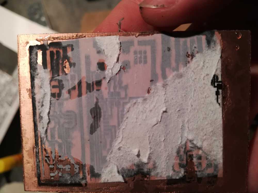
I did this several times and every time I got a different reaction. But here is what I learned: be careful when applying the ironer for the first time, If you layers shift, so does the whole layout of the pcb. One of my best prints (with sprayglue) got ruined that way. I always used baking paper in between my print and the ironer to keep the ironer free from glue residue.
A small mention about glue. I ended up using 3 methods. In the first tries I used stick glue (similar to pritt). In the second test I used spray glue. My third test resulted in me using wood glue and in my last time I skipped the step of glue. The restults: the cheap version of Pritt is a water solvant glue. So the moment it got into contact with water, bye bye adhesion. The spray glue was awesome, but made the layer shift, and left a small layer over the ink so that I cannot etch. Woodglue was a bit better than the cheap Pritt version, but not ideal. The best results were booked without any glue. The glossy paper would detach and leave a small layer over the black lines but that's perfect.
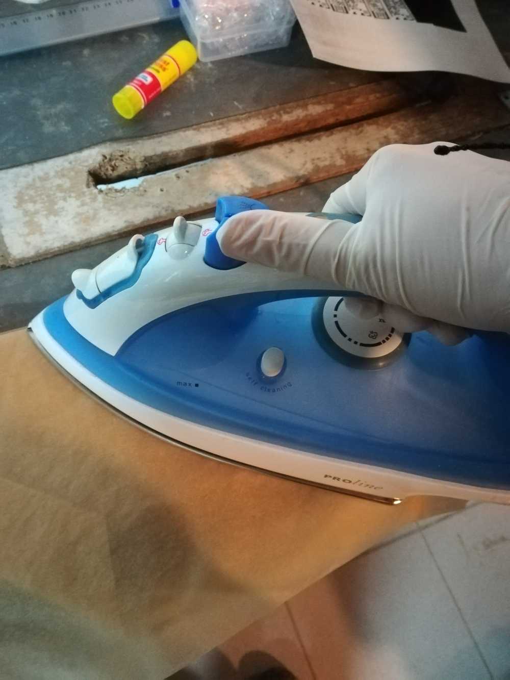
When you think that the ironer has been on the plate long enough, put the pcb in water and wait until the paper comes of. Here to, I ran into some problems. I might have used the ironer for to long. I often had the problem that the paper didn't want to detach. Other problems were that the ink did not attach to the pcb. So I could restart all over. But also that the glue used, left a layer over the whole pcb Scratching it of was no option as that would take away the ink to.
Note: So there is a weird thing with the glue. You don't actually need glue to glue the paper to the printboard. But the heath transfer makes the paint glue to the board. Some things sometimes seem to get lost in translation. To all, it doesn't matter how late it is, or how tired you are: ALWAYS DO CRITICAL THINKING!
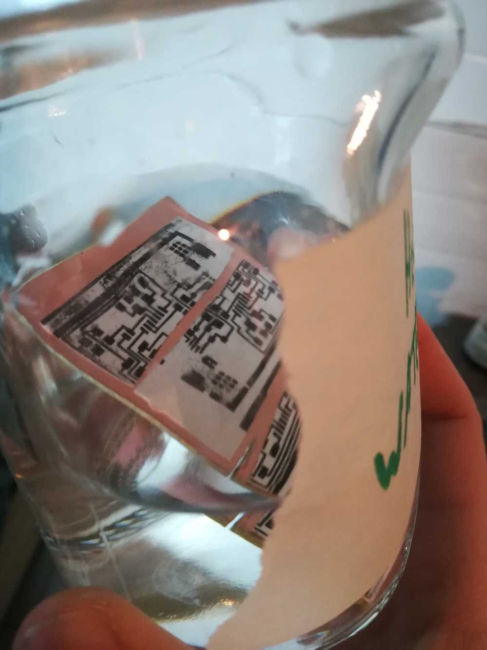
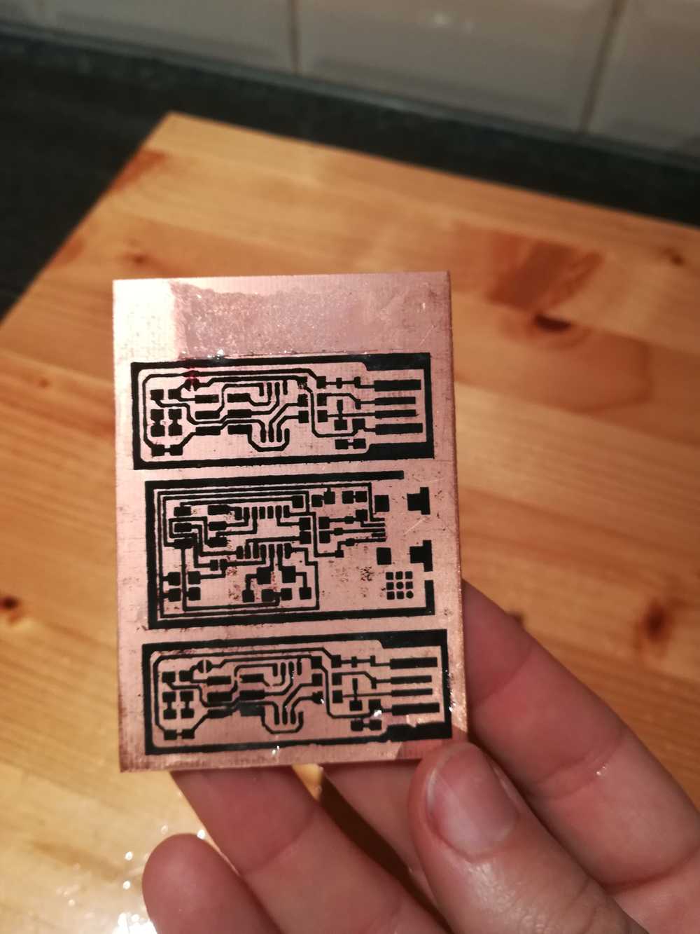
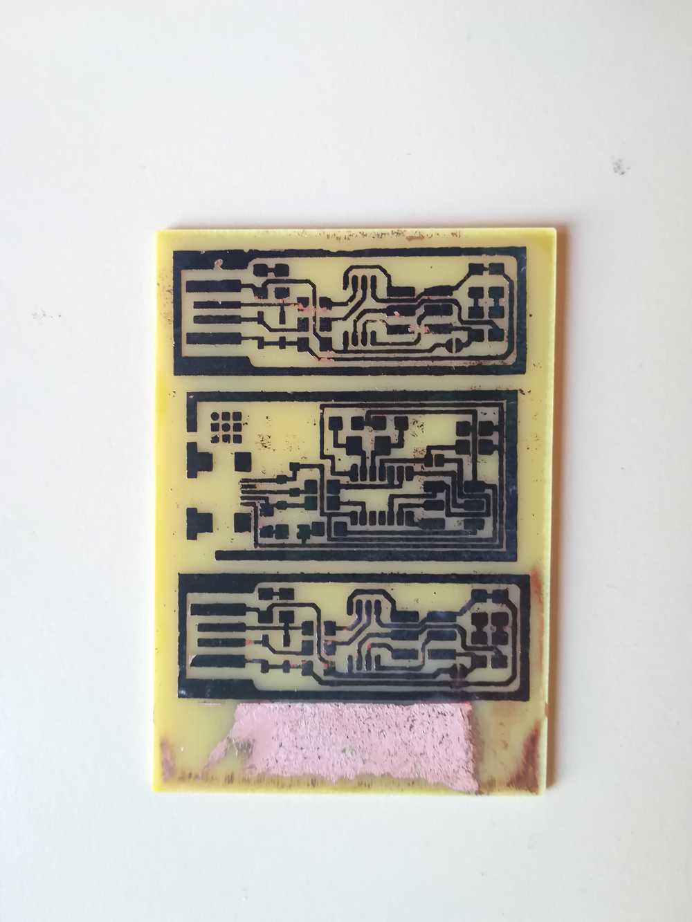
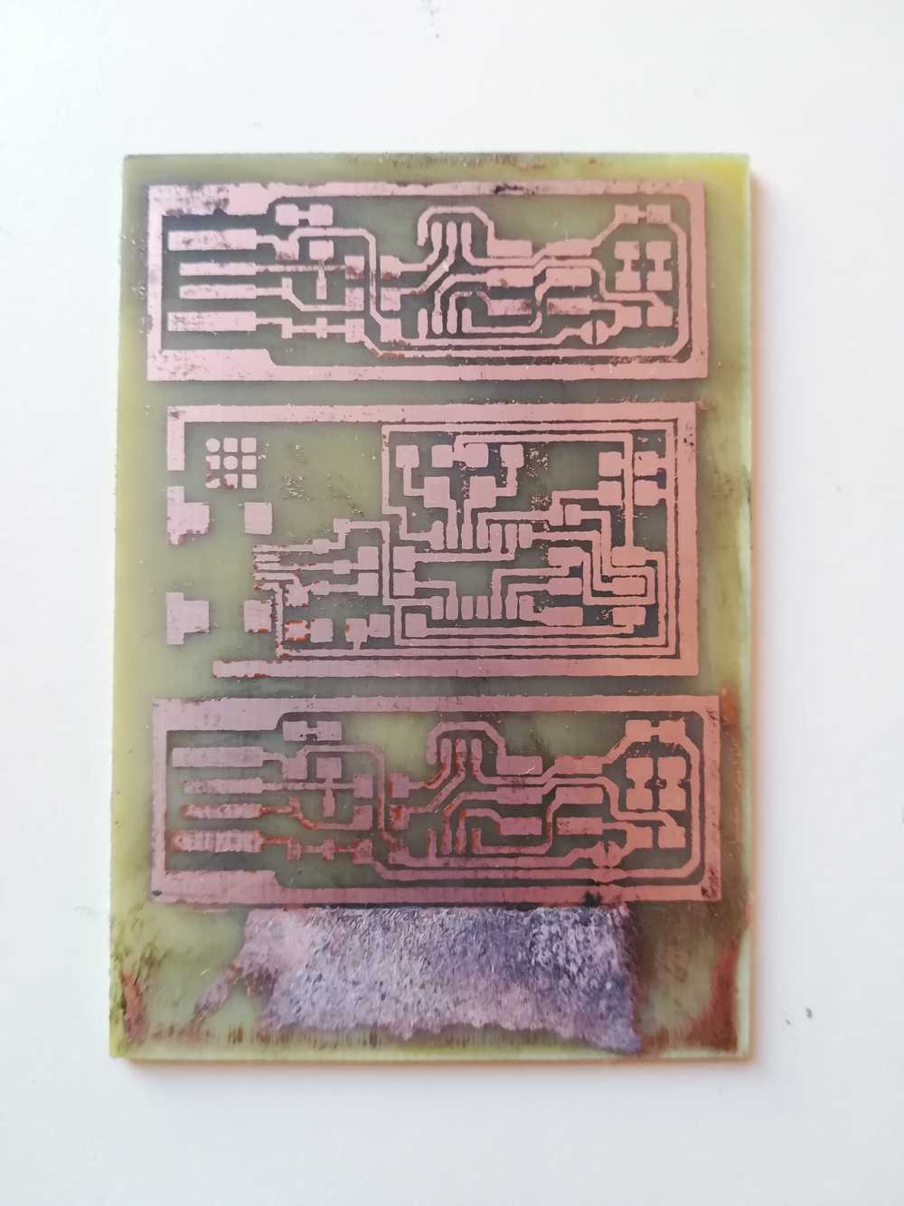
This is the most dangerous step, but also the easiest. Once you peeled off all the paper from you'r pcb, put it gently in the etching solution. Try not to splash the pcb into the container as you don't want to burn your hands (even with gloves) or stain the table. Everything it touches will be yellow afterwards (if only this was the way to make gold and life elixer). Once the print is in the solution, I left it in there for about 15 minutes. Around half way I took a look on how it was going and shook the bowl around a bit.
The last step before you can actually tough your pcb's bare hand is to wash off the ferric-chloride. For this I used the same water that I used to peel off the paper. Once the pcb is clean you can wash off the oil from your fingers with soap and start soldering.
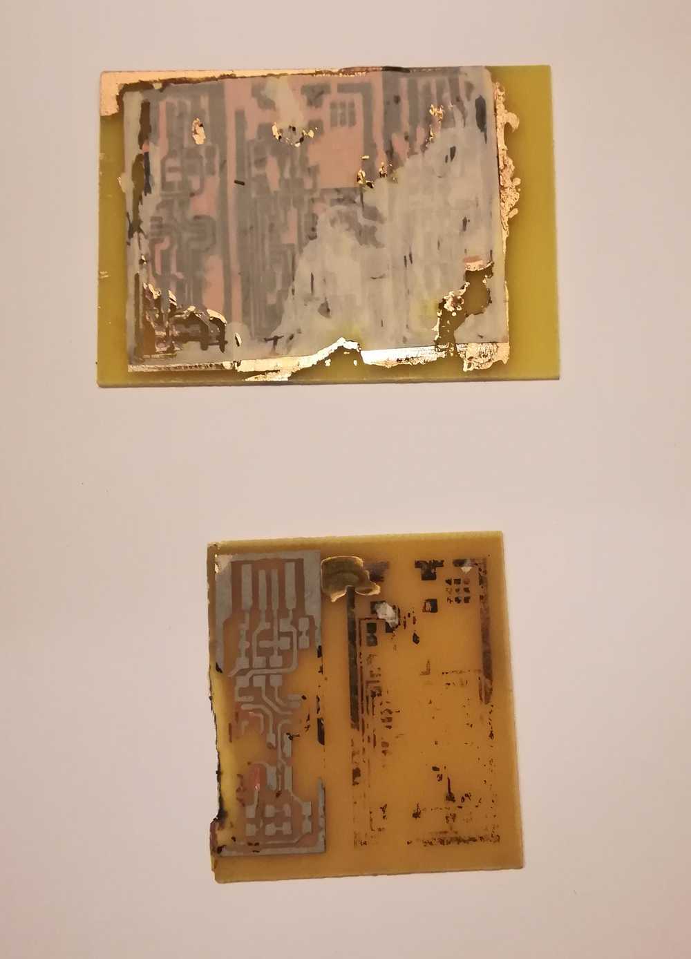
As you can see, I didn't get any good results yet. Solutions to problems are using different paper that its even more glossy and not using the glue. What they ment with it was to use a little bit of scotch to connect the paper to the pcb so that when you iron it, it doesnt move. The added glue like I did, only put another film over the whole pcb and doesn't get etched. As my milling problem for my prototyping pcb's is not solved yet I'll definitely look further into this next week as I already finished 3D printing. It migth be a more dangerous way to produce pcb's but as we have a whole course around etching in our lab (yes, for children) it's interesting to find some good examples for the kids and teach them how pcb's are made.
I tried again and this time I got awesome results in less than 20 minutes. I followed the same steps as above but changed the paper and didn't use glue to fixate the print.
To top
Milling pcb's in the lab (group assignment)
Full documentation on the group assignment can be found here!
On Thursday, the day after class, I was lucky to be able to spend time in the lab for the group assignment. Greta and me arrived early and we decided to take a look at the vinyl cutter and copper tape. We have a cameo 3 in the lab as vinyl cutter. In my own lab, I already did some tests on the Cameo, and they didn't turn out well. We decided to put our brains together and try it again. No success.
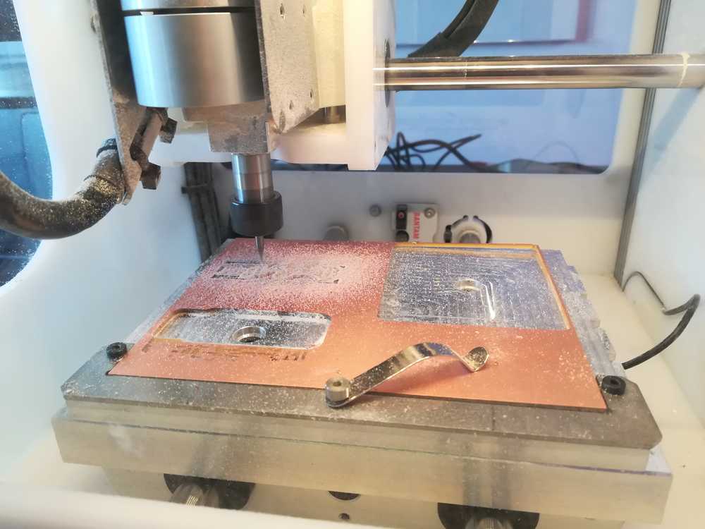
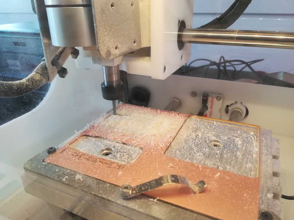
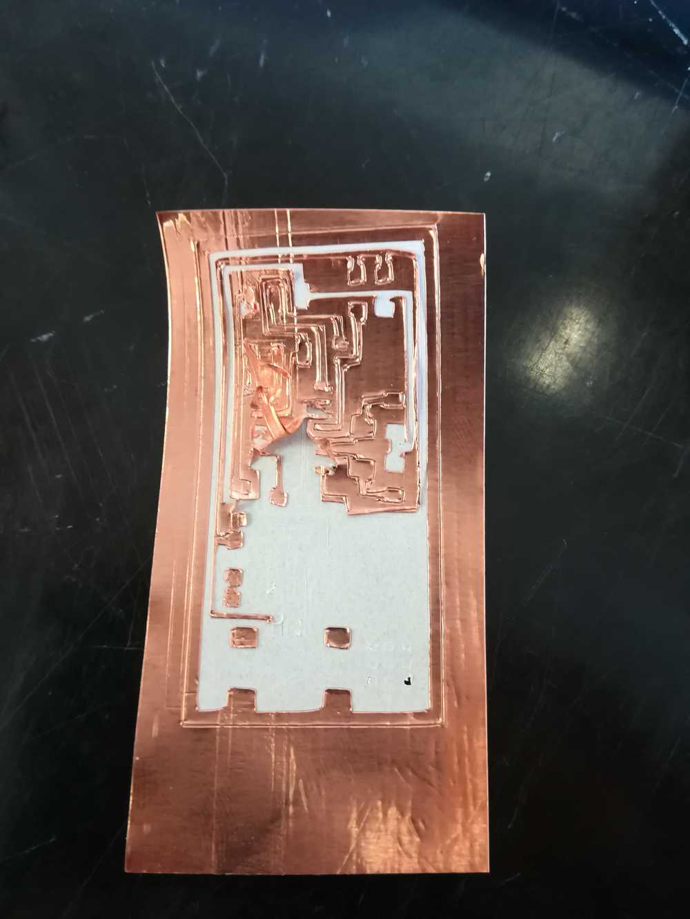
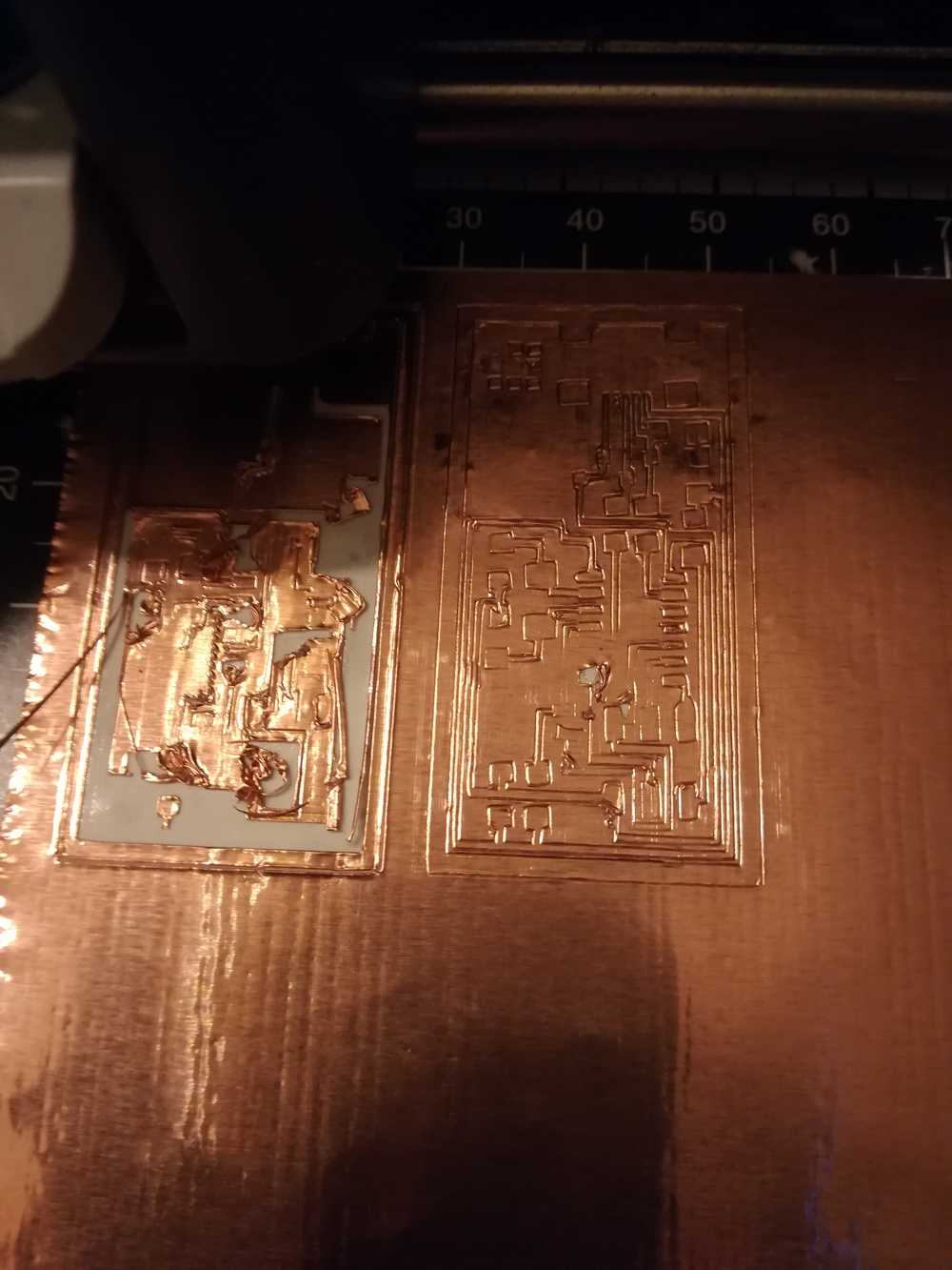
By the time we were done testing the cameo, we started out milling the pcb's on the Bantam machine that we have in the lab.
Process of this part can be found on the group assignment page.
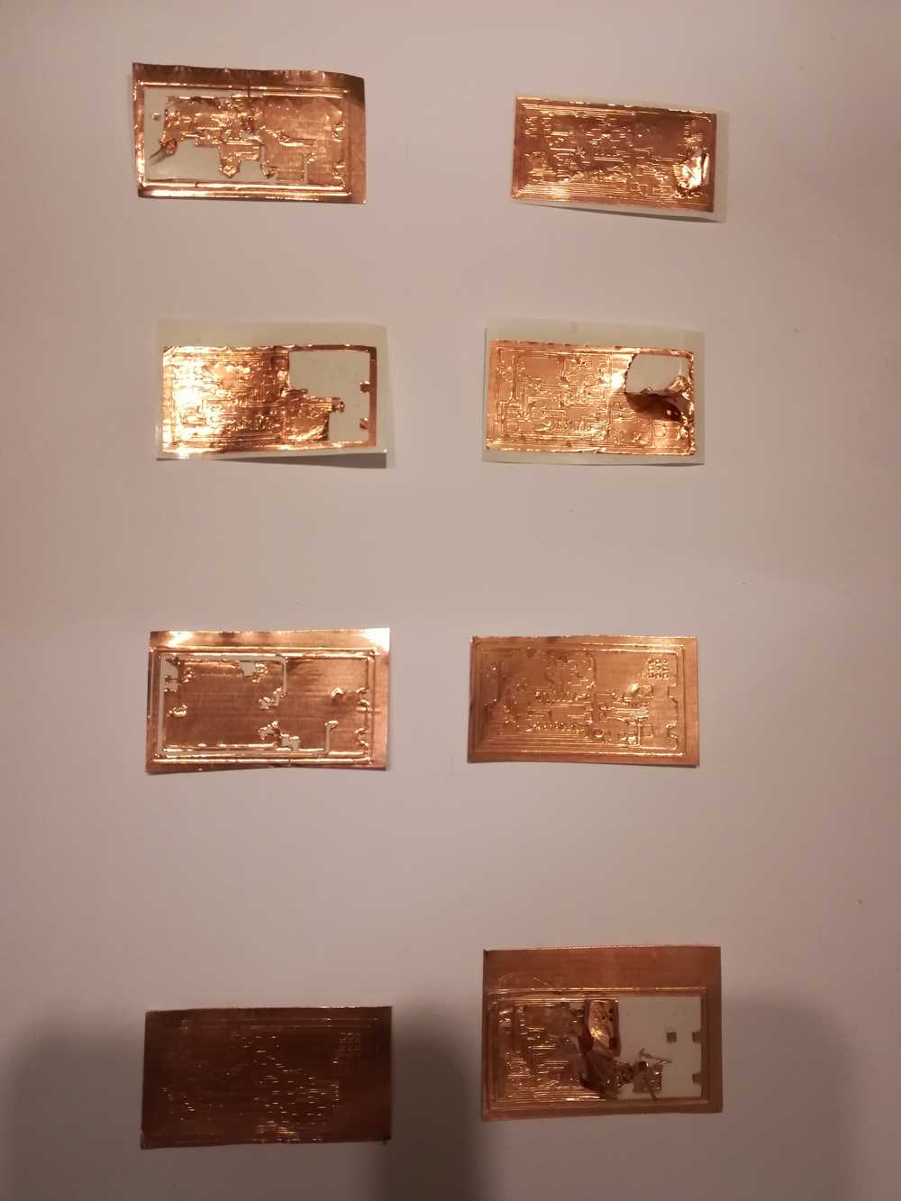
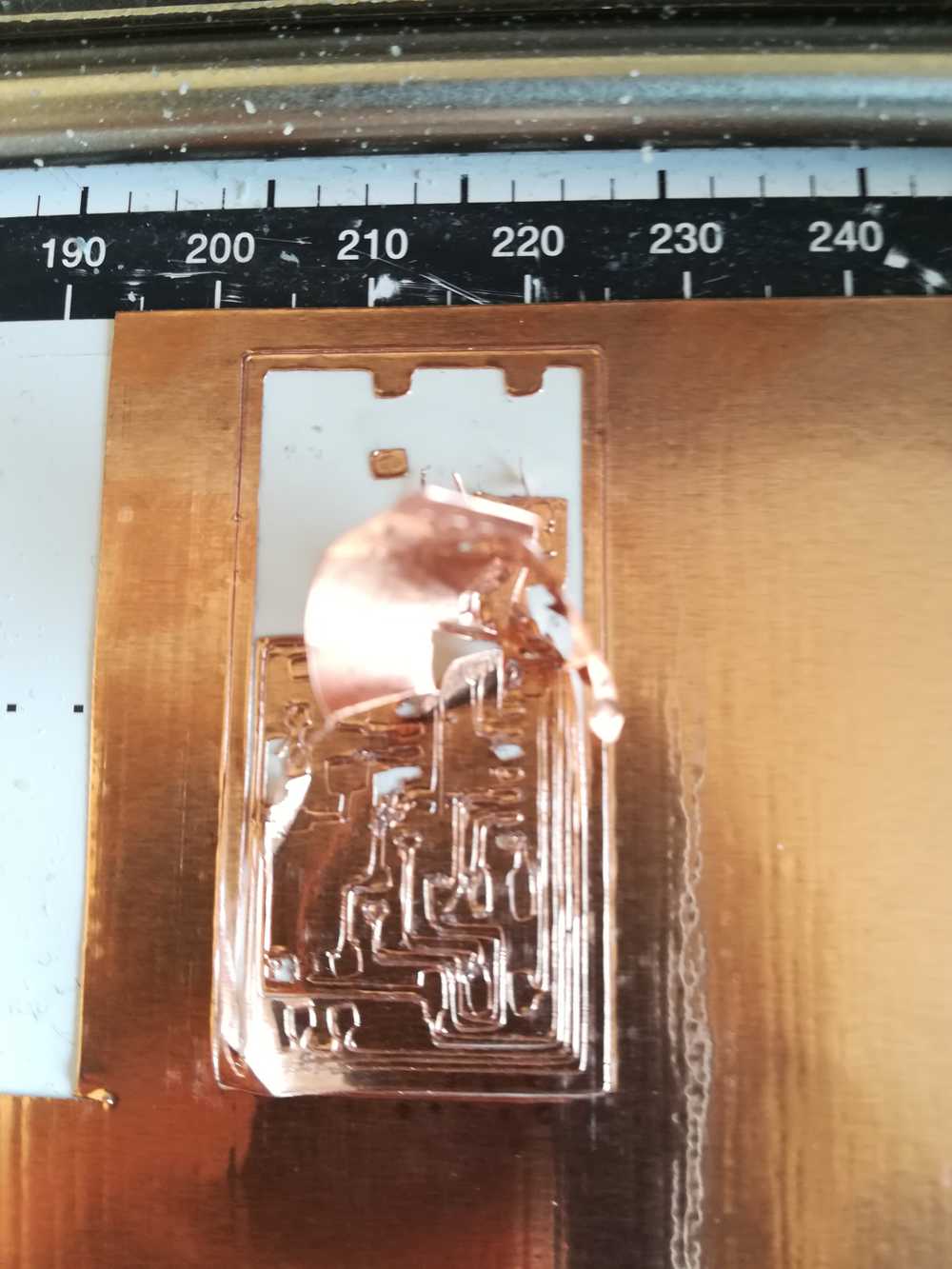
By the end of the day, I got the first fully milled pcb with my home, though there were some mistakes still in it.
I soldered it at home and made some mistakes with the resistors and their numbers. It was however a good exercise in soldering again.
I got lucky and was able to spend another day in the Brussels lab where the guys helped me with milling out a new pcb. I had to ask for help because well, stress can work as a paraliser, and
as my assignment wasn't done by sunday, there was stress. But also because I'm on a full linux laptop and cant run the Bantam Software. But we are inventive and tried another solution: PlayOnLinux.
Luckely the download file from Bantam is a windows .msi file. And it works fine in PlayOnLinux. The reason why I didn't use it was because I didnt find the time yet to solve the mouse problem.
Once the software runs and the machine is connected, both the touchpad and external usb mouse start acting weird (see solution below - added later). But there was not much time, so we made a deal. Windows laptop for milling,
and my linux laptop for flashing the already finished ISP's.
When you are milling with the Bantam machine, you'll need 3 bits. You start with the 1/64, after that, on the same layer (engrave) the 1/32. Last but not least the 1/8 to do the cut out of the pcb.
As I wanted to focus less on milling and more on other techniques, the full plan can be found on our class page: Click me!
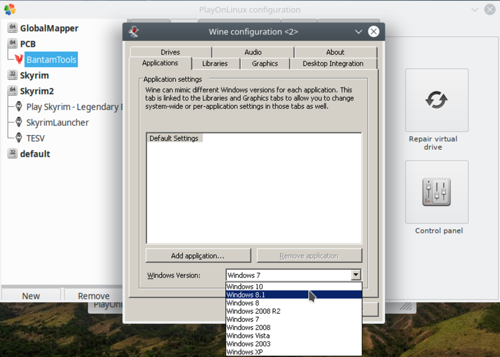
Bantam on Linux
I do want to add a extra topic about running bantam on Linux. In case of some programs, and games, I work with Wine and PlayOnLinux. As I said, the installer from Bantam is a .msi file so should not have given to many problems. It didn't, installation went smooth, but when connecting to the machine, my mouse starting acting weird. I left it for what it was back then as I was getting stressed about finishing up the ISP. Once that stress was taken away I took a look into the PlayOnLinux software and Bantam. I figured out that you can change your windows version on PlayOnLinux. This did the trick. Update: it did not work with changing the windows version, but feel free to keep working on those steps.
Steps can be found here:
- Step 1: open PlayOnLinux
- Step 2: Configure Wine
- Step 3: choose the right OS
Select the right program and go to 'configure'.
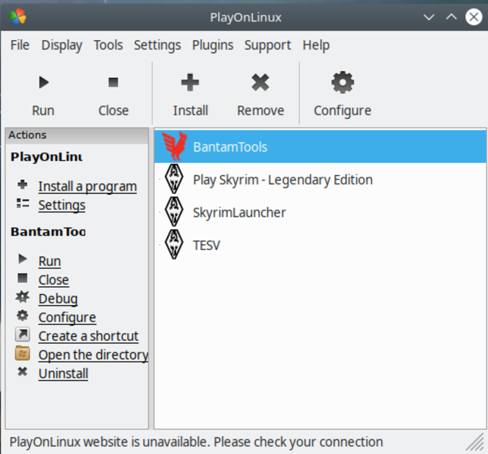
Go to the tab Wine and select the first icon: Configure Wine
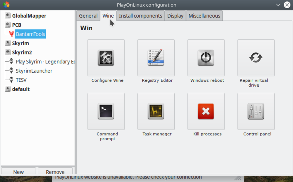
They are quite well updated, and even Windows 10 is already in it. Select one and test out with the machine if you get better mouse results.
To top
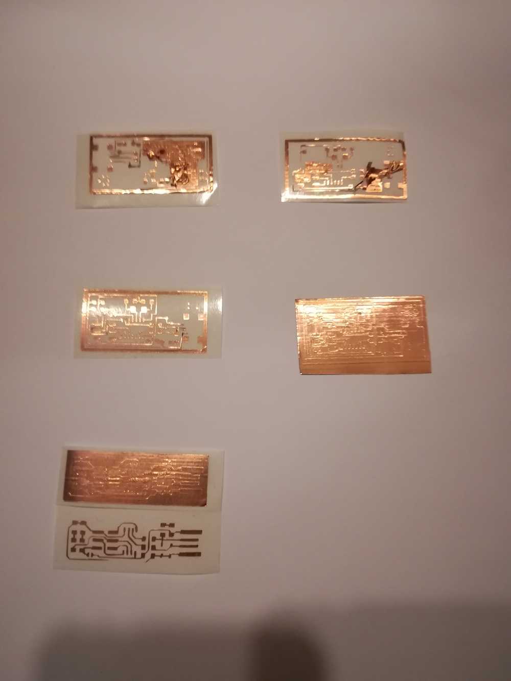
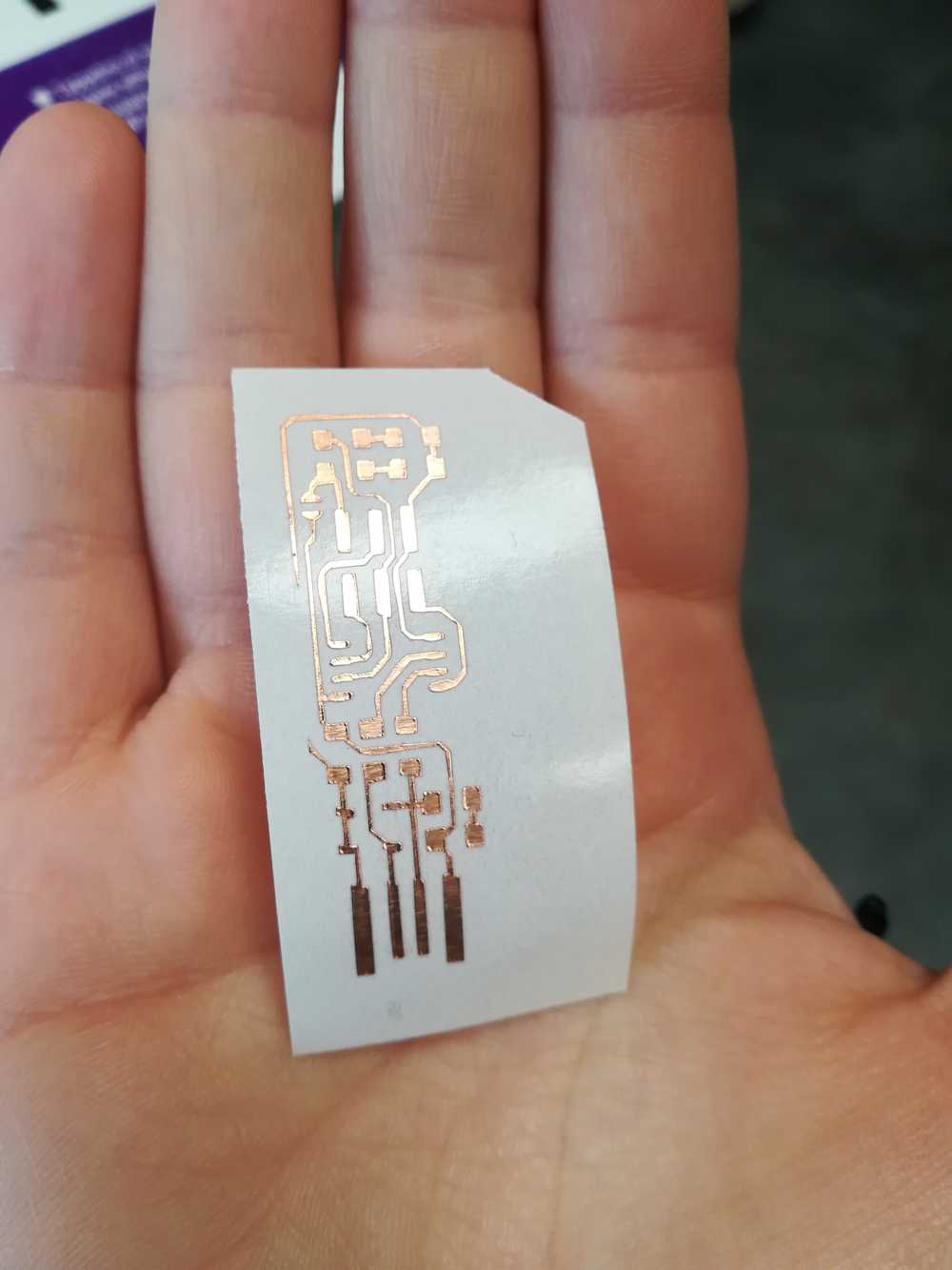
Vinylcutting PCB's
I already started with this in the Computer controlled cutting week. But logically went deeper in to this during this week as I want to use this during my final project. You might remember that in that week I started looking at the settings of the Brother Scan 'n Cut 900 and DX1200 and Cameo 3. During this week I took the testing further with actual numbers.
The Cameo
On Thursday we used the morning to figure out how we could cut out pcb's with the Cameo in the lab. The proces of this can be found on our class page. Once at home I took the Brother 900 with me home. I tested out several settings (there is nothing to find on the internet about this)
The Brother Scan 'n Cut 900
As this is my favorite machine within the range of vinyl cutters (yes, it's not the latest one and does not have 'that many functions'), it has never failed me unlike the more advanced and complicated machines. I took the machine home over the weekend and started testing. Sadly without any result. Often, the knife would just tear apart the copper. And taking the traced with it that we actually need. So first thing I did on Monday was taking out the other Brother that we have in the lab.
| Knife | Speed | Pressure | |
| Test 1 | 3 | 3 | 0 |
| Test 2 | 2 | 1 | 0 |
| Test 3 | 2 | 1 | 1 |
| Test 4 | 2 | 1 | 2 |
| Test 5 | 3 | 1 | 2 |
| Test 6 | 2 | 1 | 2 |
| Test 7 | 1 | 1 | 3 |
| Test 8 | 2 | 1 | 4 |
The Brother Scan 'n Cut DX1200
Everyone in the lab preferes this machine while I don't want to know anything of it. Everytime I've used it, it failed me both on software and mechanical design. But last week I did manage
to cut pcb's with this machine. Sadly not the right size. Time for a second chance. I put in the copper material into the machine and used the automatic settings. It went puuuurfect.
I took a look into the machine and found the next settings:
- knife: automatic
- pressure: 4
- speed: 3
- halfcut: on
 Next time I'm taking out the Brother 900 I'm testing with those settings. The knife will probably be a 2 or 3, mostly 2 as that gave the best cutout results without tearing the material.
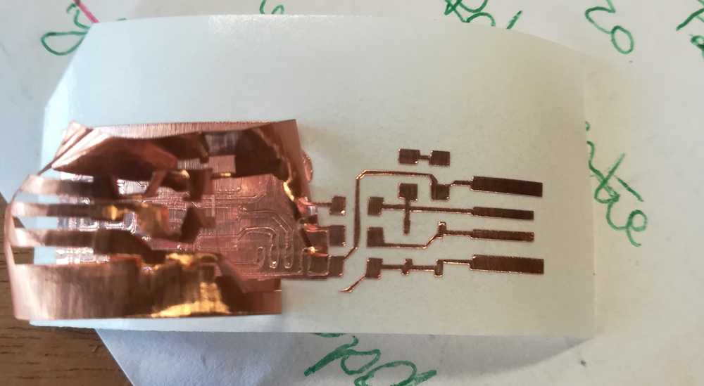
Another problem with the vinyl is peeling everything off. A lot of pcb's have small lines that disappear within the cutting. So we often have to add some ourselves. After a few tries I figured out the best way to peel of pcb's. In the case of Neil's pcb, start with the USB connector side, Once you start having splits, cut them of and follow one trace a time. For Brians' pcb, it's best to start on the opposite side of the USB, once you start having splits, cut them loose and follow one trace a time.
To top
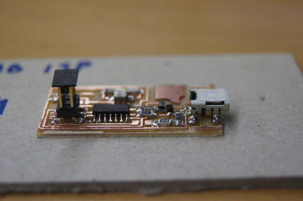
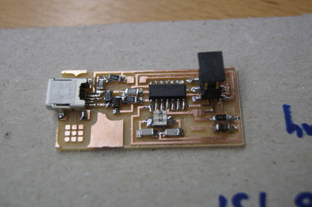
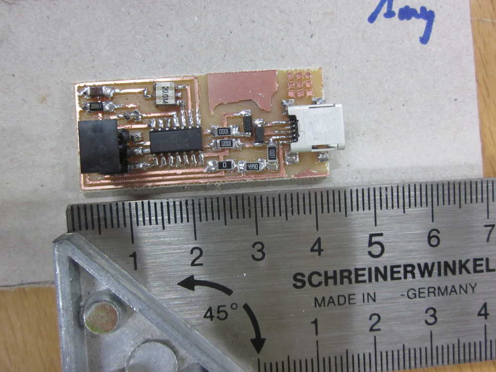
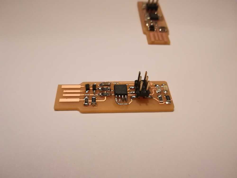
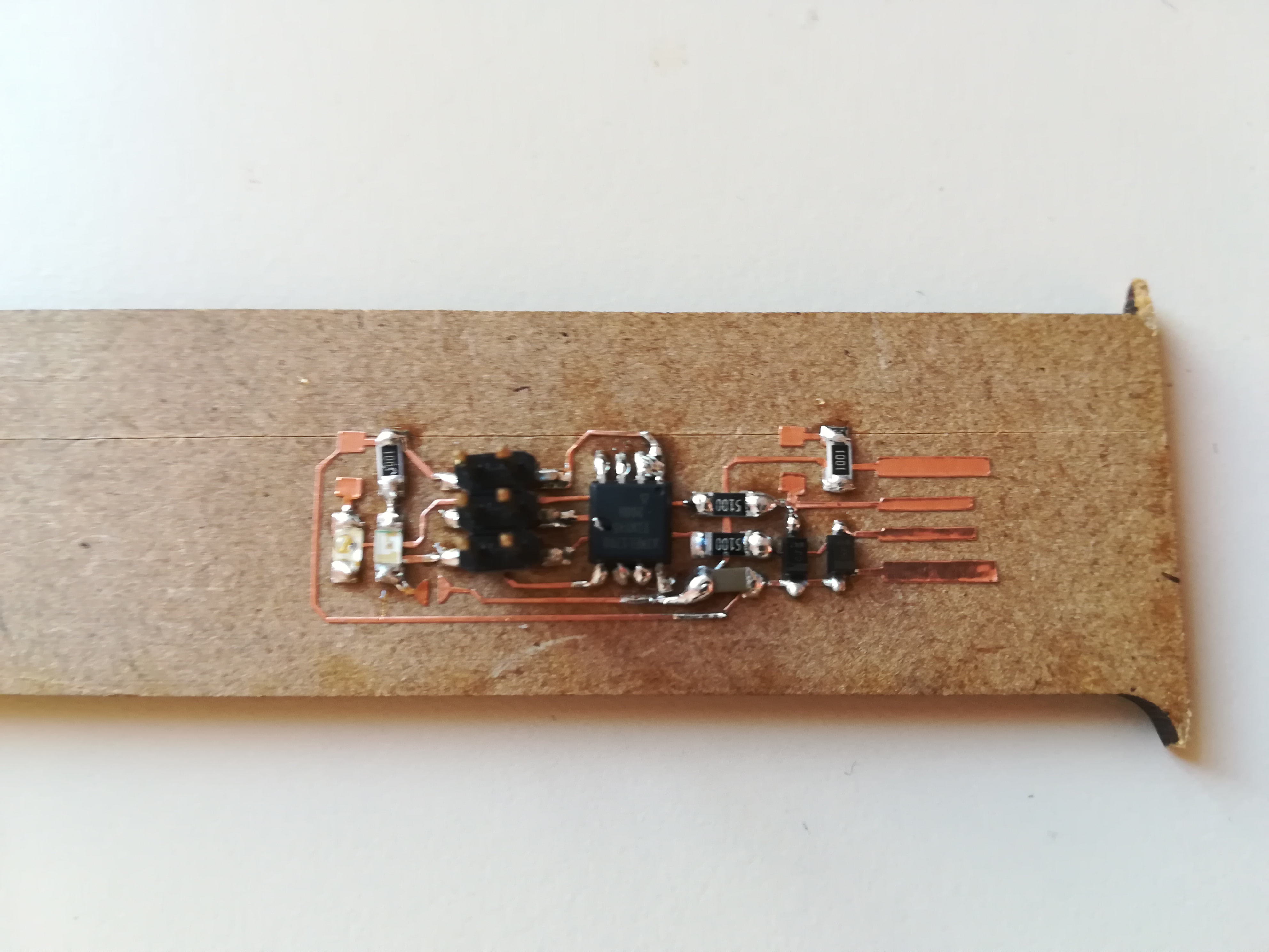
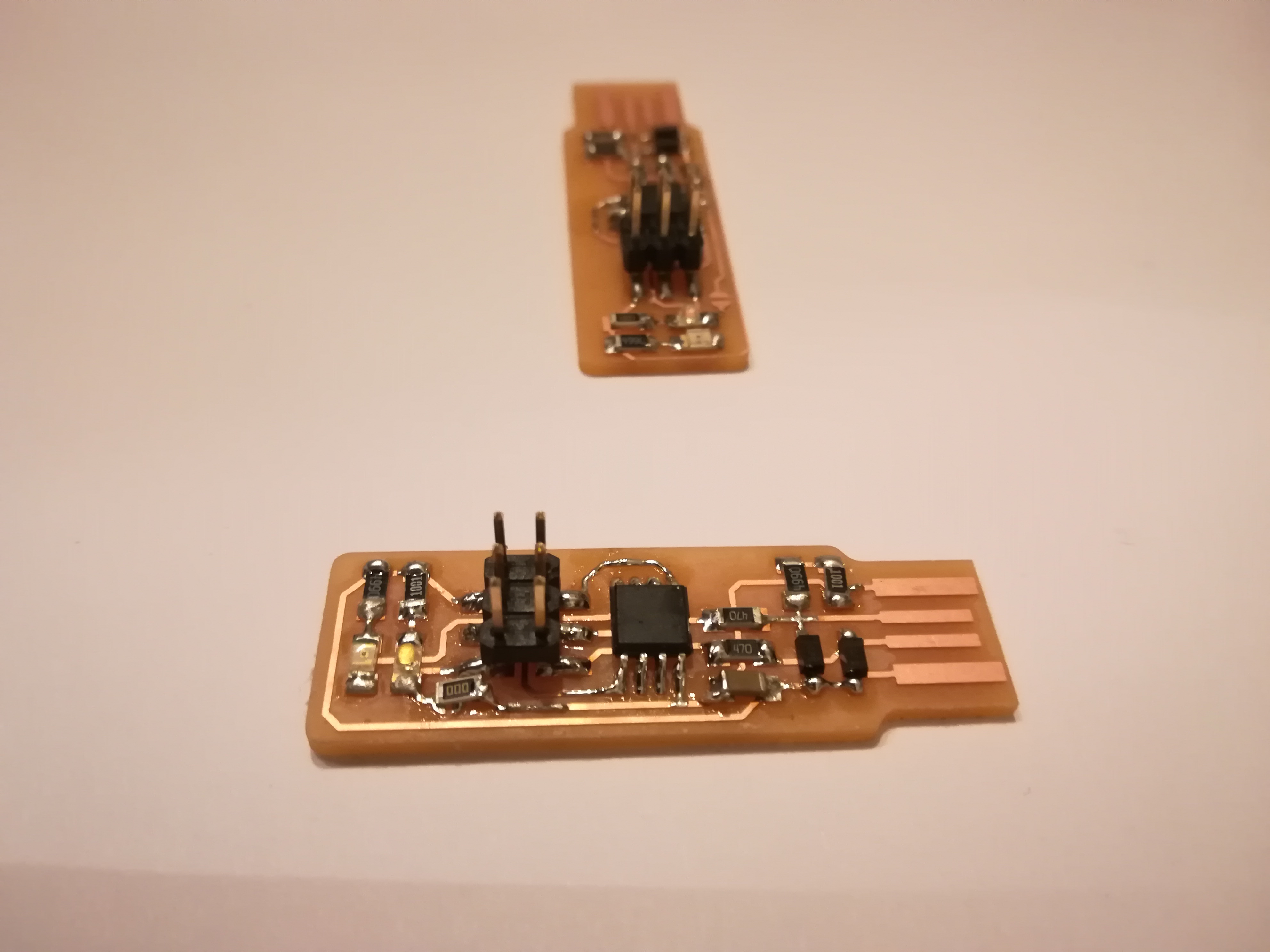
Soldering pcb's
Back in 2013, I learned soldering by soldering my ISP. Sadly, working with kids doesn't require such a fine motoric reactions. I started with soldering the micro controller, but ran into
my first problem very fast. I soldered 2 pins together. I solved it by using another condutive wire to desolder the pins. It took a while as I didn't find the braid. It's
not the way to do it, but it works. While soldering the other components, I didn't really run into trouble. I did use the tips from Neil to sometimes add some tin to the board and only
fixate the component later on.
A fear that I had when soldering in 2013, was that I was afraid of burning my fingers. Sometimes, if you keep the soldering iron to long on the wire, it gets hot. I didn't have that
problem now. Let's keep it to the fact that I got faster at soldering.
List of components and their function
- micro controller: this is the 'computer chip', the brain of your ISP, the memory of it
- LED: light emitting diode is a semiconductor light source that emits light when current flows through it. Or a small light.
- Zener diode: is a particular type of diode that, unlike a normal one, allows current to flow not only from its anode to its cathode, but also in the reverse direction, when the Zener voltage is reached. The Zener voltage is the amount that needs to pass to be able to turn the direction around. See it as a glass of water that only empties when full.
- Diode: semiconductor device with two terminals, typically allowing the flow of current in one direction only. Most known diode is a LED.
- resistors: A resistor is a passive two-terminal electrical component that implements electrical resistance as a circuit element.
- capacitor: passive two-terminal electronic component that stores electrical energy in an electric field.
- pinheader: connects the cables to another board and passes data
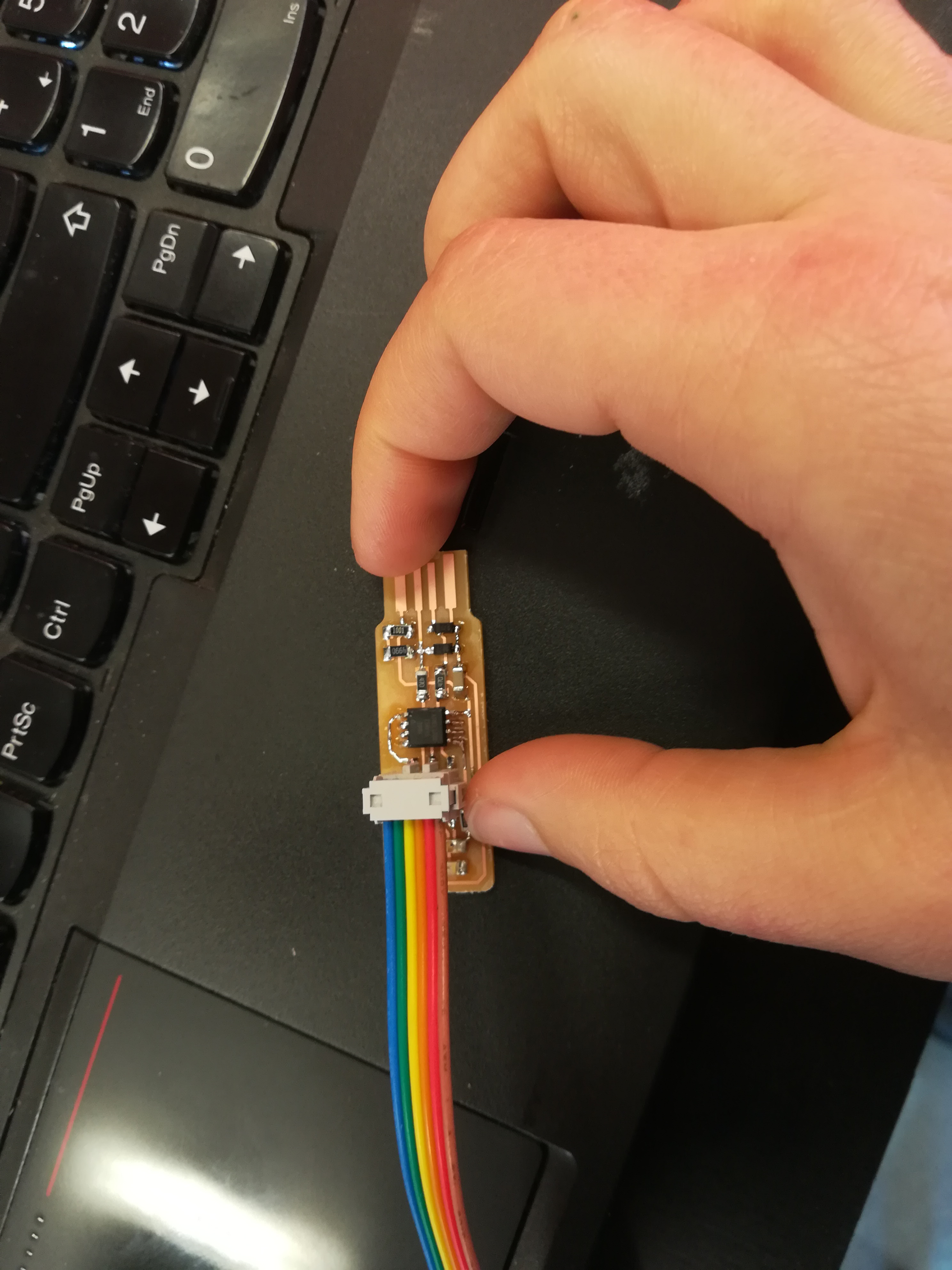
Programming the ISP
As I spend a lot of time in making the electronics, we're nothing with this week if we don't also program the ISP. On my website from 2013 I put some code that works. Well, in theory. This is kinda logical, as you can't do anything if the components are not well connected to your board. Within this I count testing the board with a multimeter. We didn't do this
this week, we just plugged in the ISP into a UBS cable and when the lights worked and there was no smoke we were happy. Well, here starts a tricky part. For this I used the documentation from Brian. I downloaded the file here (get and build
the firmware). After that I needed to install some packages but ran into the error that it didn't know one of the libraries. I solved it by doing "sudo apt install avrdude gcc-avr" without the
libraries, and added them later to the files. In the file are also interesting comands that you'll use now and later on. This can be done with micro controller boards from the Arduino series, or with another ISP. Be sure that you connect the cables in the right order on the header pin. In my case we needed to take
both drawings next to each other and see where GND was, or the other connections Stay in the folder where the .hex is located and type "Make flash" the file will be updated to the microcontroller now Of course, non of it went without problems. One of the first problems was that we didn't know on which USB port the ISP was. The light on the ISP burned, but we couldn't flash. To
see what kind of USB ports you have, type "lsusb" into the terminal. You'll get a list of your connected devices. If you know the name of your device you will see it, if you don't know the
name, do the list twice. Once with the ISP and once without. Also watch out for typing errors! Another problem that we found was that I put on the wrong condensator. The one I had was much much bigger than the one that I needed to use. So we changed it.
For making the .hex file, you need to run the .Makefile in the terminal. Go to (cd Desktop/......) the folder where you unzipped the files that you downloaded,
desktop in my case, and open the file by typing ".Makefile" in the terminal. The file opens and you can create a .hex file. 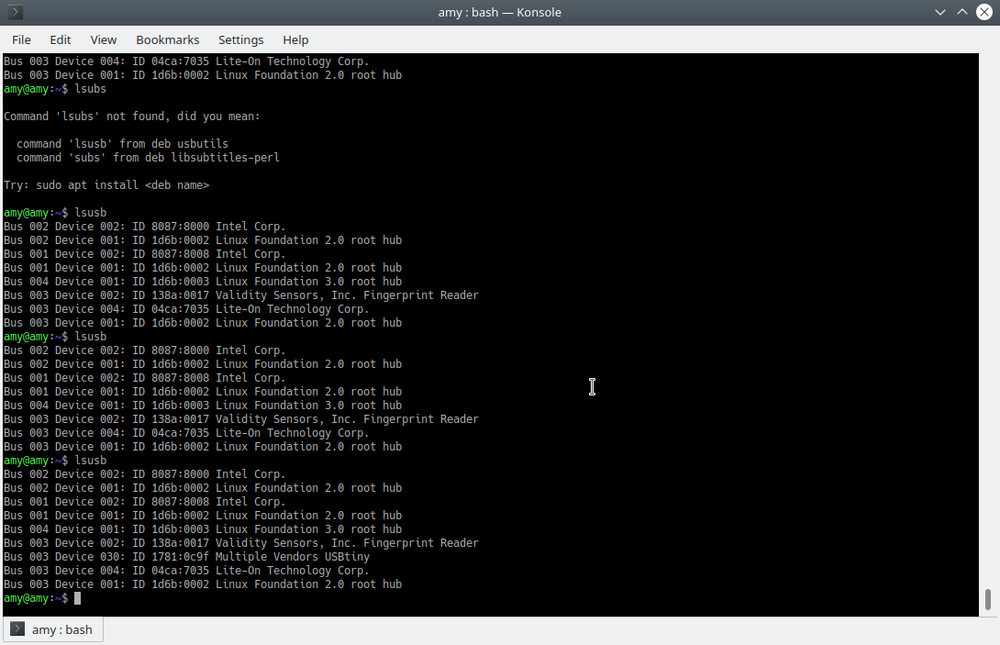
To top
ISP's applied
While I was soldering, my colleagues were teaching the kids how to make flipper machines. As I was in the lab, I didn't escape their questions. They asked me what I was making. "An ISP." I said. "It's a little something that enables you to program other stuff when it's already soldered." The kiddo didn't really understand. So I went searching on the internet and with friends for answers.
I found a little movie on youtube that explained ISP's. Lucky for me, I can apply it directly to one one of our workshops and the second part of my final project.
One of the projects we have in the lab is the Led Up Kidz. We teach kids how to do SMD soldering and pick and place components ( by hand). Next to that we also let them program their own LED blinking program. At the moment we first give them the programming part, load it all up onto their micro controller and start soldering after that. As we all know, soldering sometimes goes wrong and because of that we're not able to adjust the program anymore. An ISP could come in handy for this. And a holder to reprogram them.
To top
Hero shot!

Reflection on this week
All in all it felt like a weird week. Little work to do, not much creativity, I became an aunt and my work wasn't finished by Sunday evening. Something that I try to do for myself so that I do have
Monday and Tuesday to experiment extra but also take the rough edges off my documentation. What comes on the site is often a narrowed down version of what I really did on paper. But I can't
add giant flowcharts every week.
I'm a bit disappointed that I can't make the vinyl work on 2 of my 3 machines. As the machine on which it does work is not trust worthy on performances.
With the Bantam machine I'm a bit annoyed because for now it only works on Windows and I can't find the right solution to make it work on Linux.
Next to that, Sean is my new hero. After class last week I took a look at his giant ISP and it settled down my thoughts for the past weeks. We had exactly the same idea on how to make
giant components, but it's a step forward to for me to see how he connected everything. As my work will be on textile, this is only inspiration.
A thing that I noticed during the soldering and picking the components is that I really need order for the components as my learning disorder hits in with full force. Resistors for example sometimes have a K or an R next to it. To me it doesn't say a thing. It's like x and y and + and -. It means nothing to me. And let's not get started on all the possible ways that I can read 4990. So I was very happy that during the group assignment we made small packages of components so that I could use elimination to find out what component needed to go where.