_week 5
electronics production
What is a PCB and what is a FABISP?
PCB Stands for Printed Circuit Board.
Essentially a PCB is a board that connects electronic components, and they are used in most of the
electronic devices.
The FabISP is an in-circuit programmer (a basic PCB) version of the AVR ISP programmer/board.
During this week's task we had to build a FABISP.
Our model is based on a FABISP revision from another student Brian's, who based his work on Zaerc's FabTinyStar.
The documentation of his work
(which is very clear) was crucial during this week's work.
You can find Brian's documentation step by step HERE.
Group assignment
For the group assignment we had to learn the complete process of doing a PCB, which includes learning and
understanding the following machines and process:
1_How to create the traces and outlines files for the milling machine, using FabModules.
2_How to set up milling machine Roland SRM20 (this machine is only used for the creation of PCB boards
inside our lab).
3_How to solder
4_How to set do the software installation to copy the firmware into our new FABISP.
1_Set-up file for milling machine
We used FabModules to create the .rml extension
file for the milling machine.
This platform what it does is to convert a file into the language the machine "speaks", plus you can set
up all the necessary information to cut the file; such as machine speed, reference for origin, material
thickness, tool diameter and so on.
All the details of how to set up the file in FabModules are below in the individual task.
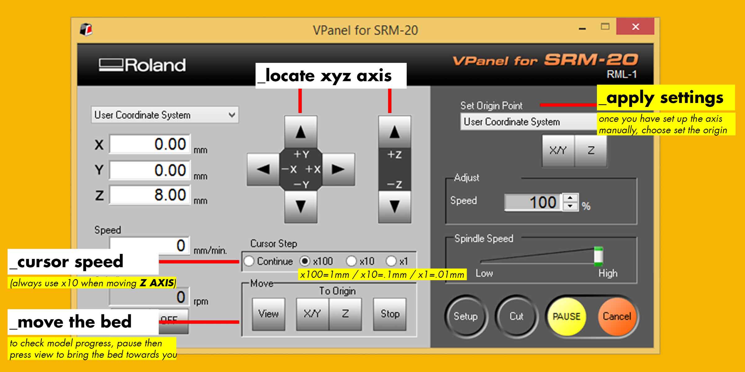
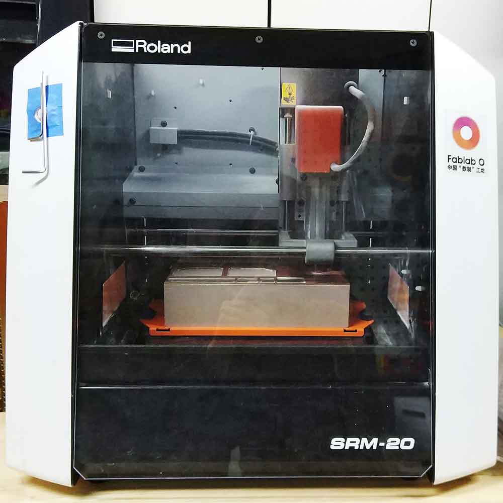
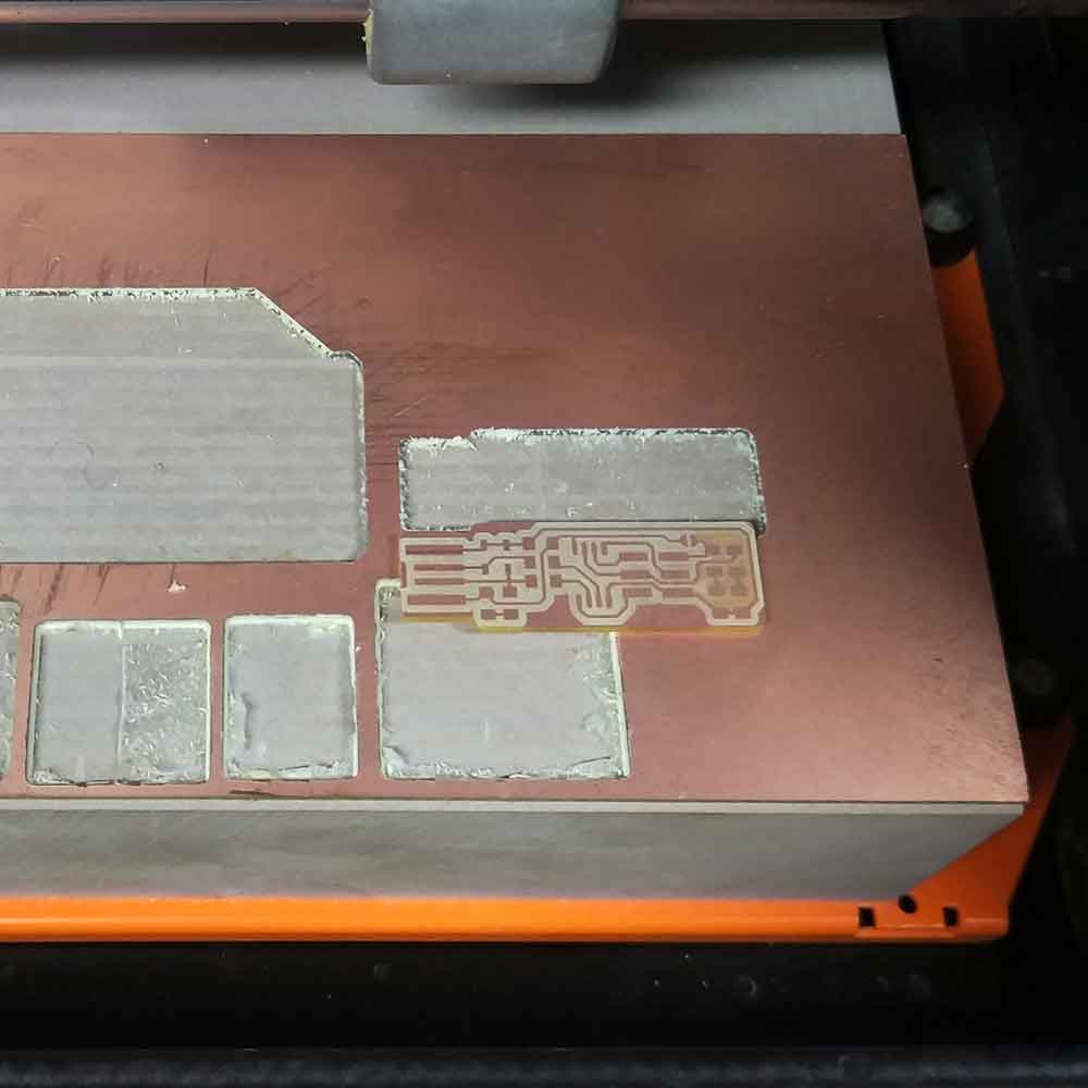
2_Set-up milling machine
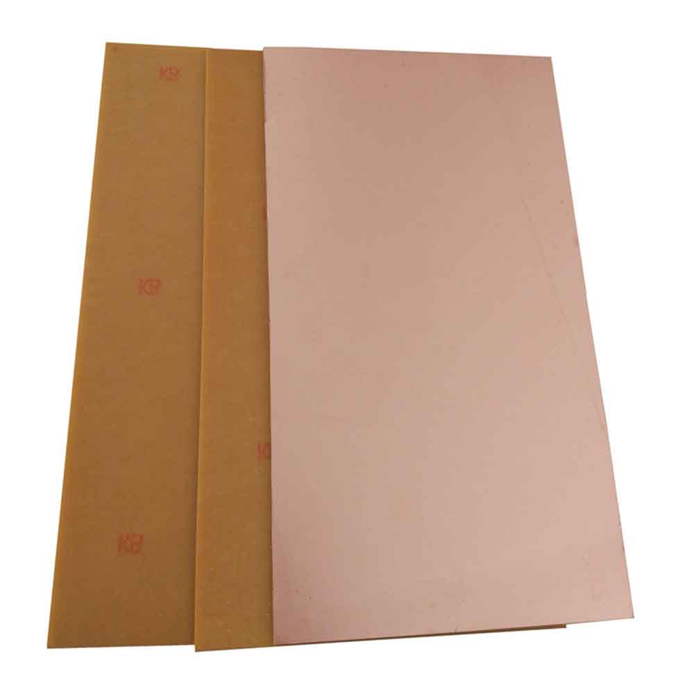
The machine we are using for this task is a small milling machine, a Roland model SRM20, and the
material we used for the PCB is a laminate sheet with a very thin layer of copper (microns of
copper).
A very important part of this process was to understand what drills are the appropiate to use and how to
change them.
In this case we are doing two different tasks, one are the traces (where the machine will remove
material without going through), and the second task are the outline cuts.
The drills we will be using are one of .4mm (only for the traces) and one .8mm only for the outlines
(cuts).
After identifying the appropriate tooling, we learned how to set up the machine positioning.
We began with the traces task (recommended to start with traces than the outline), so we fixed the .4mm
drill beat into the machine. Some advice to add here, you have to be really careful when doing this as
the drill beats tip can break easily.
The first axis to locate is the Z axis, you need to make sure the drill beat touches the material, after
this you have to set the origin for this axis. To do so on the menu go to "set origin point" and press Z
once is located.
After that be careful and move a bit UP the Z axis (you don't want to drag the drill and break the beat
while locating XY axis.
Then locate where you want to begin in XY, know that the reference point (for this machine) is always
the left bottom corner.
After we've set up the positioning, we proceed to select the traces-file:
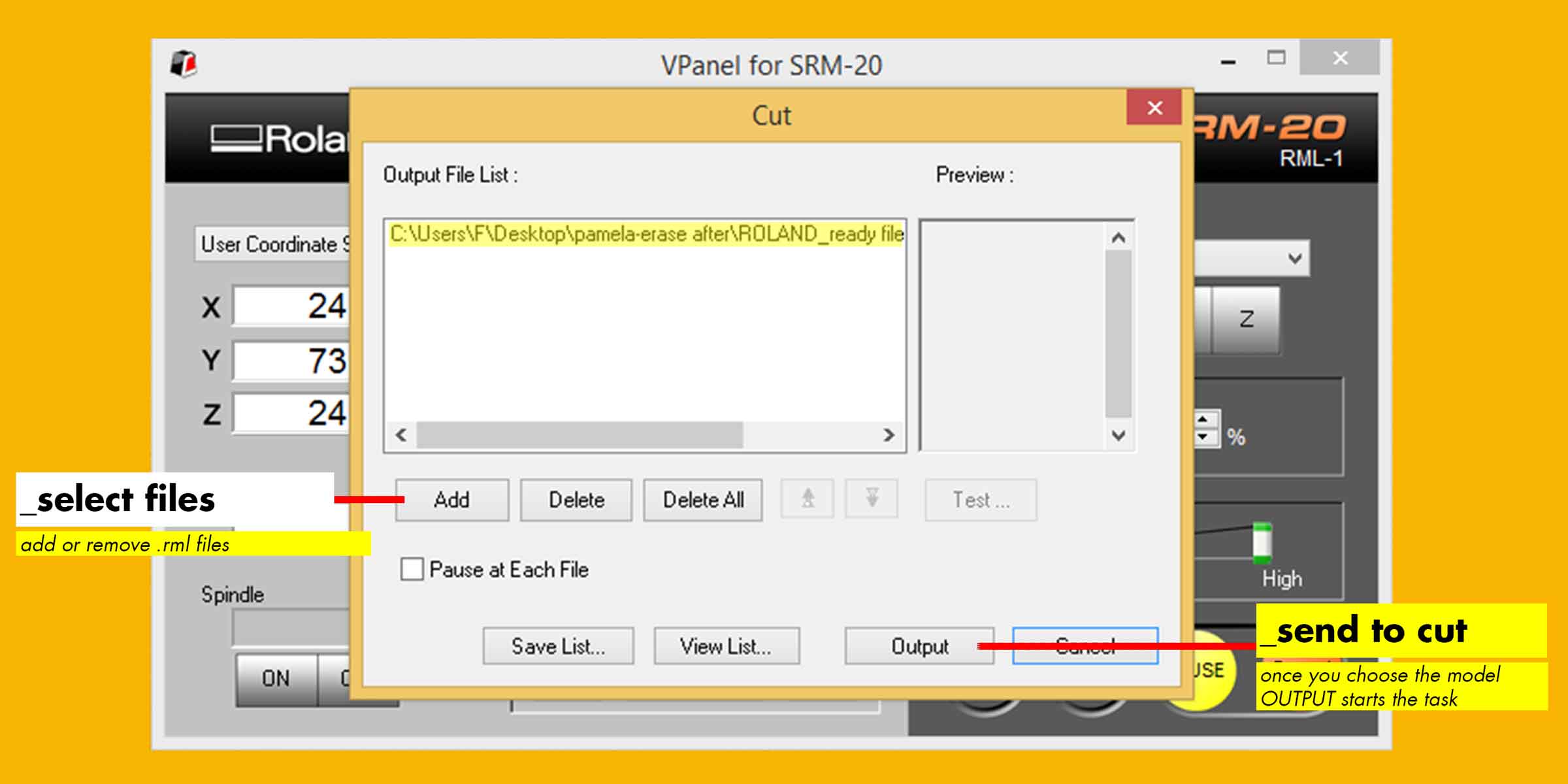
Once this task is done you can send the outlines file, there is no need to set up again XYZ axis as we
already did it at the beginning.
Here are some photos of both process:
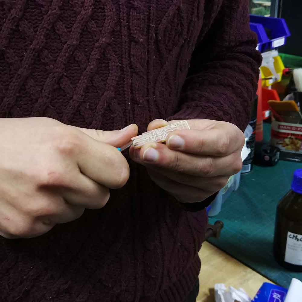
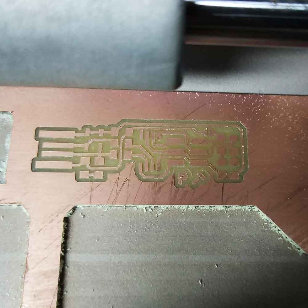
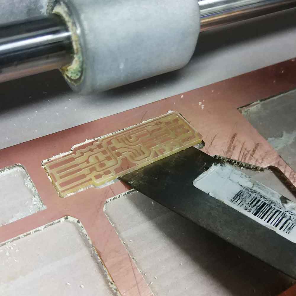
After the PCB is has been cut depending on you settings, there might be some traces of copper leftover on the USB contact, remove them using a knife:
The next part we learnt during the group assignment was how to solder.
The solder we used is a lead
free tin wire.
Soldering needs practice, but some of the things you have to keep always in mind is the order how yous
solder, always begin from the middle and move towards the sides.
If you have tall components leave them at the end or else they will block you while you are soldering
the other components.
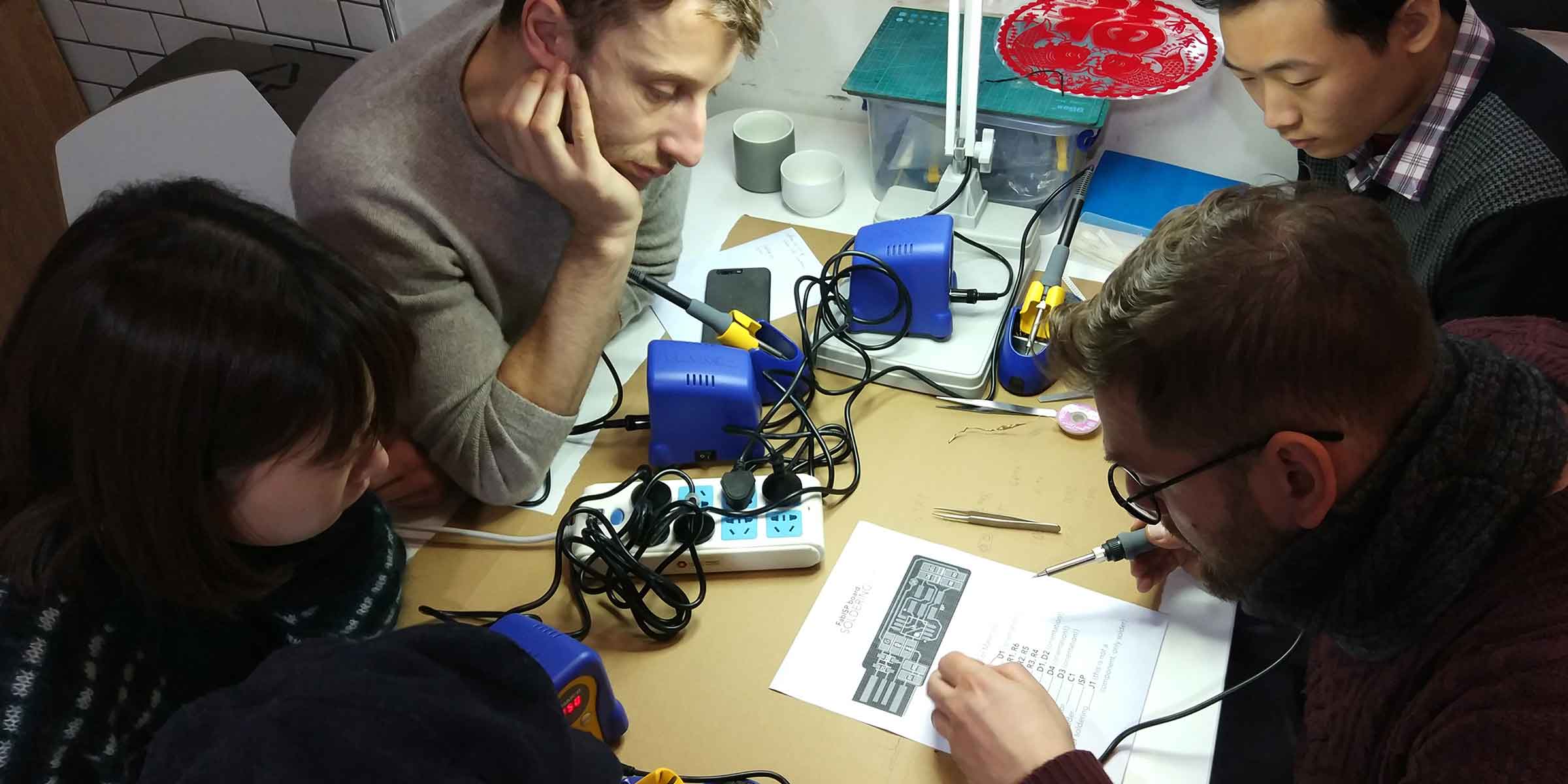
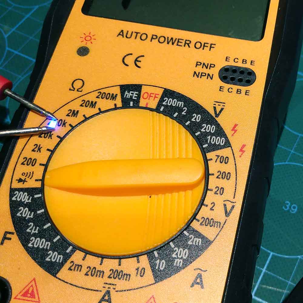
An important and wise thing to do while you are soldering is to check the continuity of the componenets
that are being soldered.
For this we used the "multimeter" to test it:
Individual assignment
For the individual assignment as I mentioned above, we used the model available from another student
(Brian).
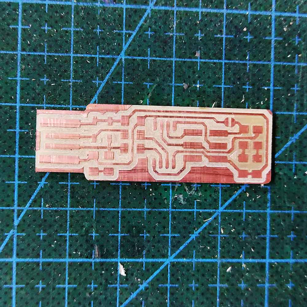
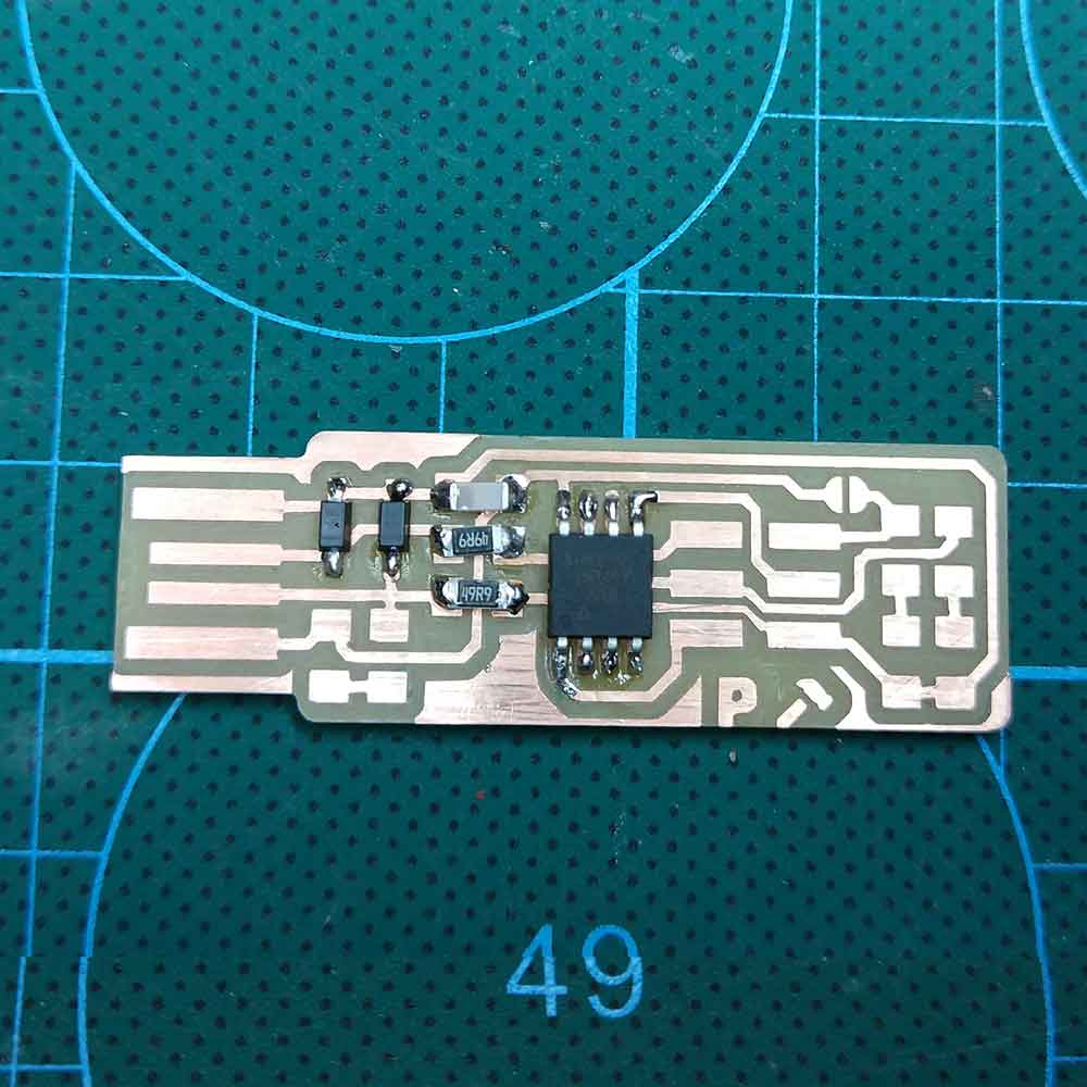
To begin with I downloaded the traces and outline .png files available on his website.
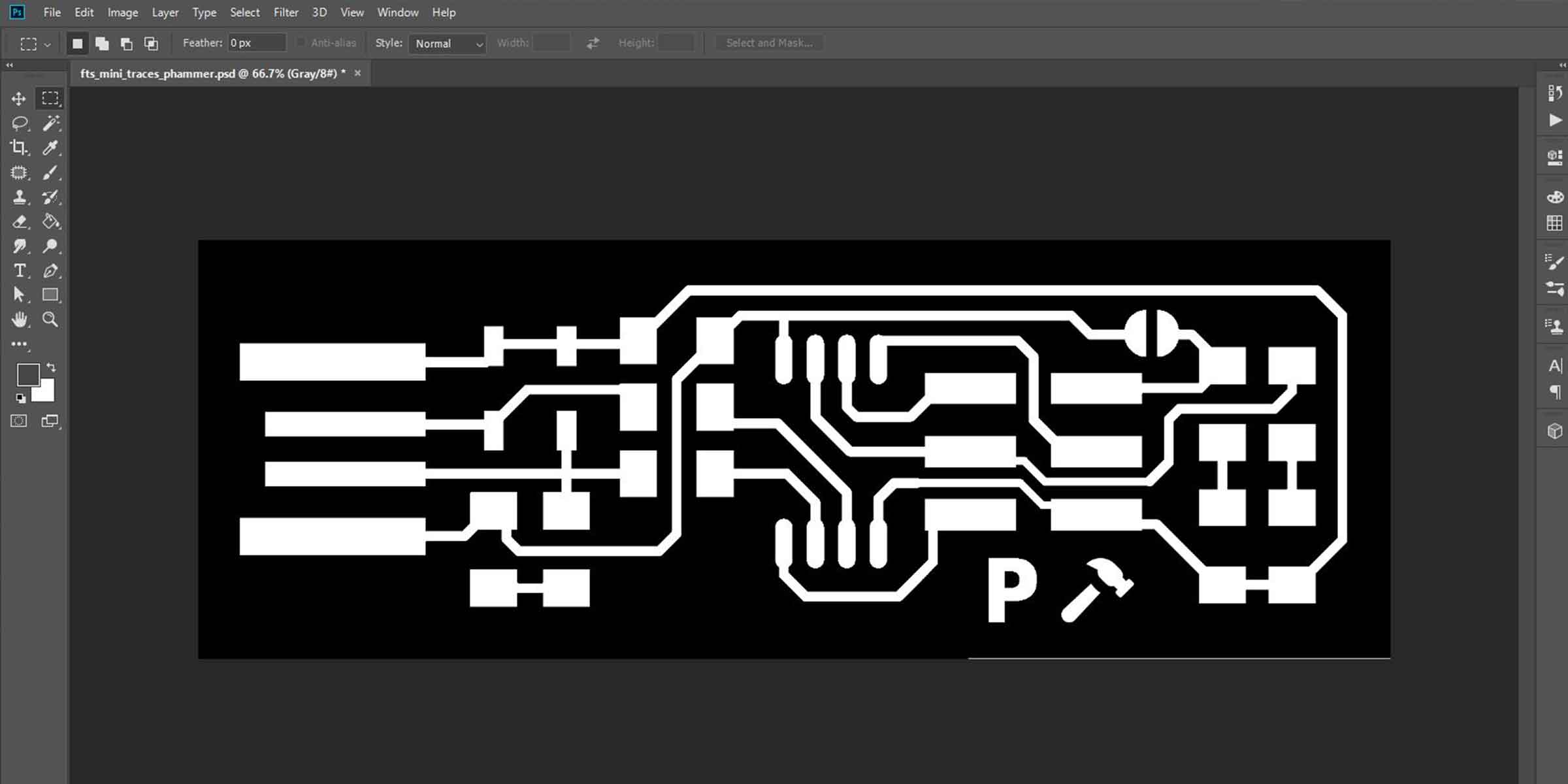
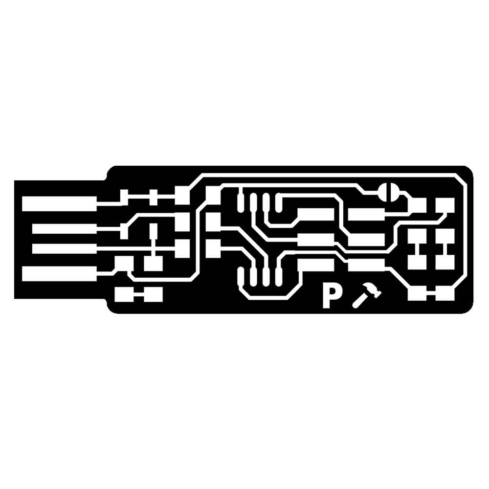
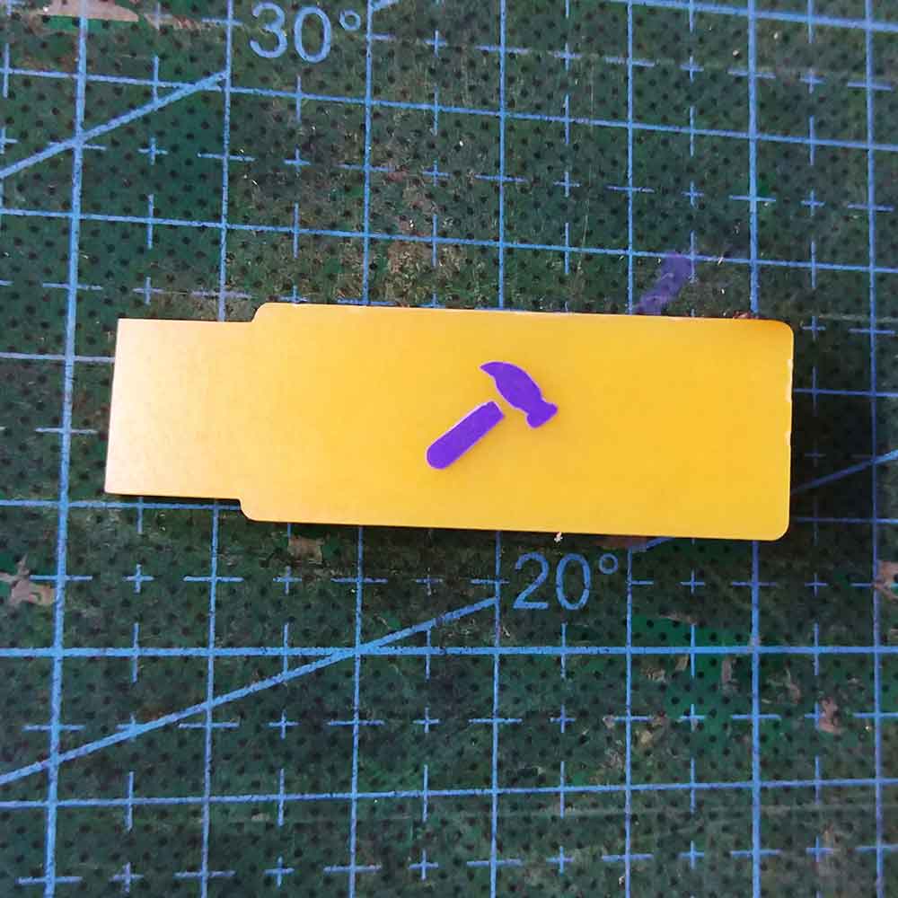
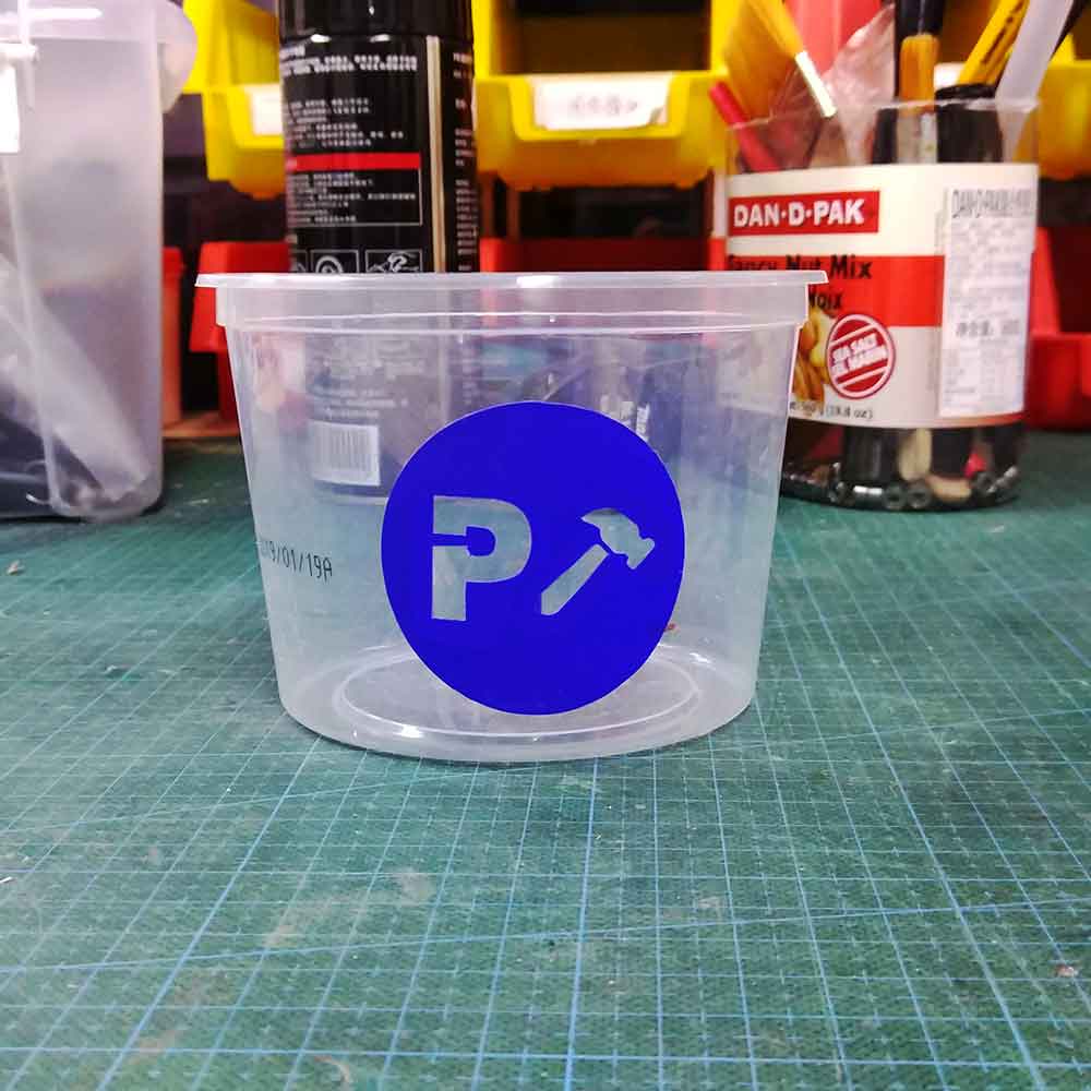
I decided to add my initial "P" plus a hammer icon (as my last names means hammer) in the FABISP file I
downloaded.
I did so by opening the file in Adobe Photoshop and adding the elements. It is super important that the
file remains the SAME SIZE (1000dpi), or else you will have issues with the board.
NOTE: when opening the files in Photoshop, as they are in BITMAP mode you have to change it to any other mode (I used grayscale), so you can add layers and work on your file. Afterwards save it as .PNG.
IMPORTANCE OF 0.4mm tolerance
It is very important to keep in mind that when doing the traces task, our circuit design should have a
gap of at least 0.4mm between each path/element on the board.
If the space between the paths/elements is below 0.4mm paths will intersect.
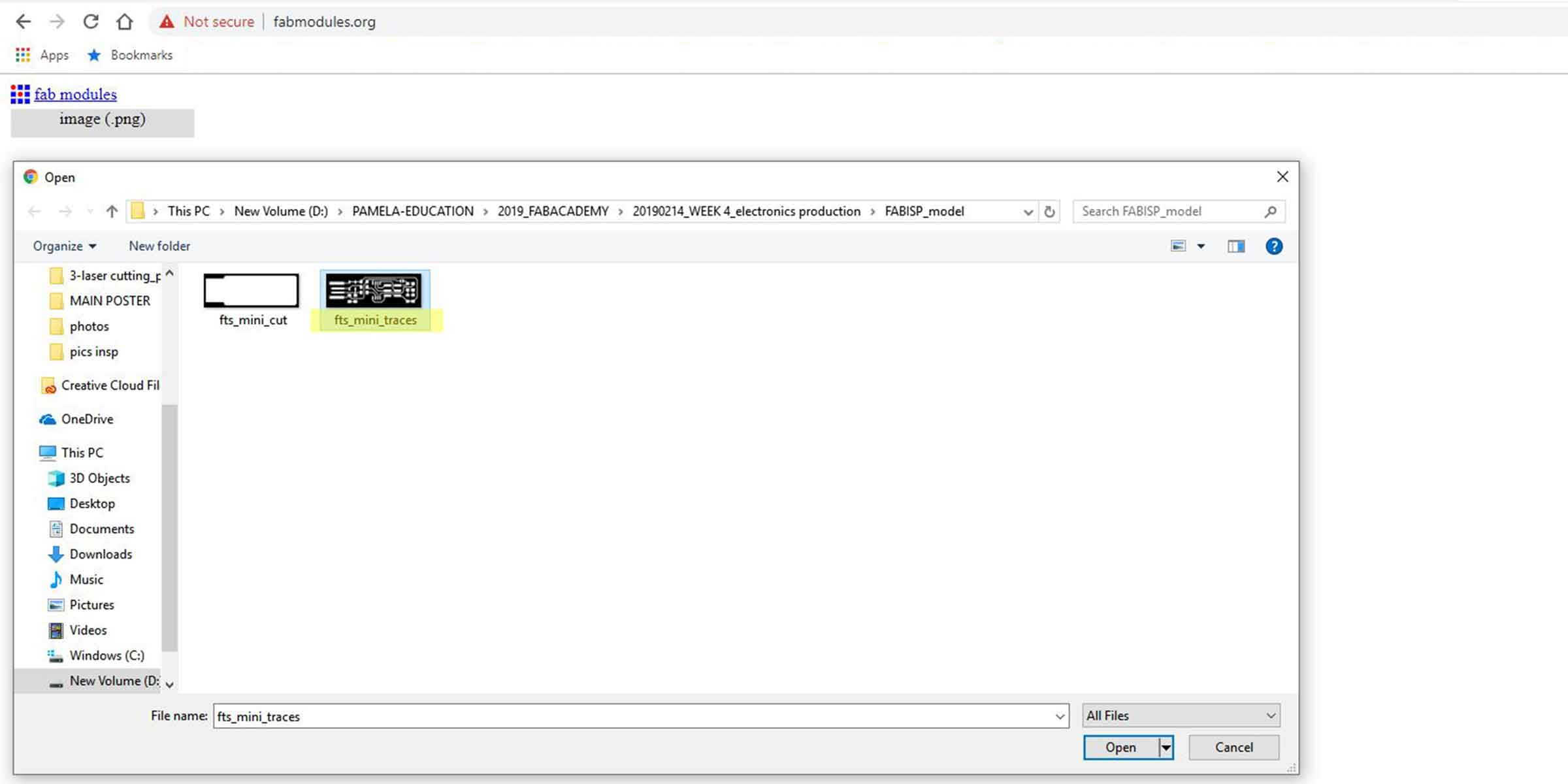
1_Set-up file for milling machine .rml
Using FabModules I set up the machine parameters for both the trace and outline files.
First select the file:
Then choose the output format (the machine you are using):
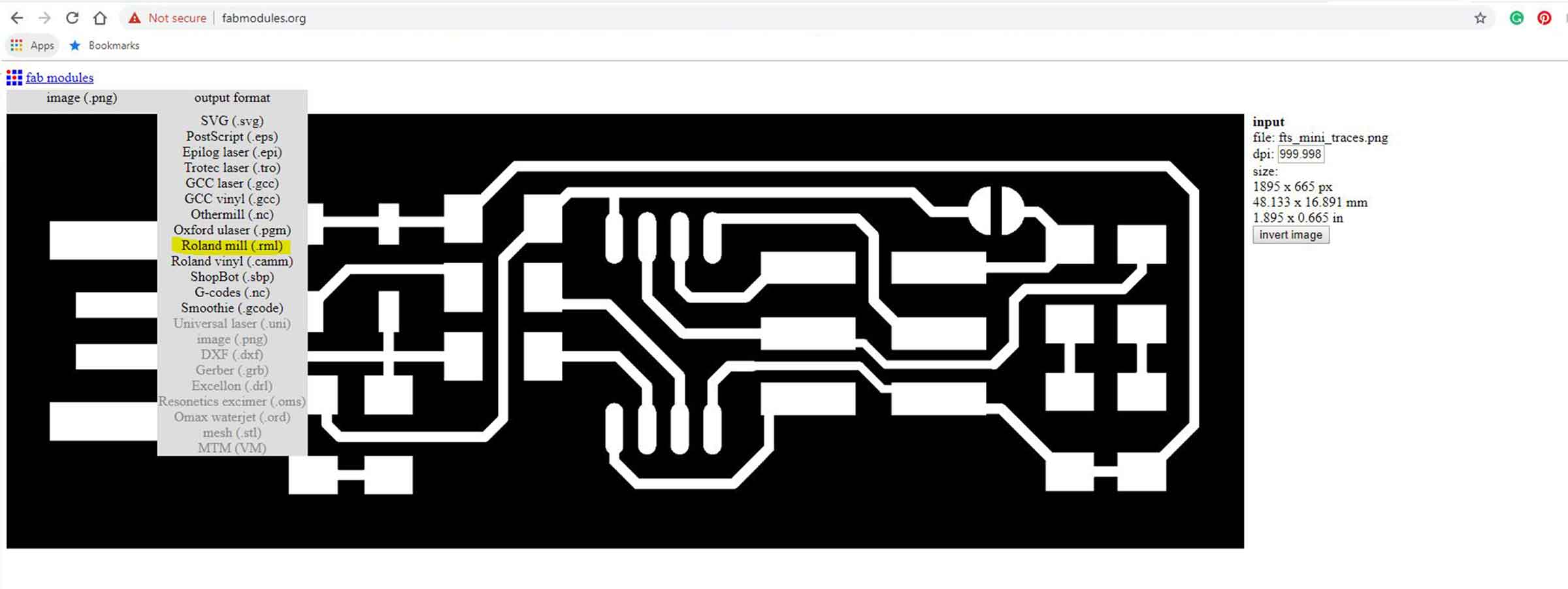
Here you have to choose what task you are doing, if it is the traces or the outline.
The value 1/64 is the tool size, which is expressed in inches, 1/64=0.4mm. Automatically when you select
this option, the next values will adapt to traces task.
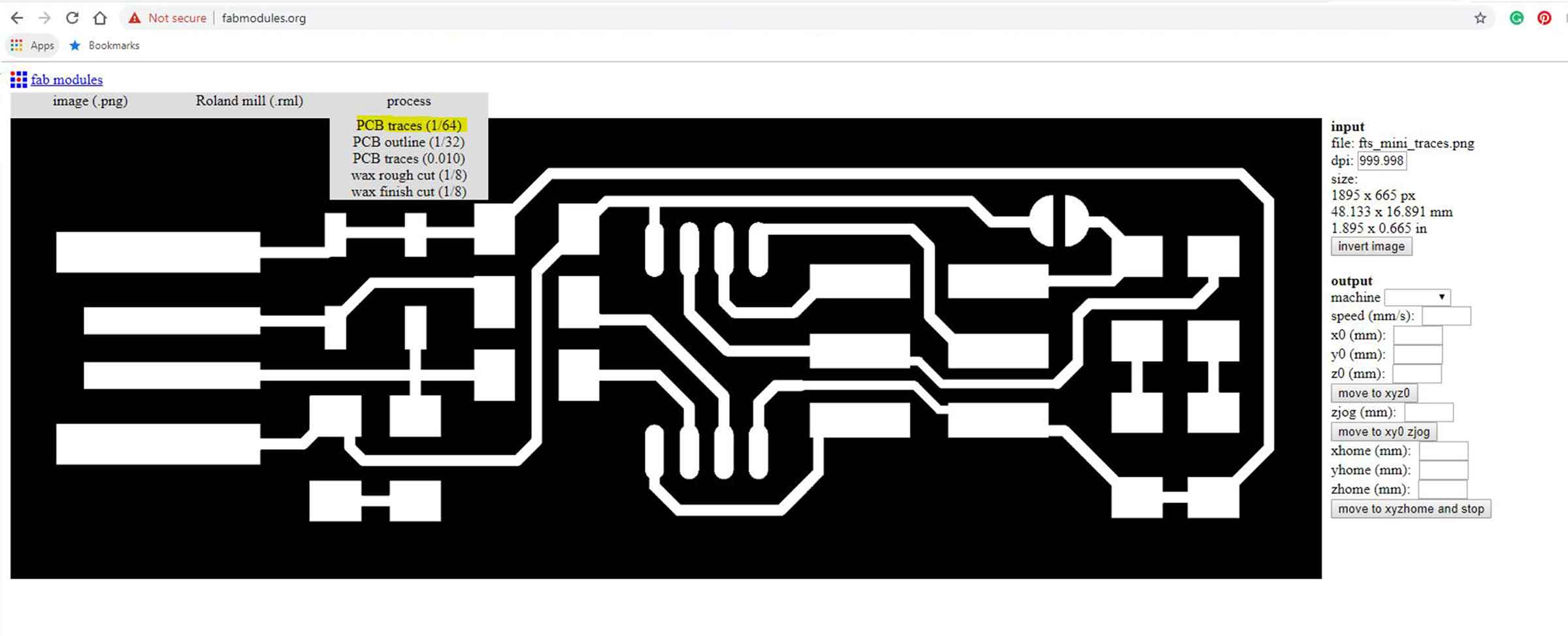
Note that XYZ are set to ZERO, this is because the user (us) defines the position.
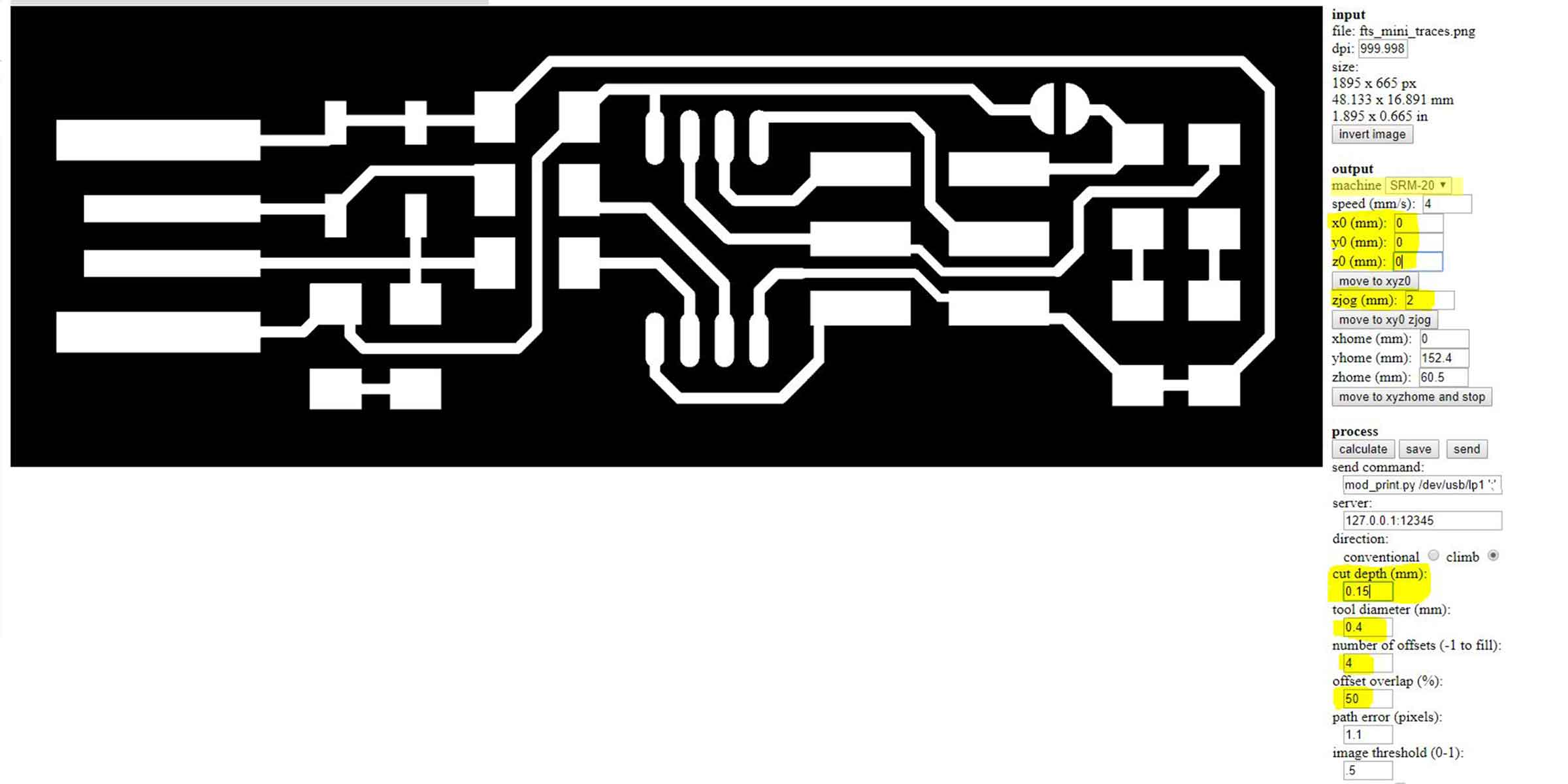
The most important values to keep in mind when doing traces, are highlighted in yellow, and they
mean:
_ZJOG is the height value that Z will jump every time it has
to jump from one point to the next one. Is good to keep a small value otherwise the task can take a long
time.
_Cut depth is how much material you want to remove from the
surface. Normally 0.1mm is enough, but if you want to make sure the material is being removed you can
use the value 0.15mm.
_Tool diameter is the drill beat we are using
_Number of offsets, is how many repetitions of the same path
has to do the machine. This is important because less than 4 offsets ay result on having a lot of traces
of copper on your board.
_Offset overlap, we use a value of 50, as we want the offset
to overlap exactly in the middle of the next path as this will make sure there are no traces of copper
left between the offsets.
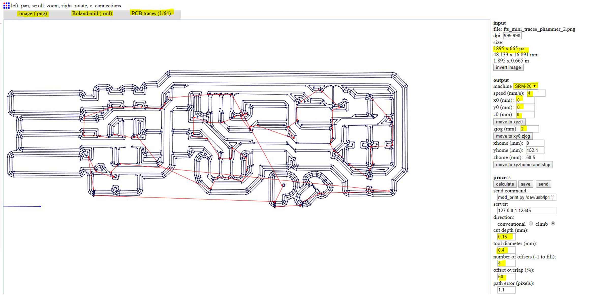
Then if you press the buttom calculate, the program will show you the travel paths and this is very
useful because it allows you to check if there are no errors such as paths being to close to each
other.
The blue is the path the drill will follow, the red are the ZJOG jumps.
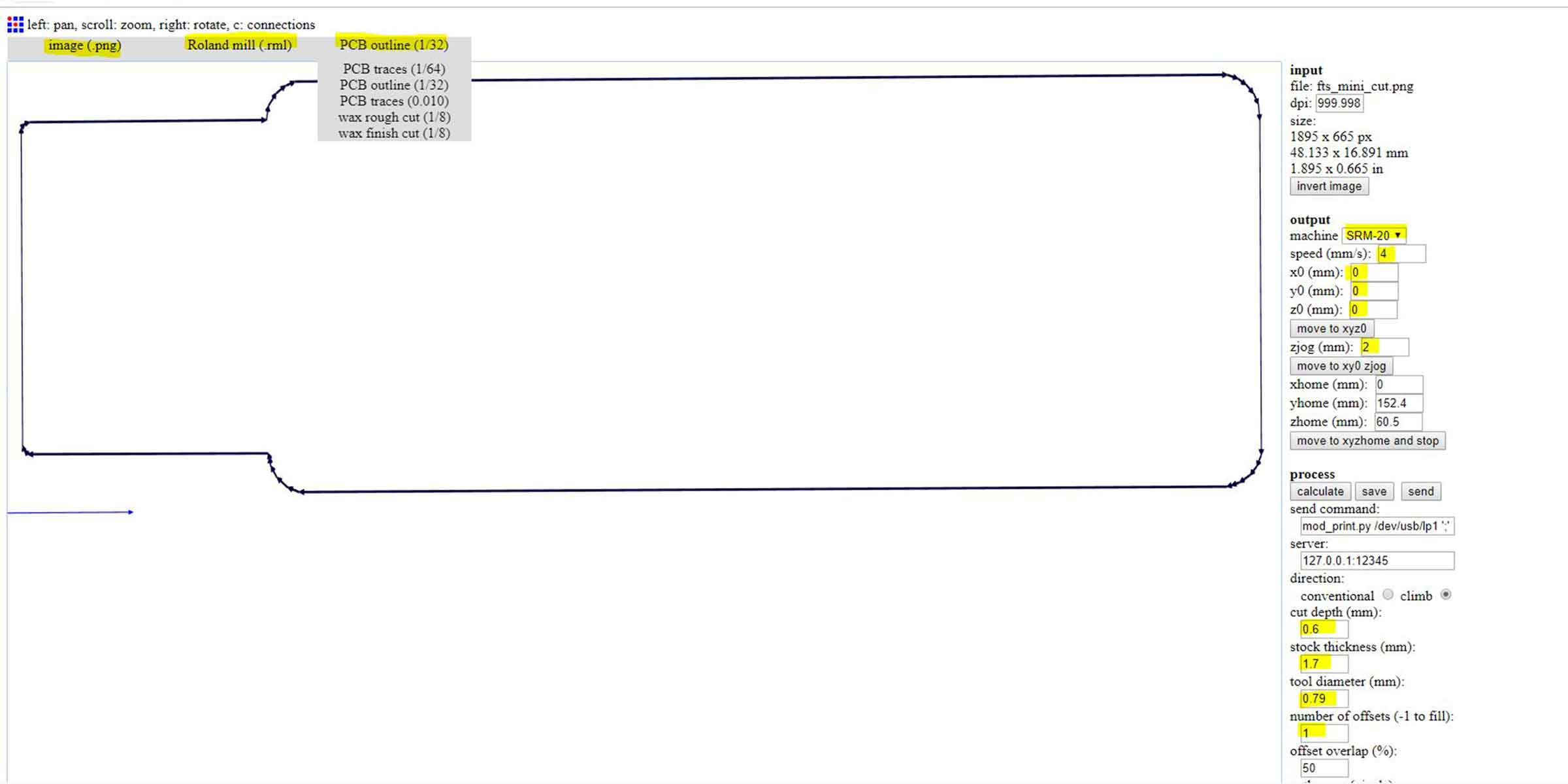
I did the same process for the OUTLINES, but in this case the outline is set to 1/32 (0.8mm).
Other values that you need to keep in mind when doing the OUTLINES, are:
_Cut depth, this is how much material you want to remove each time.
As the sheet has a thickness of
1.7mm, it is not recommended to set the cut depth to the same size, this is because you could easily
break the drill beat, so it is better to do several times the cut.
We set the value to 0.6mm and the program will calculate how many times it has to repeat the task in
order to arrive to the material thickness (in this case it will do it 3 times).
This value 0.6mm is good, if you use for instance 0.7mm the machine would do 0.7mmx3 times=2.1mm and
this would result on removing more material from the sacrificial layer. So is better to set a lower
value that repeats more time and removes less material as well from the sacrificial layer.
_Stock thickness, this is the thickness of the material.
_Tool diameter, the size of the drill beat.
_Number of offsets, there is only one path as we are doing an outline.
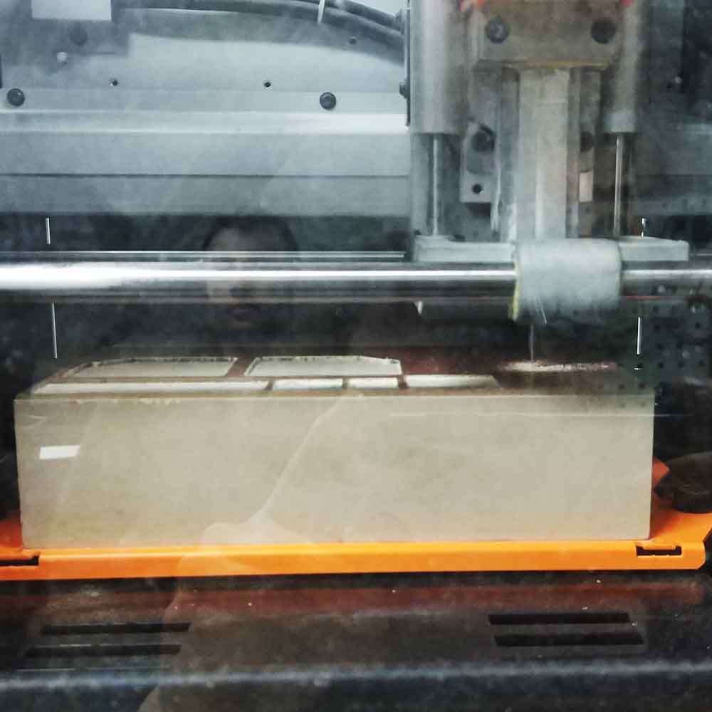
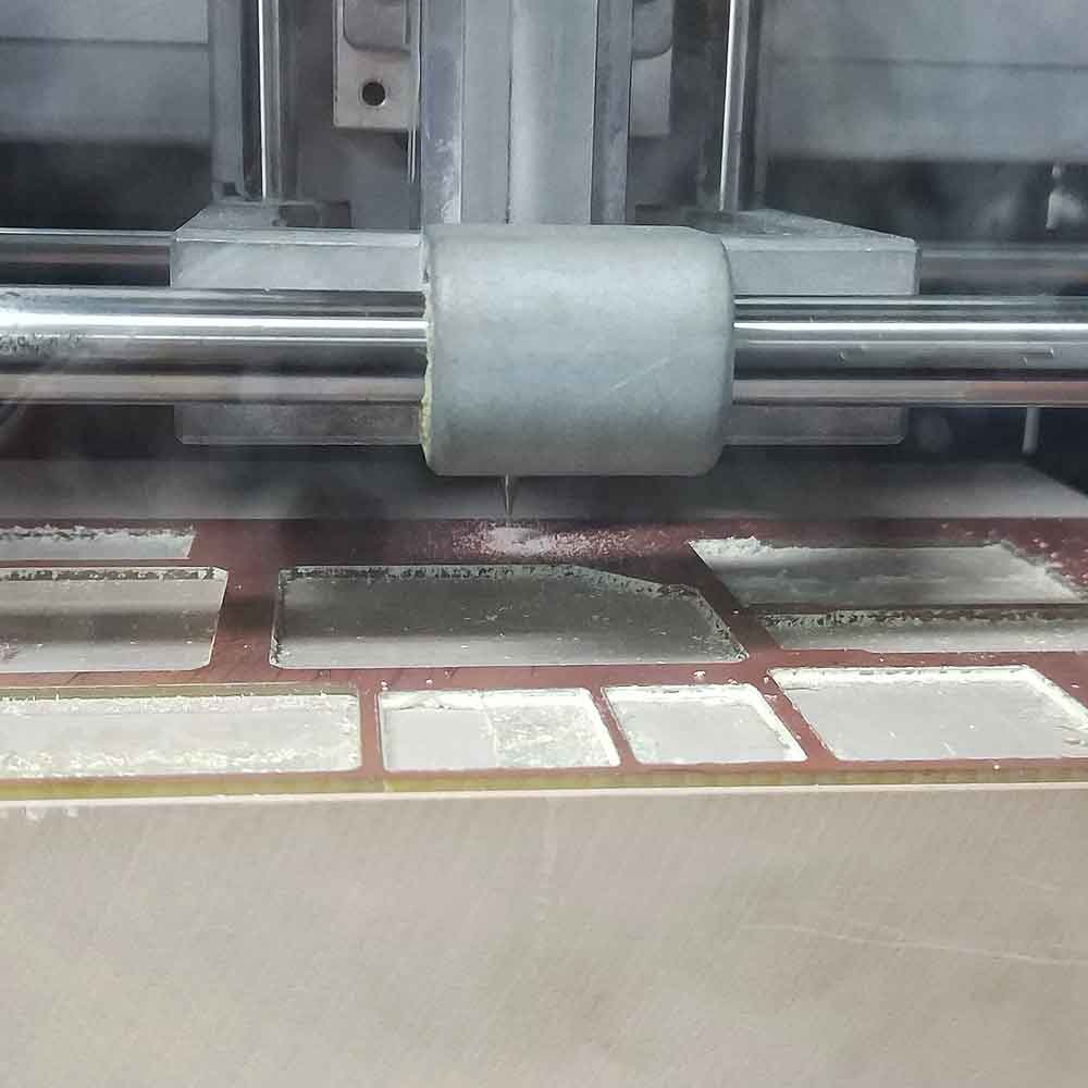
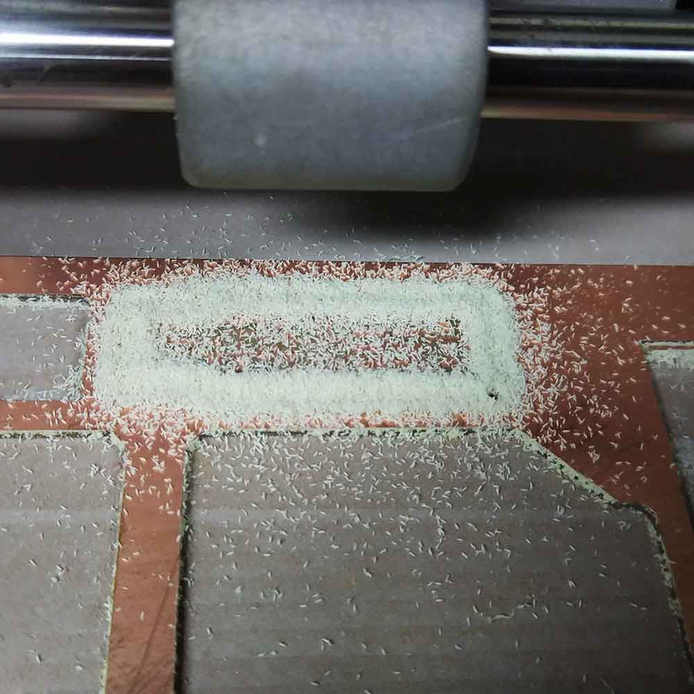
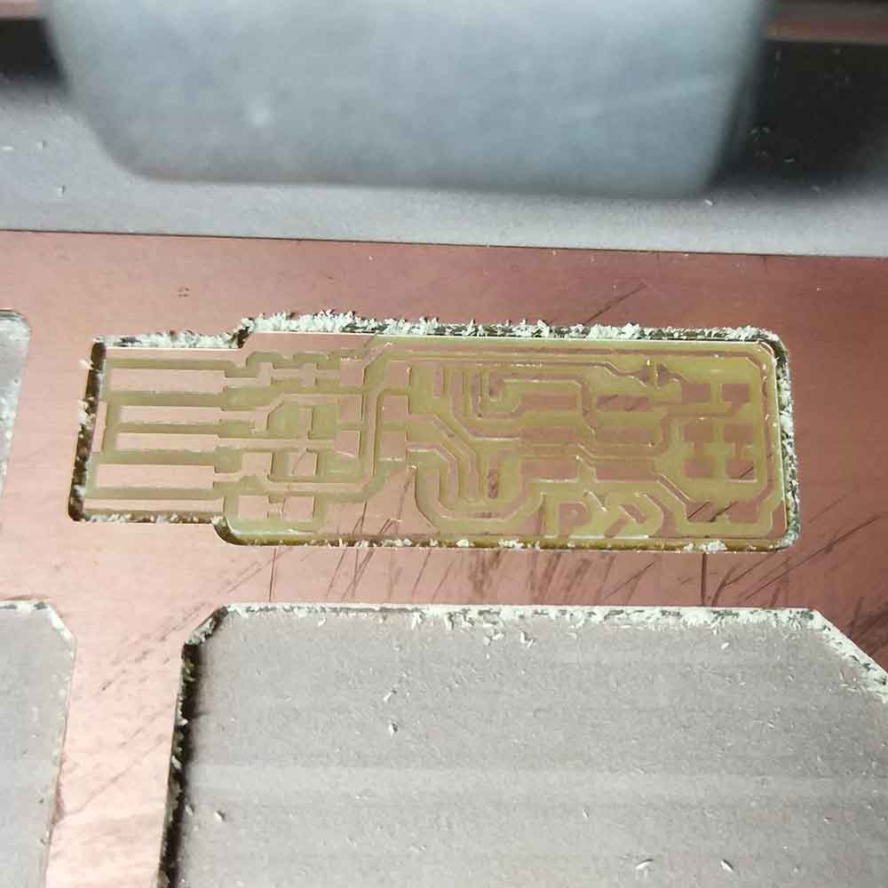
2_Milling cut process
Once I had my file ready, I set up the milling machine axis and started the tasks.
As mentioned above, the type of material we are using is a laminate material, and the one we used is
called FR1 which is a phenolic paper and is easy to mill, as instead of the FR4 which is a
glass-reinforced epoxy laminate material, that is stronger but not recommended for milling.
This is an example of the FR1 we are using(photo taken from internet).
Here are some photos of the milling cutting process and results:
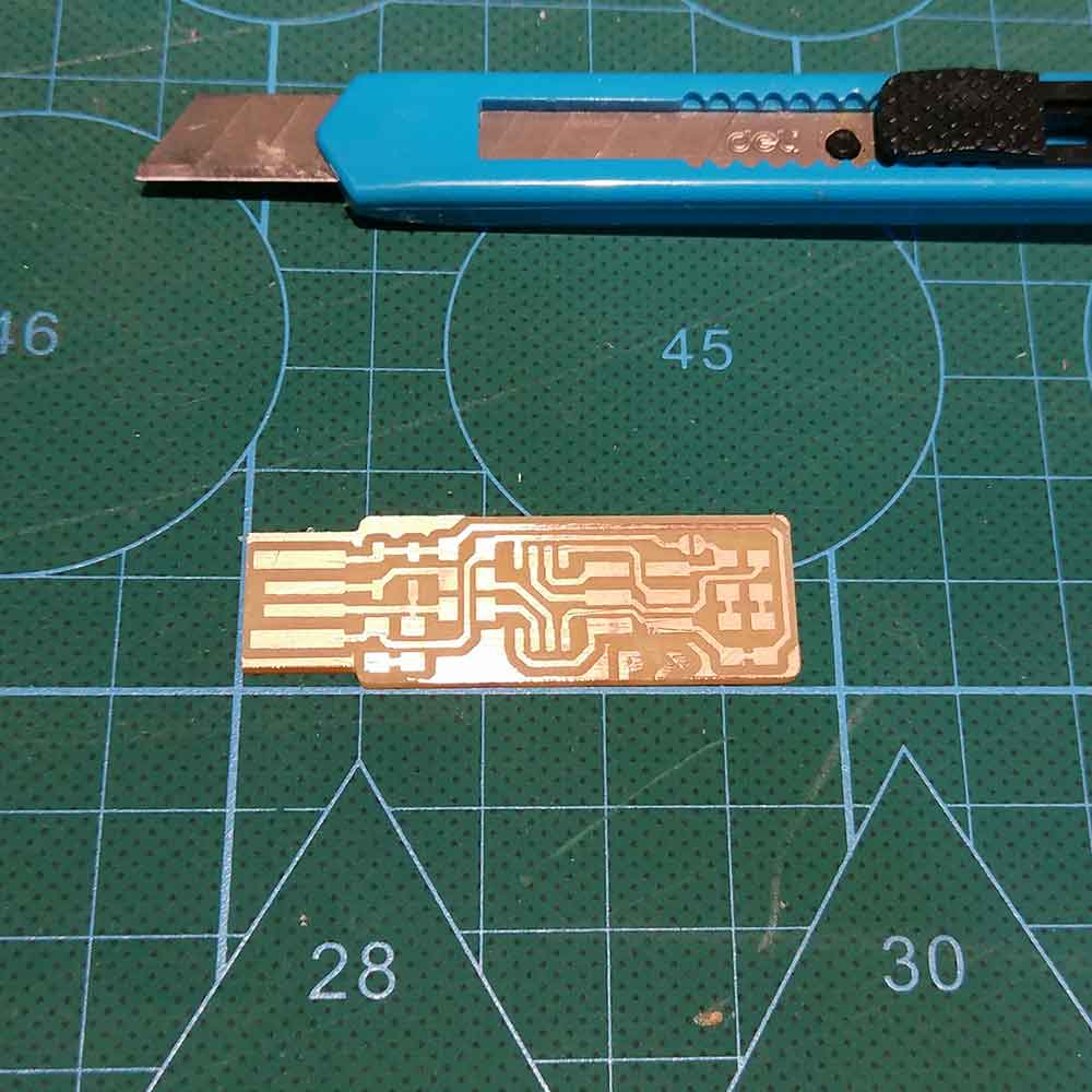
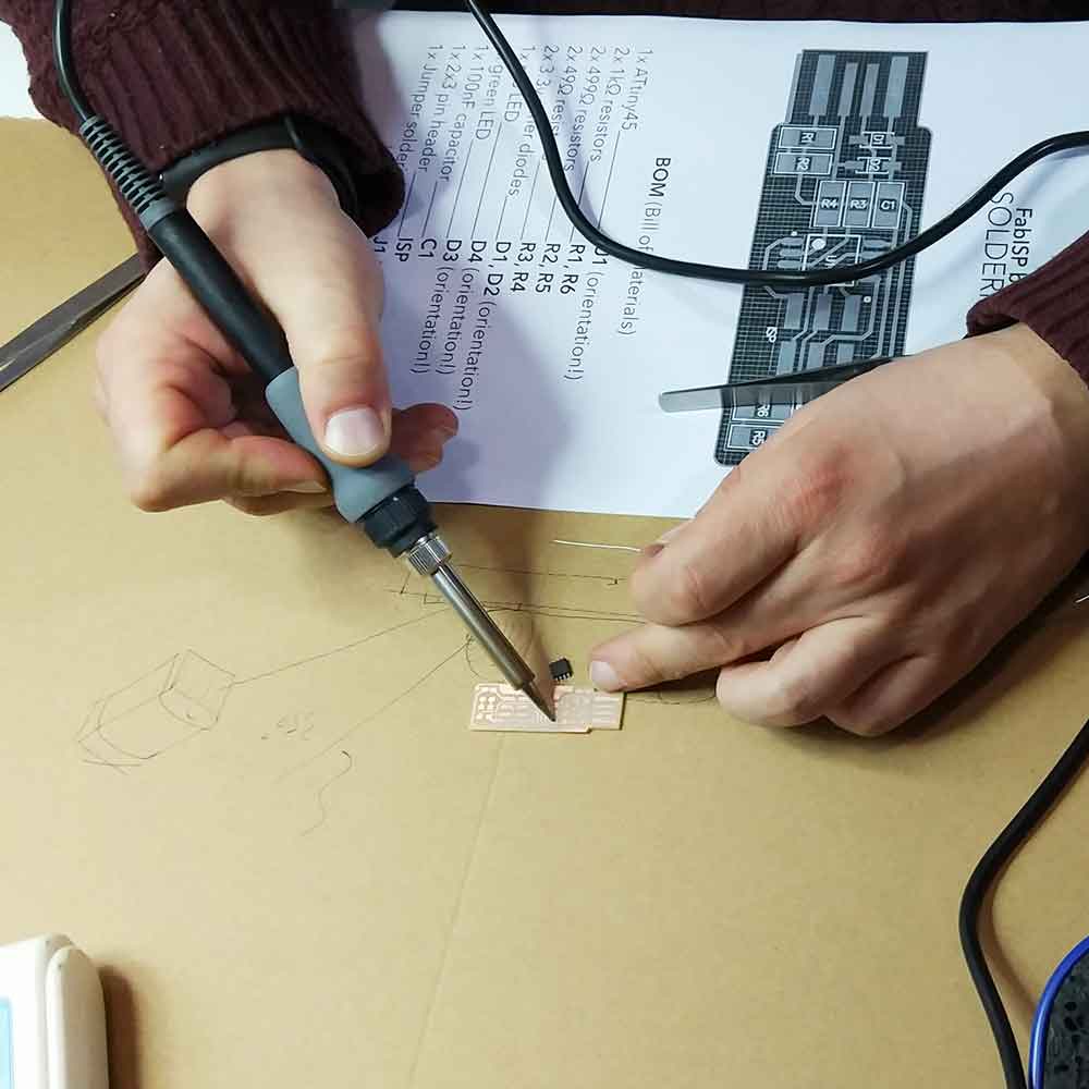
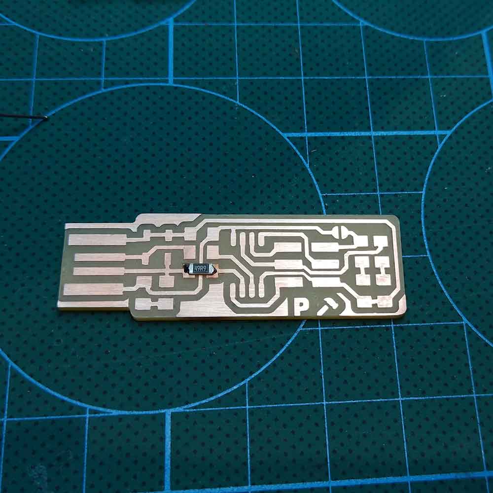
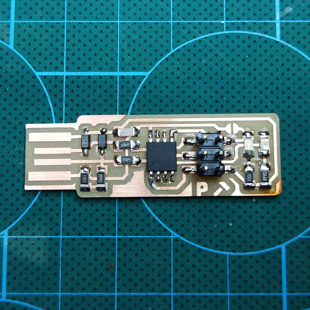
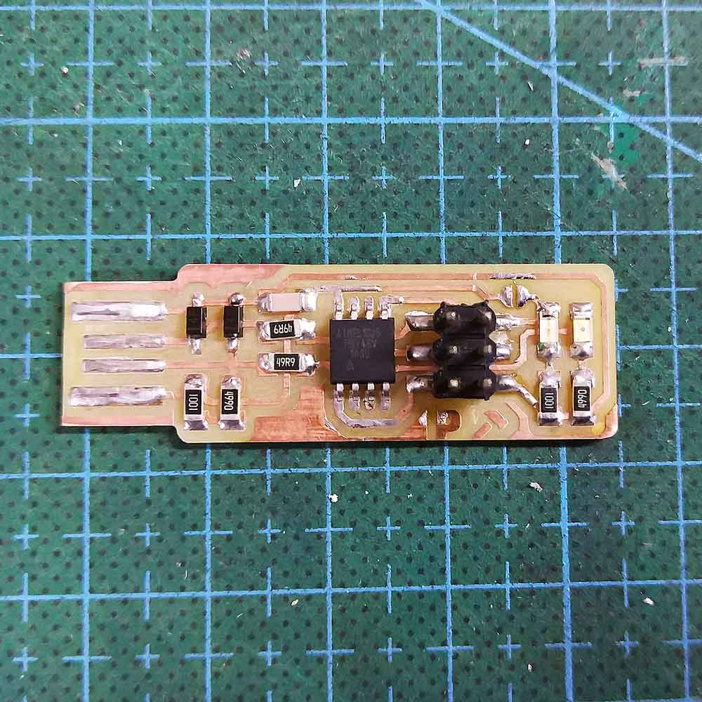
3_Assembling the PCB
Once I finished cutting the board, I used a very thin sand paper to clean it and leave the surface
smooth.I then cleaned the surface using acetone.
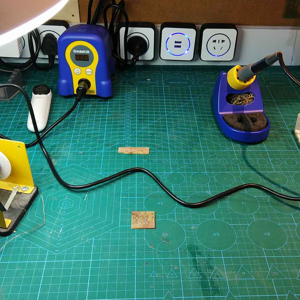
After this process, it comes the fun part, the assembly. For that we need the components that will make
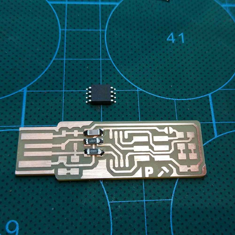
our FABISP work. Here is the list of the components used, which are available in our Lab:
_1x ATtiny45
_2x 1kΩ resistors
_2x 499Ω resistors
_2x 49Ω resistors
_2x 3.3v zener diodes
_1x red LED
_1x green LED
_1x 100nF capacitor
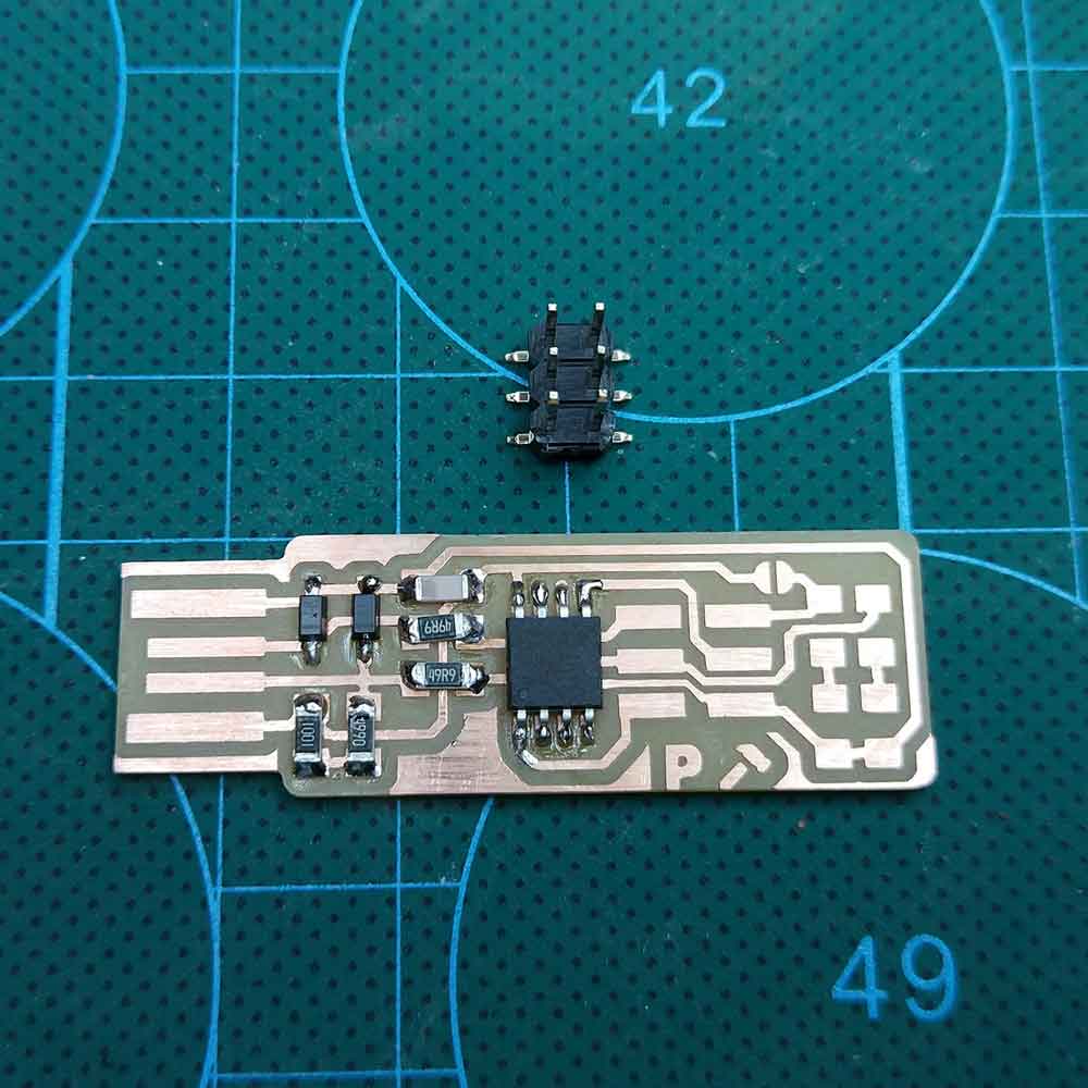
_1x 2x3 pin header
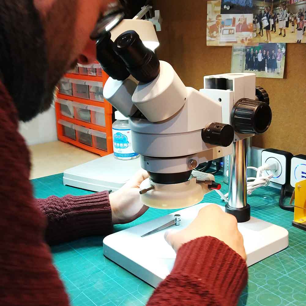
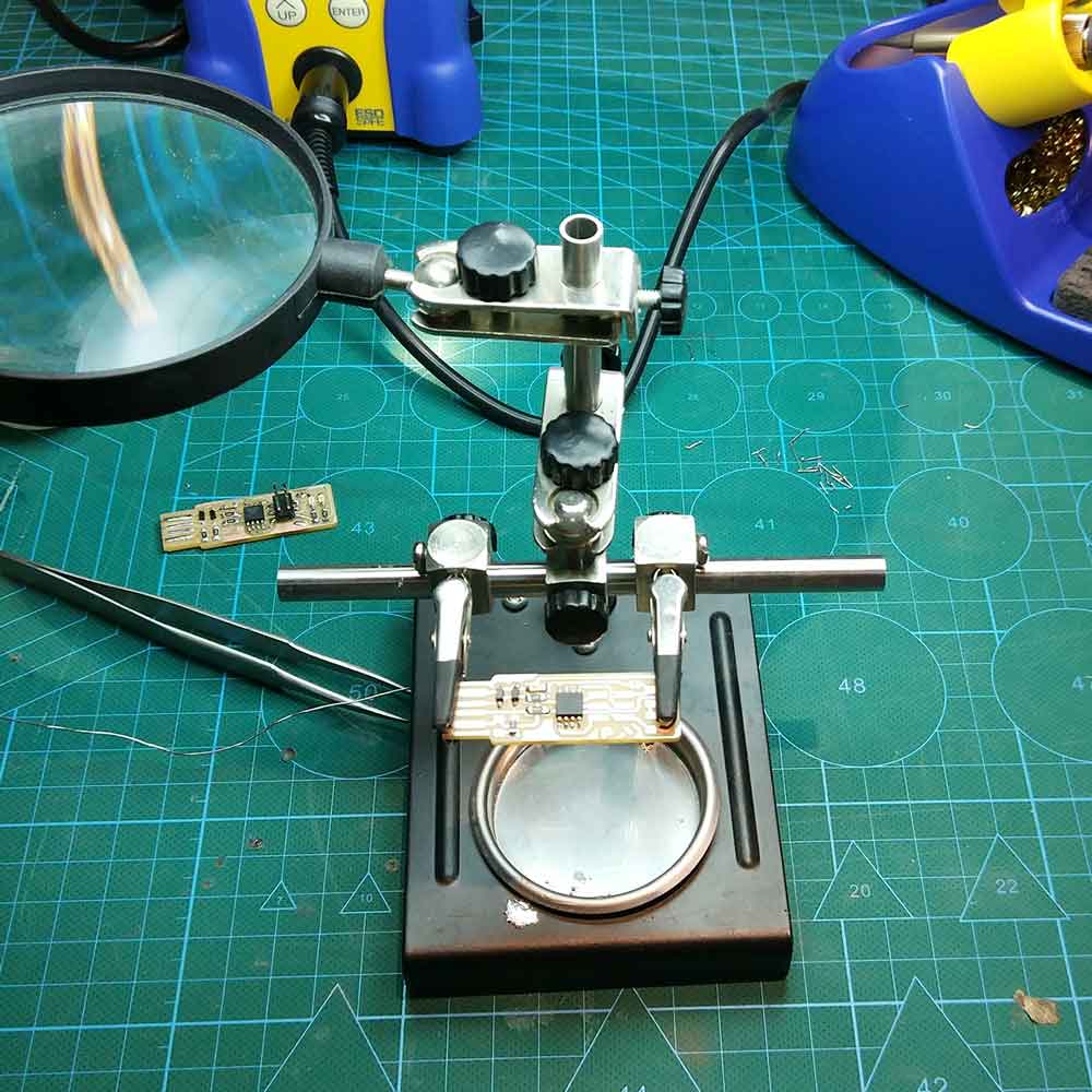
Is good to note that the type of soldering we will be doing is called surface mount soldering SMD, as there are other types of soldering such as through-hole THT.
Besides the components you will be needing this tools as well:
_soldering iron (we set it to 350C degrees)
_soldering iron stand with sponge (has to be wet)
_soldering wire (tin, lead-free)
_desoldering wick (super useful to remove excess of soldering)
_tweezers
_magnifying glass/lamp (recommended)
_wrabbing arms (not needed but sometimes they help)
_and something essential, good lighting!
It's useful if you print the schematic to guide you on which components go where. You can find it on Brian's website as well.
TIP: Before I started soldering I read and watch some extra tutorials about how to solder, as there are several techniques which are all valid but you need to discover which one suits you best.
Here are some useful links about soldering:
_how to solder
_surface mount soldering
_soldering a pin header THT
_soldering and desoldering surface mount
components
After reading and watching some tutorials I did some tests on an old PCB we had at the lab.
I solder a couple of capacitors and did a few tests desoldering as well.
Once I felt a bit more confindent I decided to start on my FABISP.
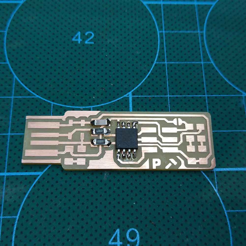
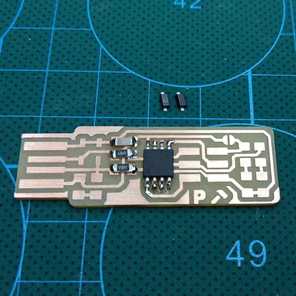
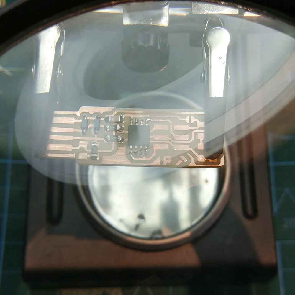
When soldering the LEDs it was tricky to find the correct position to solder them, but using the multimeter you can find the "ground" and locate the LEDs in the correct position.
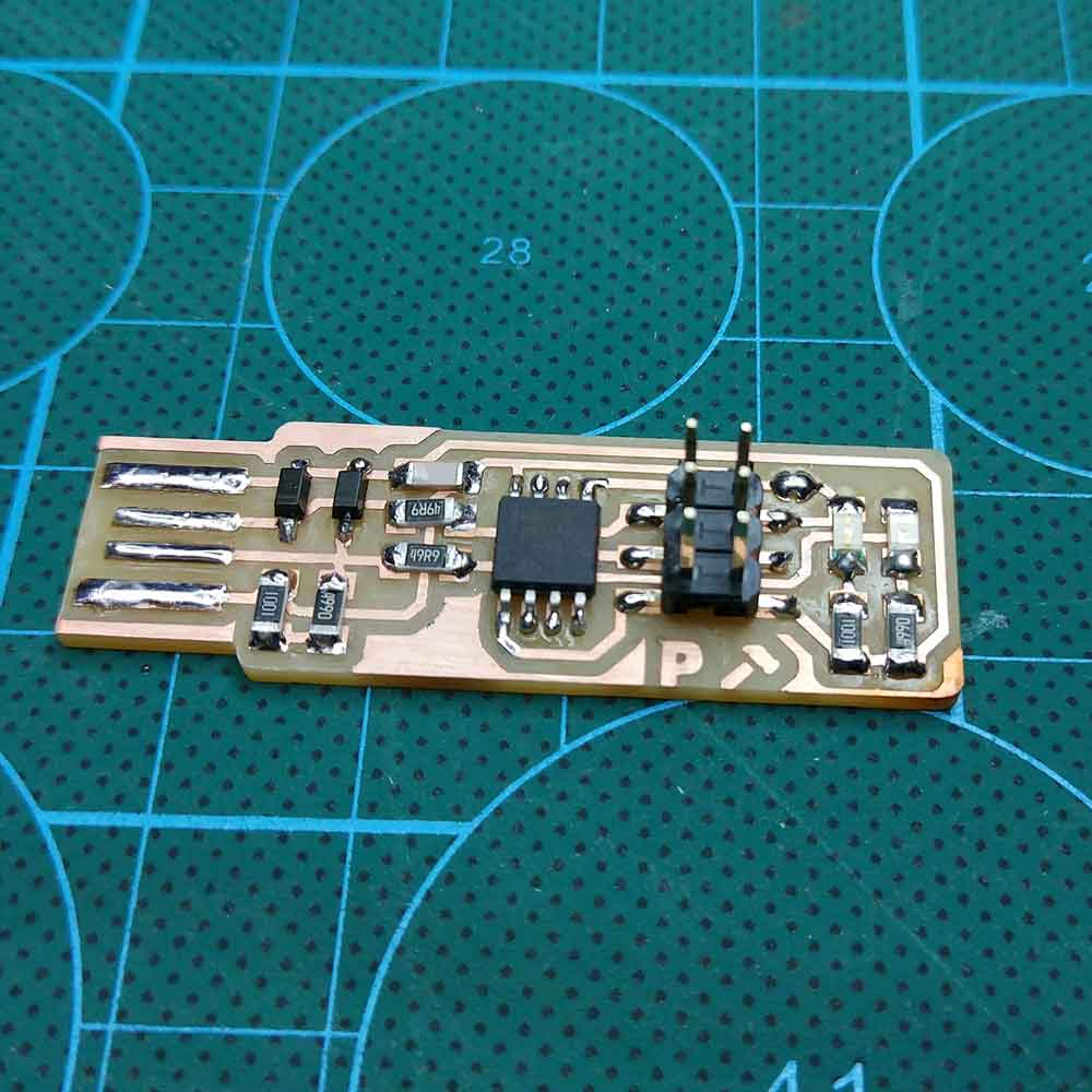
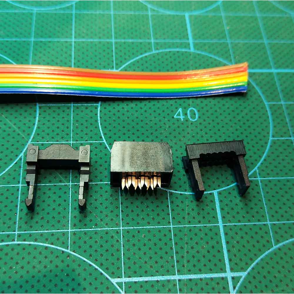
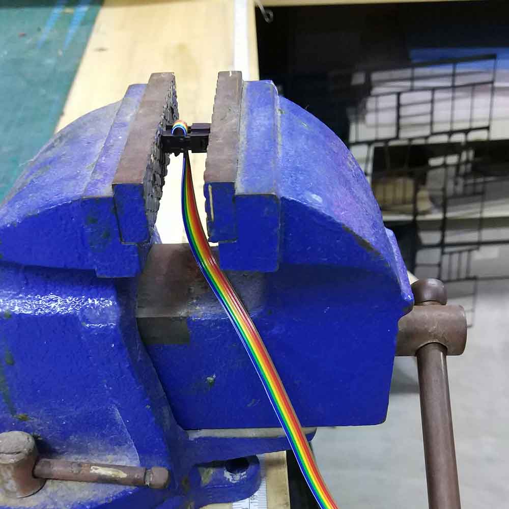
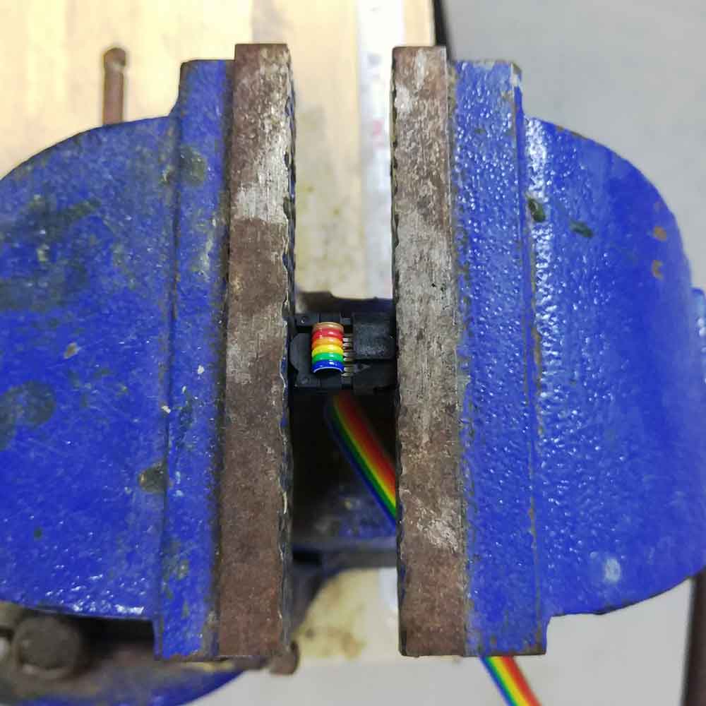
IDC ISP cable:
You will need an ISP cable to connect your newly made FABISP to the programmer.
For that you just need a 6 way flat cable and 2 pairs of 6 pin (2x3) crimp-on IDC connectors.
You have to be careful when assembling your cable, both pins have to face the same direction.
Below is the process on how to assemble them.

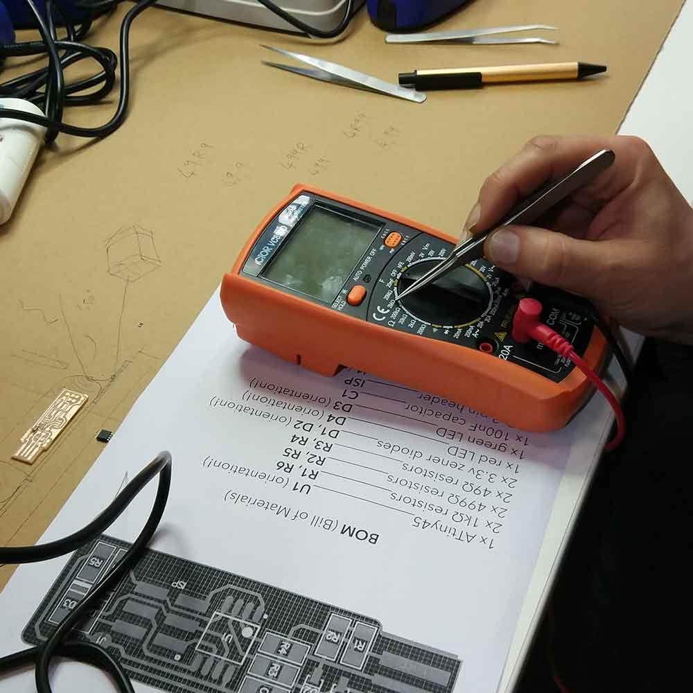
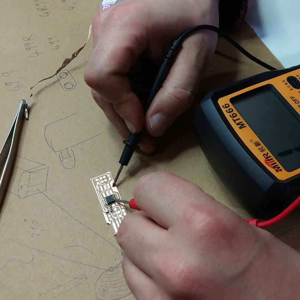
IMPORTANT ADVICES
After finishing soldering your board, you should do the following:
1_Clean it very well with alcohol
2_Check the continuity of the componenets using the multimeter
3_Check there are no short circuits
4_Check that the soldering went through the components "legs". It has to flow btween the pin and the
copper pad.
5_Check if you put enough soldering, sometimes when it's too little there might be connection
errors.
6_Check that the componenets are not connected them.
4_SOFTWARE INSTALLATION ON WINDOWS 10
For the software installation I followed this detailed guide from Brian's website: click here.
Here is what I did step by step:
1_Download and install AVR 8-bit Toolchain v3.62 –
Windows.
Save it on your local DISC C, inside Program Files.
2_Download and install GNU MAKE. Save it on the
default location.
3_Download and unzip the avrdude folder inside your
local Disc C-Program Files.
4_Now you have to update your PATH, basically it's telling Windows where are all the tools you've
installed.
To do so go to: Control Panel>System & Security> System and select "Advanced system settings".
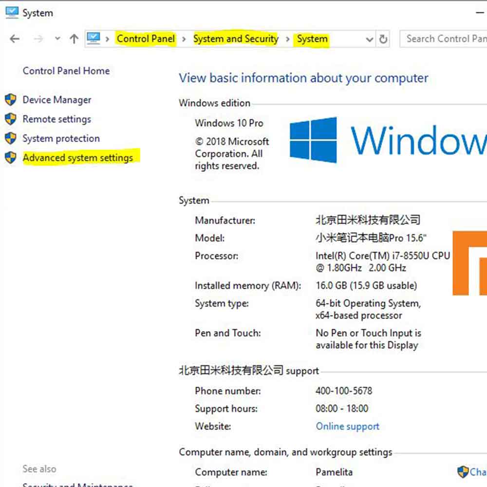
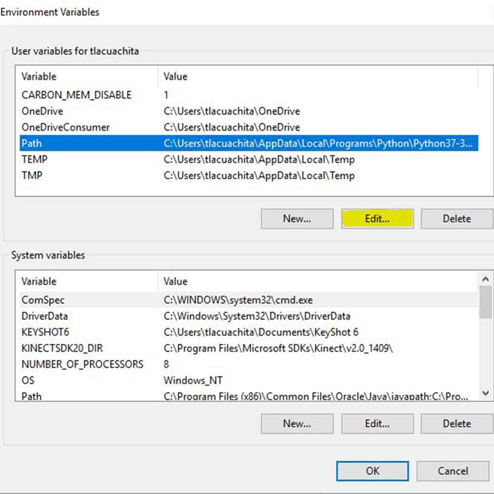
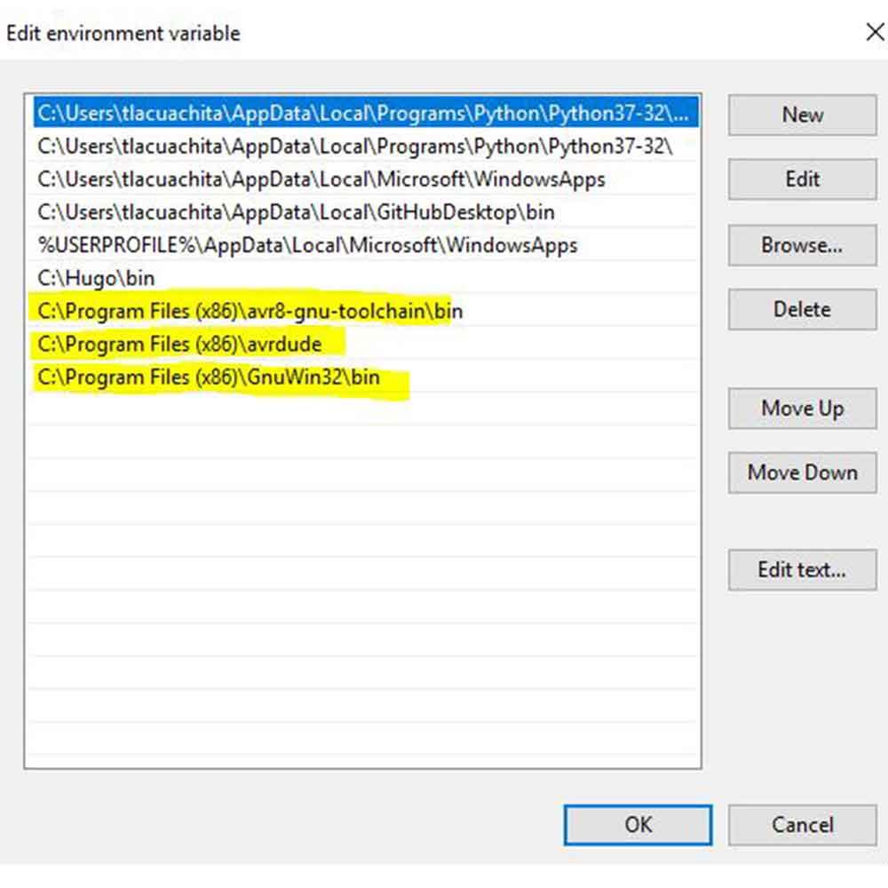
You have to update the PATHS, if you can't see them you will have to add them but they should be the same
path where you installed or copy the softwares.
Make sure you have these 3 paths:
-C:\Program Files(x86)\avr8-gnu-toolchain\bin
-C:\Program Files (x86)\GnuWin32\bin
-C:\Program Files (x86)\avrdude
5_Download and launch zadig.
For this software you will need to do this once, connect your programmer (the mother ISP where you are
copying the firmware from).
When the menu pups up choose: USBtinySPI on the top bar, then below besides the green arrow, choose
ibusb-win32 or libusb0. Then click INSTALL DRIVER.
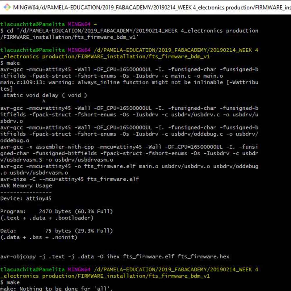
6_CHECK THE SOFTWARE INSTALLATION
Open your GITBASH and run the following commands:
make -v avr-gcc --version avrdude -c usbtiny -p t45
You should get the following results on your GITBASH:
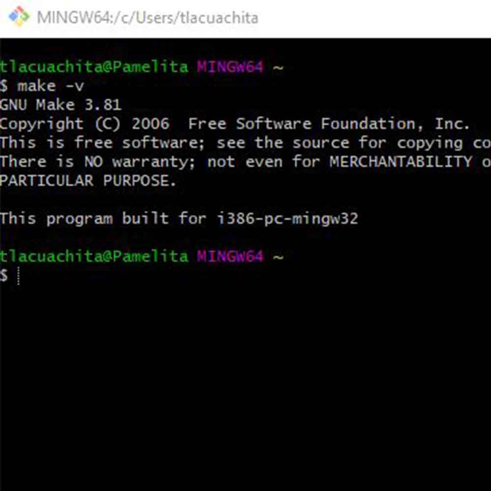
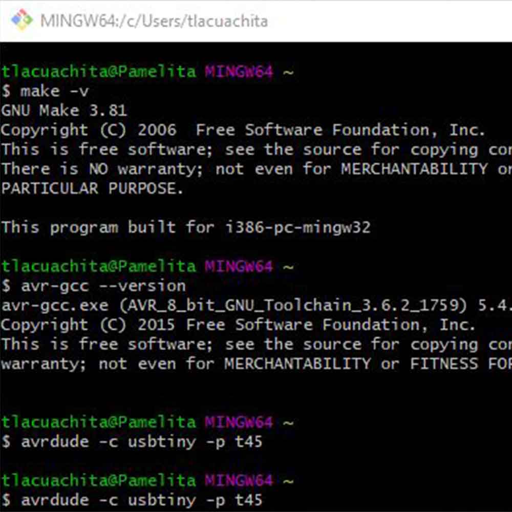
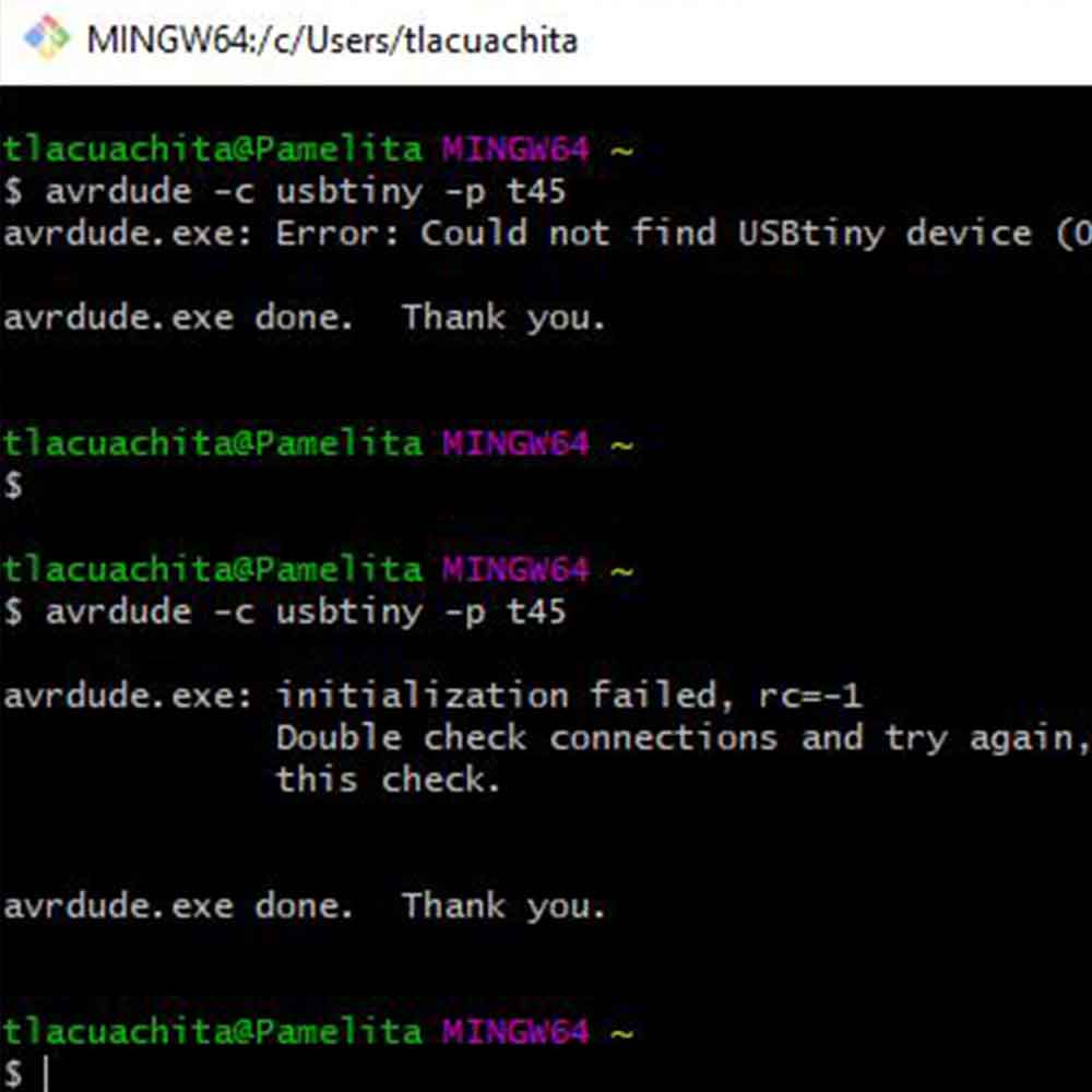
(If you get "initialization failed, rc=-1" means that avrdude run correctly as it found the programmer but not the new FABISP, this is normal as it was not connected at this point, so is ok.
7_COPY THE FIRMWARE FILE
Download the firmware that is available on Brian's website under "GET AND BUILD
FIRMWARE".
You have to unzip the folder, and save it, then run GITBASH change directory and find the root directory
where you saved the firmware.
Then run:
make
You should get this message if everything went well:
Inside the firmware you just copied there is Makefile, this file by default has a usbtiny (like a
FabISP) as a programmer.
As we used another FabIsp to program our new FabIsp, we don't need to change anything on the Makefile,
but you should change it if you are using another type of programmer, and you probably have to change
the speed as well.
8_CONNECT AND PROGRAM YOUR FABISP
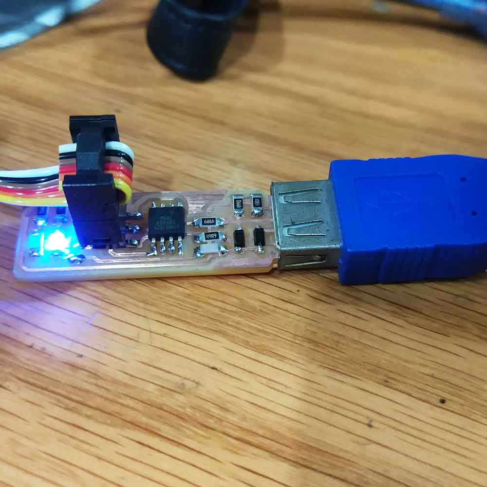
At this point, you have a general idea of how this will work, we need to copy the firmware into our new board, so the connections should be looking like this:
I connected my FABISP to an external source of power and the LEDs lights on my board turned on, that's a good sign!! but it doesn't mean it's done.
Now check that the ISP cable is connected with the same orientation on both boards.
After this connect connect the programmer to your computer, open GITBASH and run:
make flash
ERROR! MAKE FLASH DOESN'T WORK
Ideally, checking all the above my FABISP should be working but I got this error:
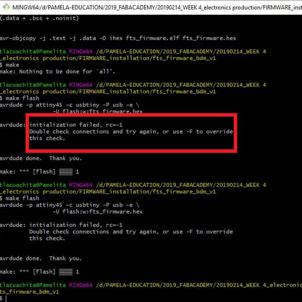
Fortunately helped by my instructor Saverio, we managed to fix the problem, we are not entirely sure what
was the issue but we did the following to solve it:
1_Desolder ATtiny45 and solder a new one.
2_Improvement of the soldering joints of the pin header (we added more soldering).
3_Clean! We used alcohol to clean the board (not acetone at this point that we have all the components
joined)
After this we reconnected the board and ran once again:
make flash
Now we got this message:
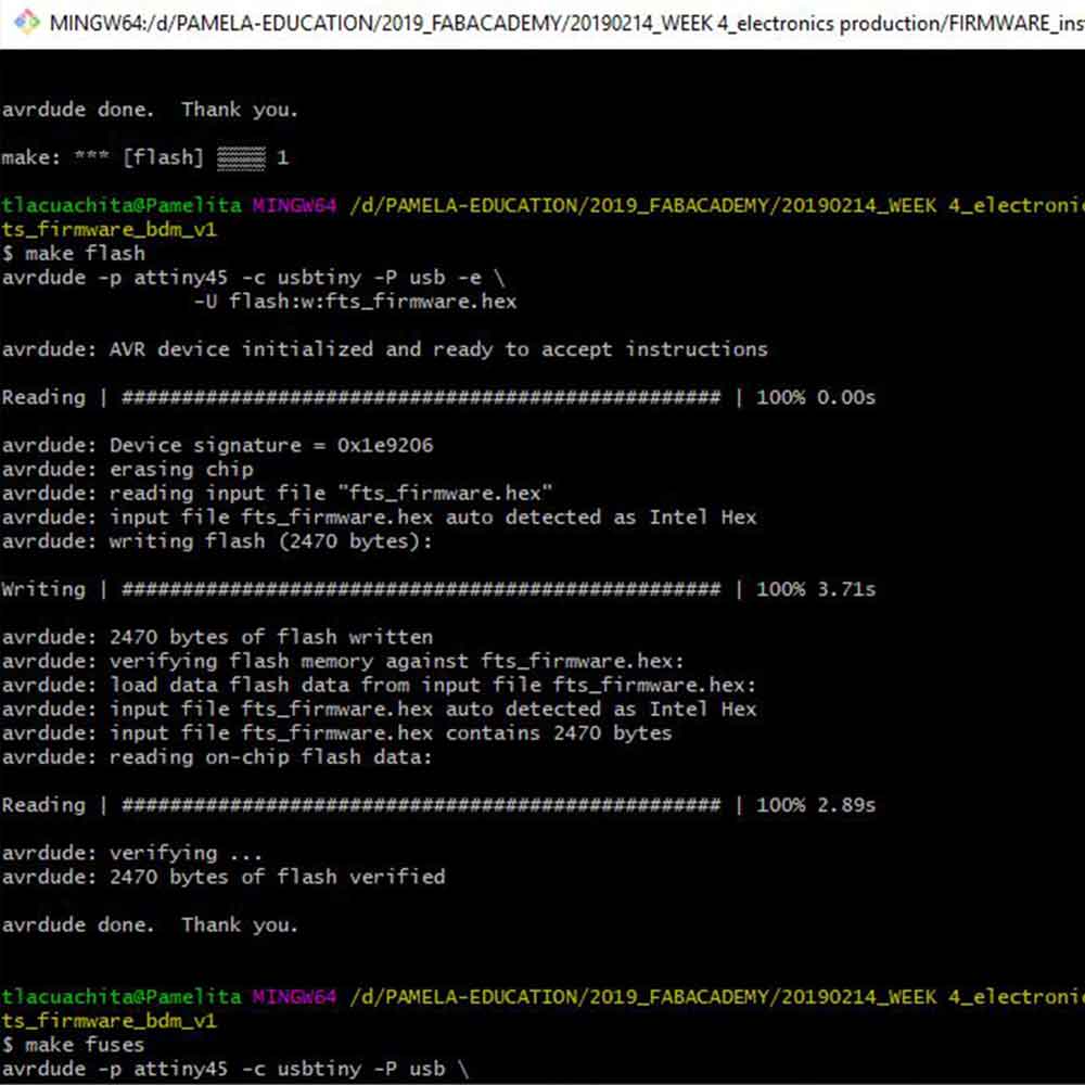
Then you have to run:
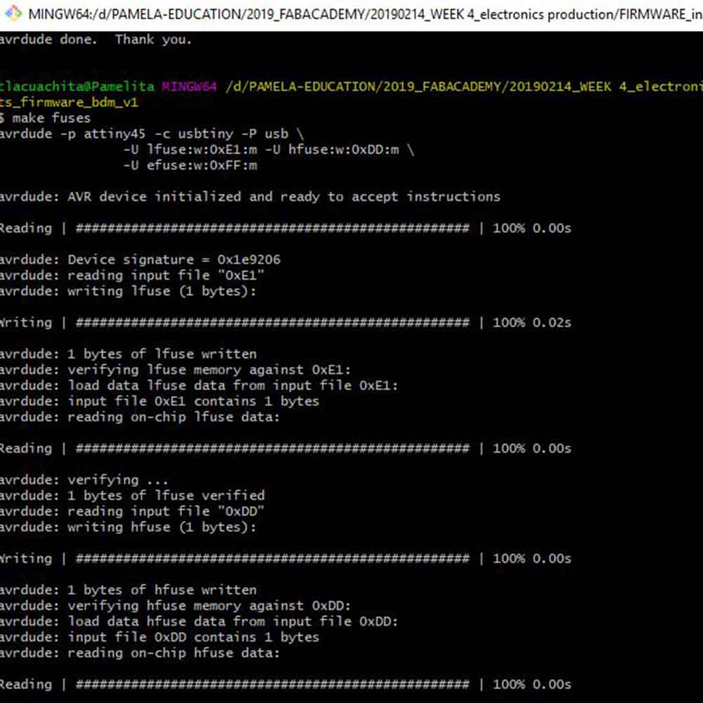
make fuses
Which fortunately worked and this message was shown:
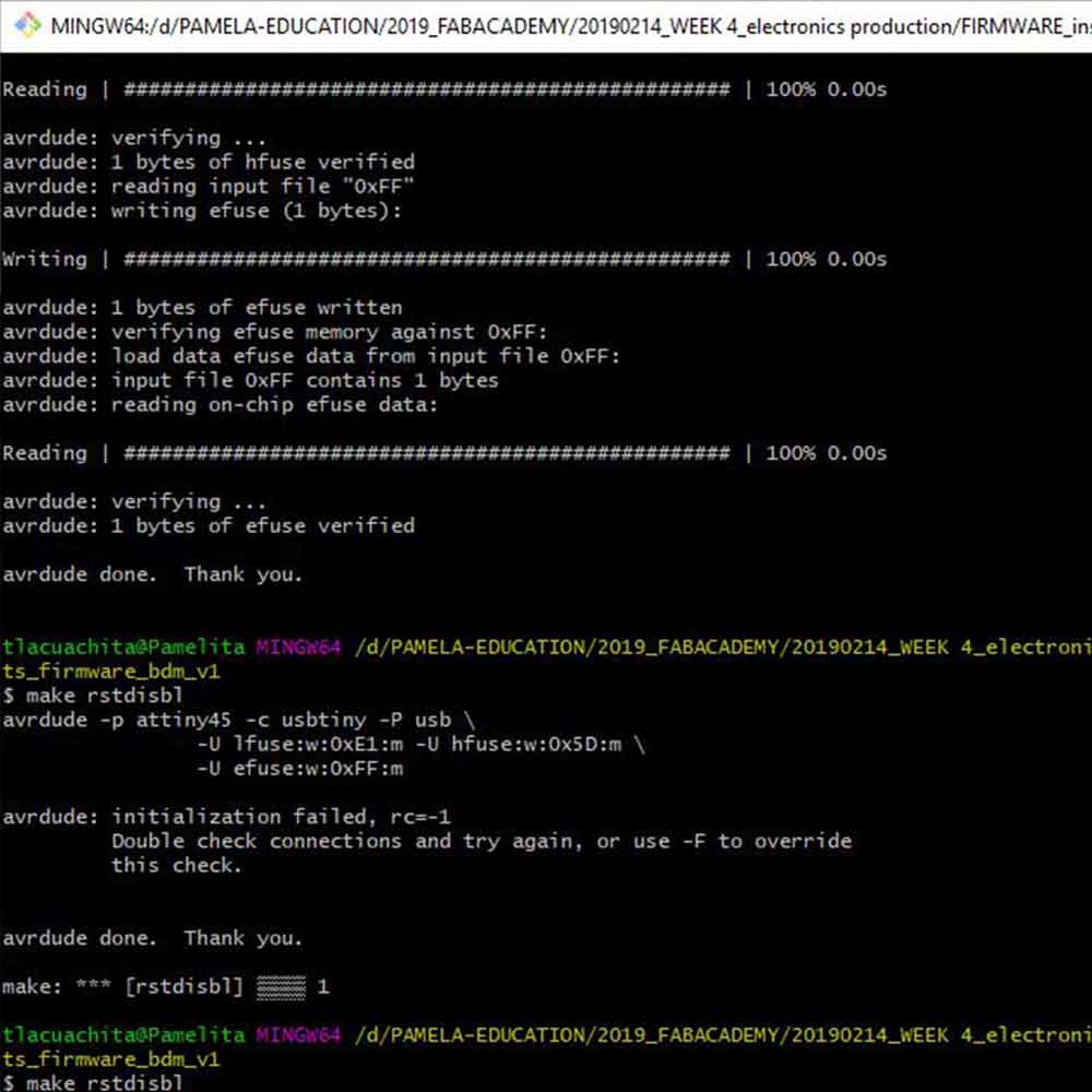
After this you have to run:
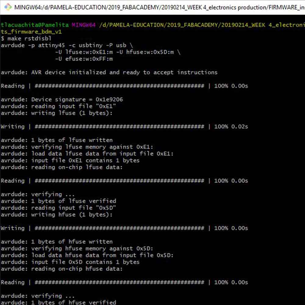
make rstdisbl
But I got this ERROR message :(
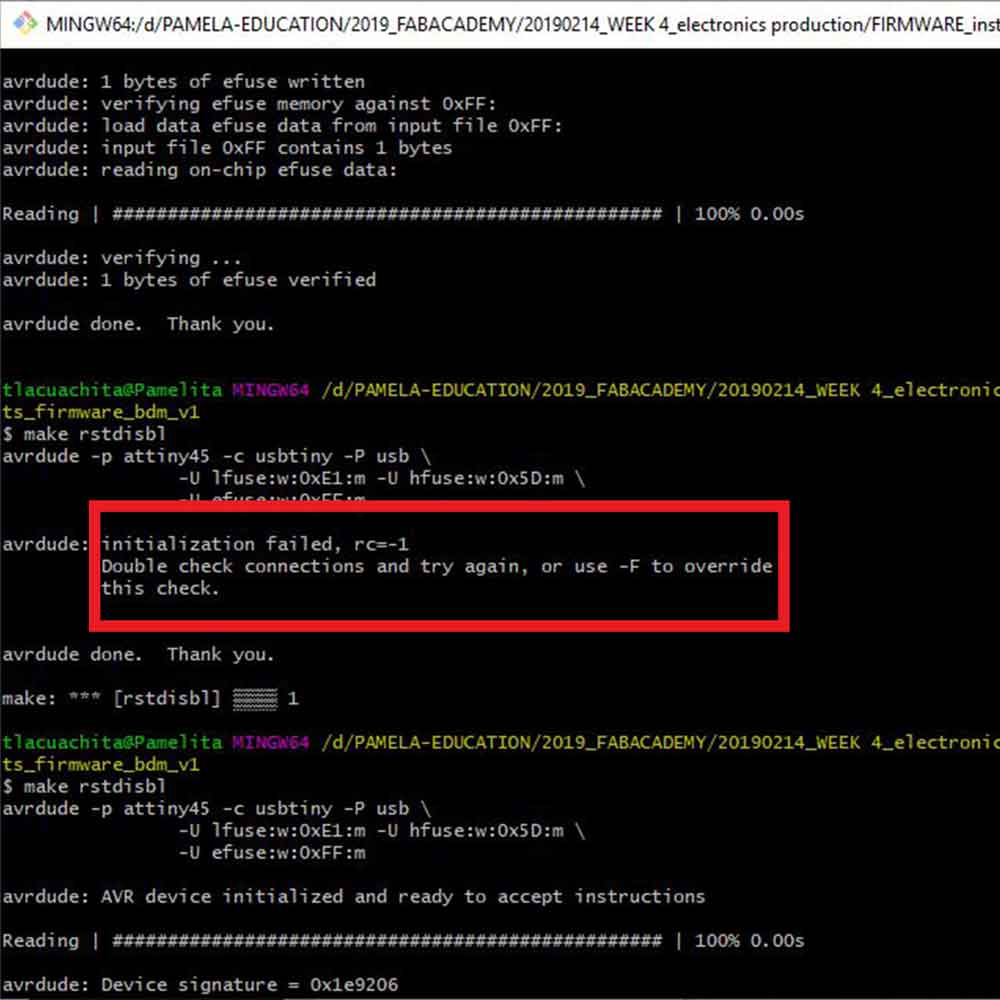
Before you run the command make rstdisbl you have to check that the USB on your new FabIsp is
working and being recognized by your computer. You should unplug and plug once again both FabIsp.
In my case I got the error above as my computer was not recognizing my FabIsp, I just had to disconnect
and reconnect the FabIsp and I checked inside Device Manager if it was detected.
Go to Device manager:
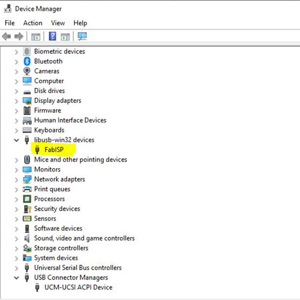
After I made sure it was being recognized, I ran once again make rstdisbl, and this time it worked!
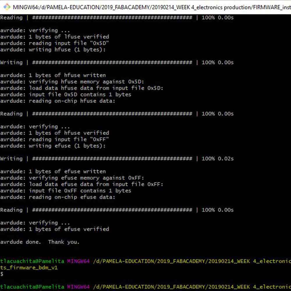
The last step was to desolder the jumper from the board.
This will disconnect the VPROGG from the pin header to the VCC.
Now there's no turn back, I've got a FABISP succesfully programmed!
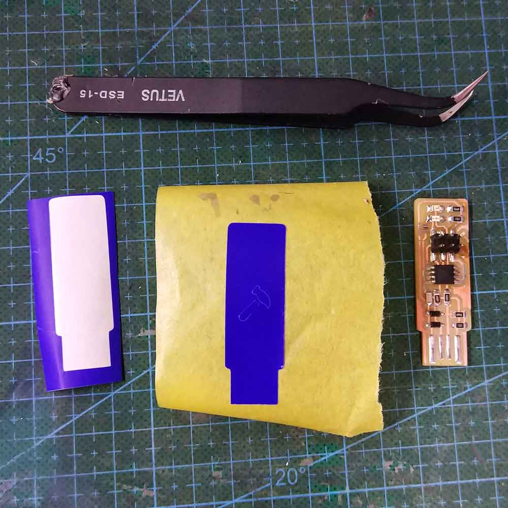
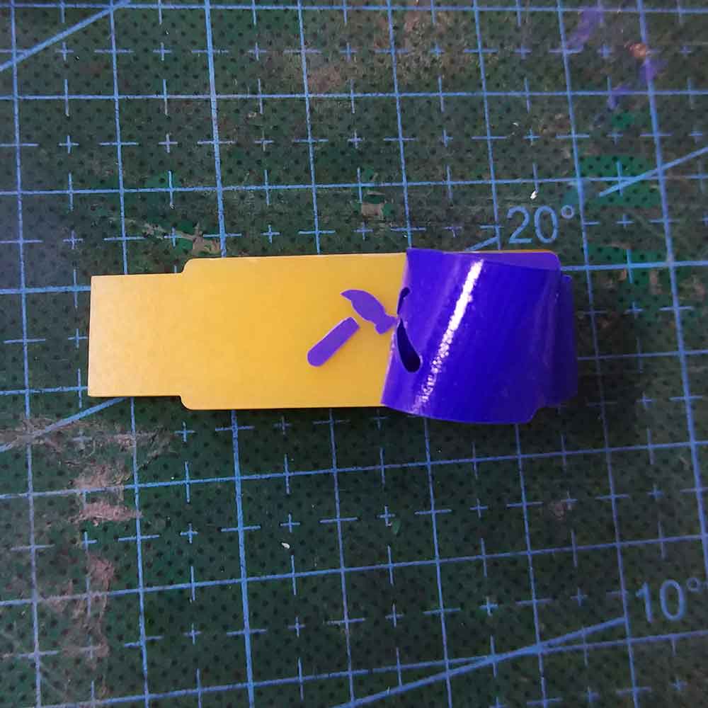
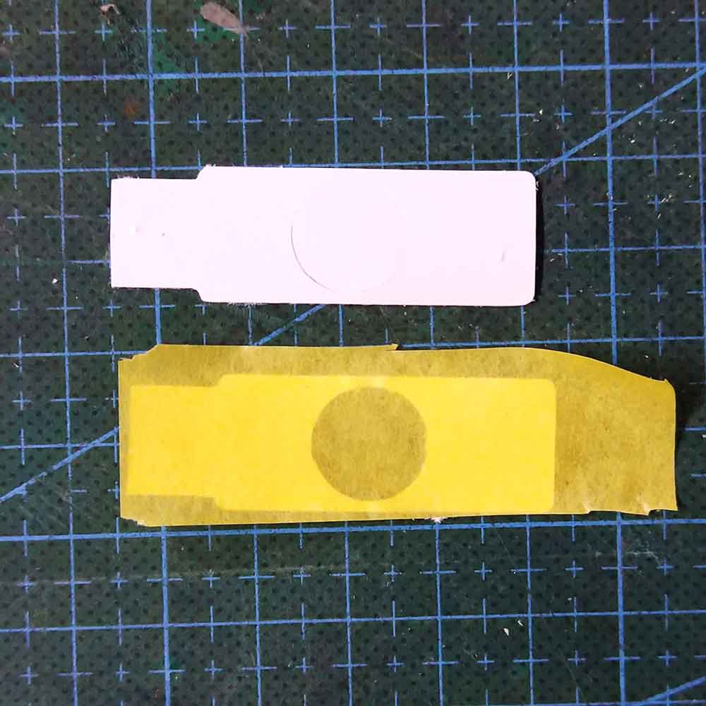
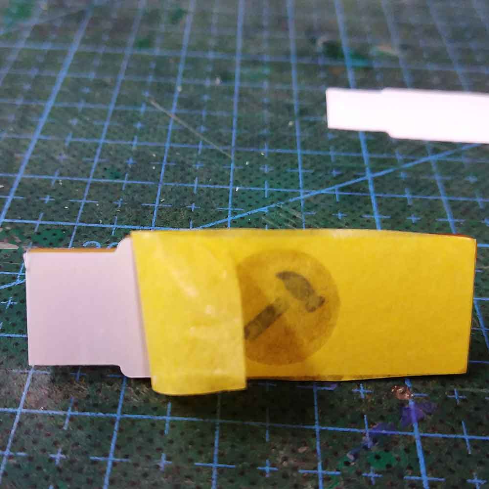
9_VINYL CUT_PERSONALIZING MY FABISP
During last week's assignment we couldn't use the vinyl cutter as it was under maintenance. So I decided to use the vinyl cutter this week and personalize a bit my FABISP:
To read the full documenatation go to (week4_computer controlled cutting)
_DOWNLOAD FILES
Here you can find the files I did on Fusion 360 for the bracelet and the mountains, plus the Illustrator files ready for laser cutting for both files as well: