_week 11
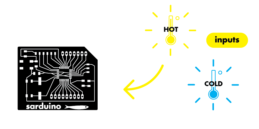
Input devices
Group assignment
This week is about programming a board using input devices and for the group assignment we have to probe
an input device's analog levels and digital signals.
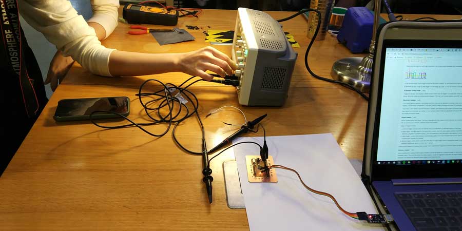
To probe this we will be using an oscilloscope.
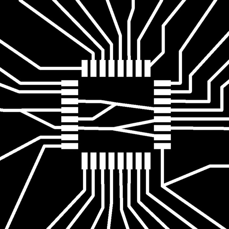
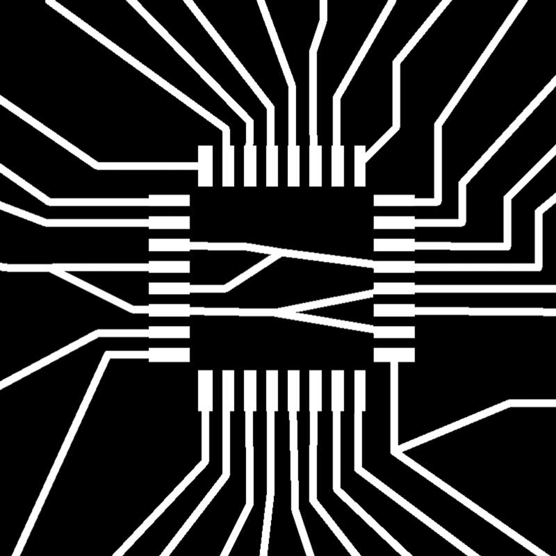
Using the new board of my colleague Flavie we uploaded a blink code to it in Arduino IDE and we used the
oscilloscope to check the digital signal levels that were emitted, in this case ON / OFF = 0 or
5V.
So we connected the alligator clasp to GND and the test probe to SCK where she connected her
LED.
Setting up the oscilloscope and loading the code into the board.
This video shows the digital signals that the LED emits:
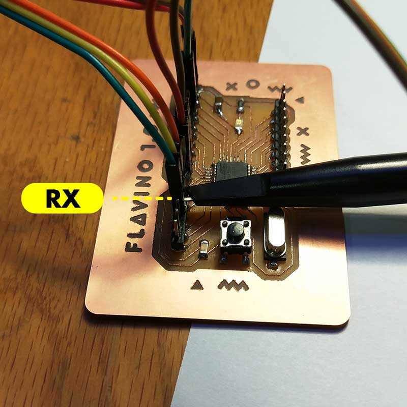
Using the same board we connected an input device, in this case a potentiometer, so that we could read both a digital an analog signal.
How does this work?
If we connect an analog sensor, in this case, a potentiometer, we can read the analog values that the
sensor emits from the pin it is connected from, and the digital values it emits from the serial
communication port (RX).
To do this we used two probes on the oscilliscope, one that connects to GND and to RX on the board this will read the analog signal, and the second probe is connected to GND as well and to the OUT pin on the sensor board.
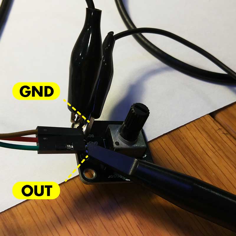
This next video shows the analog signal of the potentiometer. We connected one probe to GND and to OUT pin on the sensor board:
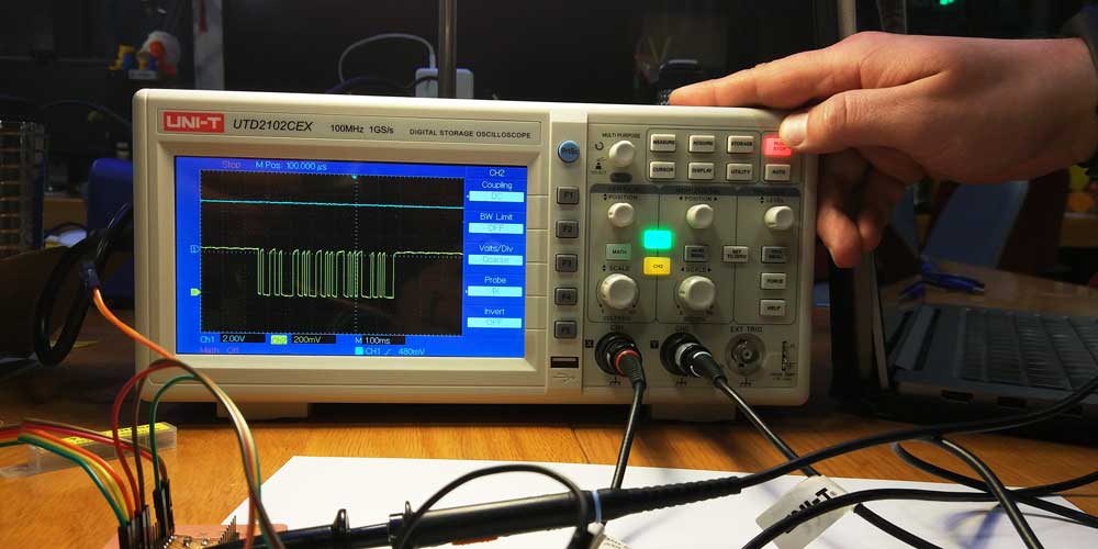
On the following video you will see how we read two values at the same time on the oscilloscope
(analog+digital).
The blue line represents the analog value of the potentiometer, you can see how it increments going up
horizontally. And the yellow lines represents the digital value of the serial communication of the
values emitted (represent 0 or 1).
Individual assignment
This week we have to "measure something: add a sensor to a microcontroller board that you have designed and read it", meaning we will have to design a new MCU and using input devices we will program it to read something.
But, what is an input device?
An input device sends information to a computer system for processing. It can send data to another device, but it cannot receive data from another device. (source from computerhope.com)
For this assginment we could choose a model of an existing MCU from the examples provided, like the FABKIT, which is an Arduino-compatible board based on an ATMEGA328P microcontroller, designed by David Mells or another example we could refer to is the well known SATSHAKIT, which is also an Arduino compatible model based on the FABKIT with several improvements, designed by Daniele Ingrassia.
But why using an Arduino compatible board?
One of the reasons is because we will be using Arduino IDE to program it, so having a compatible board
will help us during the programming phase. Also, as this is a bit more complex than the previous boards
we have done, it is also a nice challenge to try out so we can practice, improve and learn more about
this world of micro controllers.
We were encouraged by our instructor to design our own Arduino compatible board not just to re-do a FabKit or Satshakit. So the following is the documentation of this attempt.
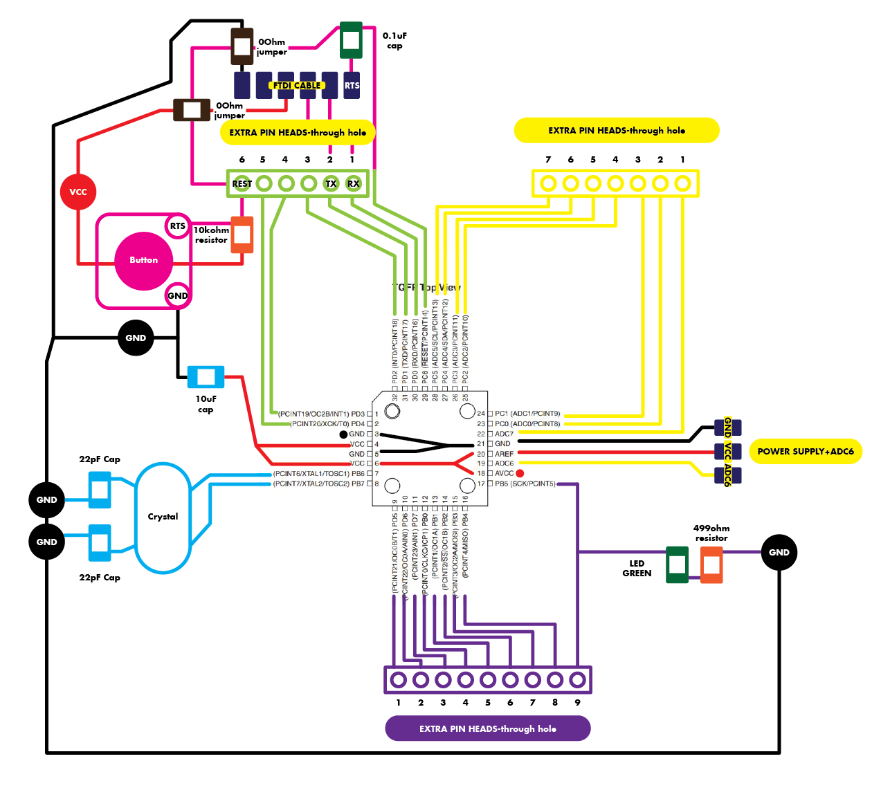
_LIST OF MATERIALS TO BUILD AN ARDUINO COMPATIBLE BOARD
As I am doing an Arduino compatible board, we have to begin by understanding the main components of an
Arduino genuino-UNO board.
During our local lesson, our instructor showed us how to build an Arduino genuino using a breadboard,
which I have to say is useful to understand the components you need and specially to prototype your
idea, but I also have to add I am not a huge fan of building breadboards, I feel there are so many
cables around and they are easy to unplug and to loose the reference of what goes where, but is good if
you use it during a prototyping stage.
To build an Arduino genuino on a board using an ATMEGA328 MCU, you can follow up these two
tutorials
arduino breadboard, tutorial instructables, maker pro
what is important here to
understand is the materials used, as they are going to be the reference for me to build my own
board.
These materials are a base to begin with, and the idea is I can modify/add/remove some
components.
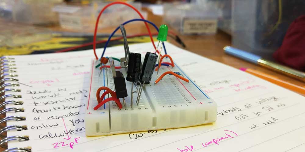
During our local lesson we did the breadboard and tested it using an input device.
I used a temperature sensor as I may need it for my final project.
These are the photos of the breadboard connected and the sensor I added to test an input device.
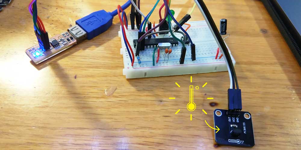
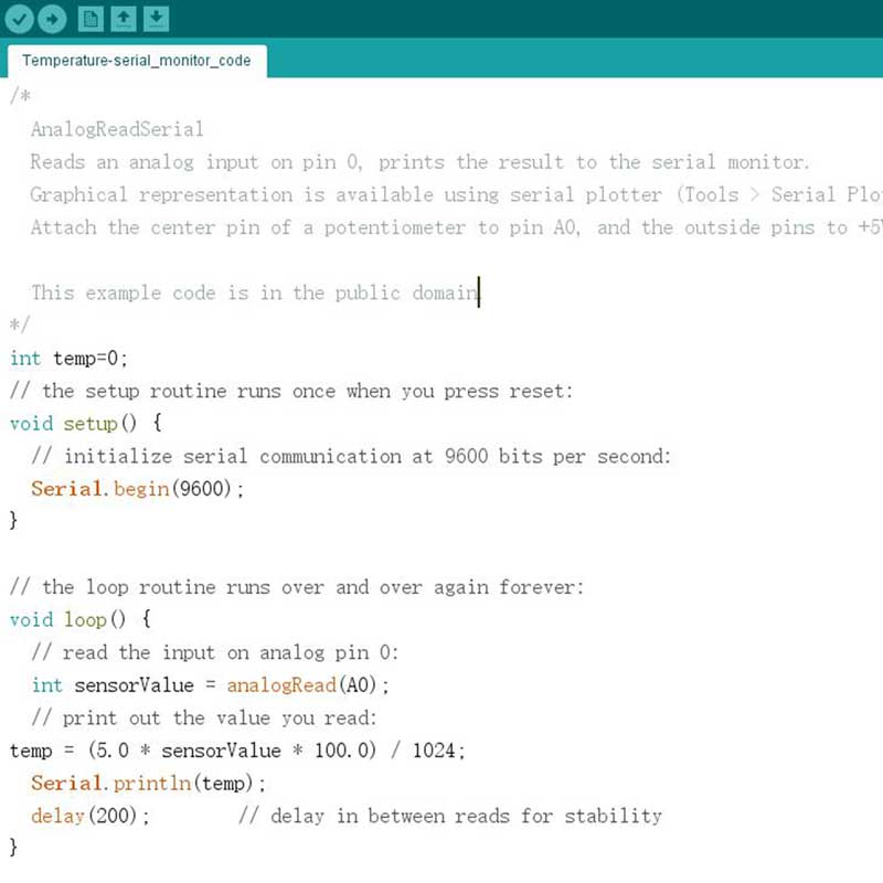
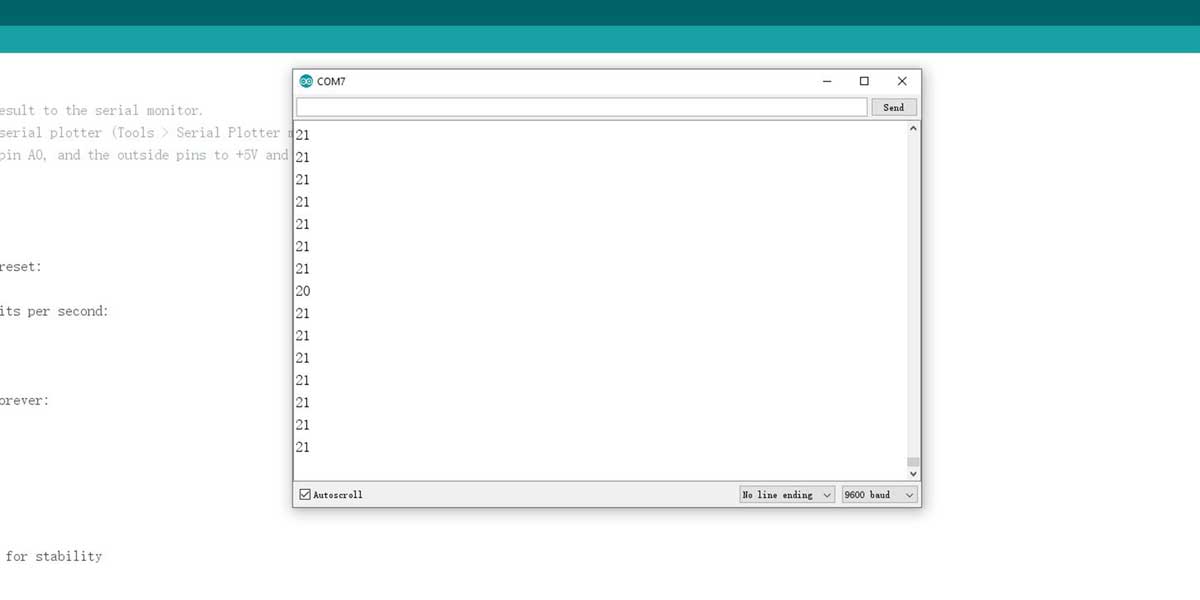
This is the code I used to upload into my breadboard to read the temperature values.
As I said is practical to do a quick prototype of your board in a breadboard.
I decided I wanted to base my new mcu on this famous SATSHAKIT so I first took a look to the
documentation available and I tried to understand what components he used and what they are for.
It took me a little to understand and to figure out the world begind the Satshakit.
So the first thing I did was a comparison list of the components an arduino genuino-uno uses and the
components of the Satshakit.
This helped me to better understand what I could add/remove for my own board.
_UDERSTANDING SATSHAKIT
As the Satshakit was my refrence, before I started my own board schematic on Eagle I wanted to understand
a bit more the components he used.
There are a few components that it took me a bit to understand why they were there:
1_For example, if you check the schematic you will notice that the pin heads none of them are an FTDI
group connector, so if you need to connect an FTDI cable you will need to connect cables separately in
different pin heads.
2_There are two pins specially dedicated to VCC and GND as there is no GND or VCC on the other pins.
3_There are several capacitors, one of 10uF which is used as a decoupling capacitor (to supress
voltage spikes) and you should have it on your board, never forgt it (I did...). But there are also
another three more capacitors one of 1uF and two 100nF, these are also decoupling capacitors
which their design and usage is a bit more advanced for what I need on my board, so I could ommit these
three.
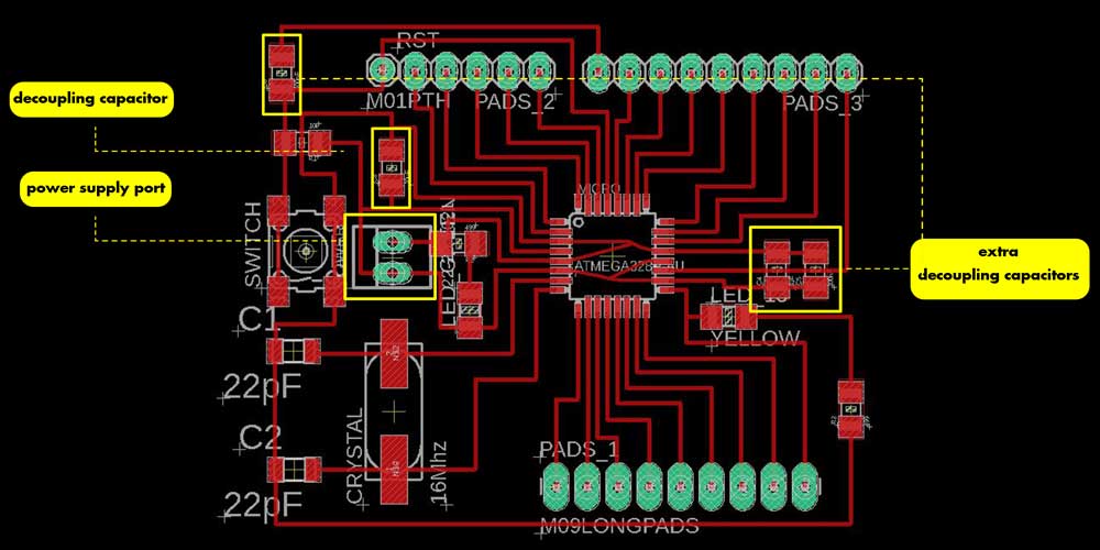
So my first iteration of board included the following components (note that I made a mistake ommiting the
10uF capacitor and there are some mistakes on the connection between the 01uF capacitor and RST):
_ATMEGA328
_One switch/button with a 10kOhm resistor
_one 0.1uF capacitor between RST (on the ATMEGA328 pin) and the RTS on the FTDI pin header
_one crystal with two 22pF capacitors ("The capacitors are there to resonate with the crystal
inductance and cause the crystal to oscillate on its fundamental parallel-resonant mode."-source
quora.com)
_I originally thought of adding two extra capacitors for decoupling one of 1uF and one of 100nF, but on
the second iteration I removed it.
_one LED with its resistor (499 ohm)
_pin headers: my original design had 3 sets of pin headers but I had no FTDI pin header group
This was the initial list of my compoents but I will explain what and why I changed a few things later.
A colleague did a sketch of where she would place her components and I thought this was very useful to have a general idea for the connections, so to have a better understanding of it I did a graphic map of where to place the components:
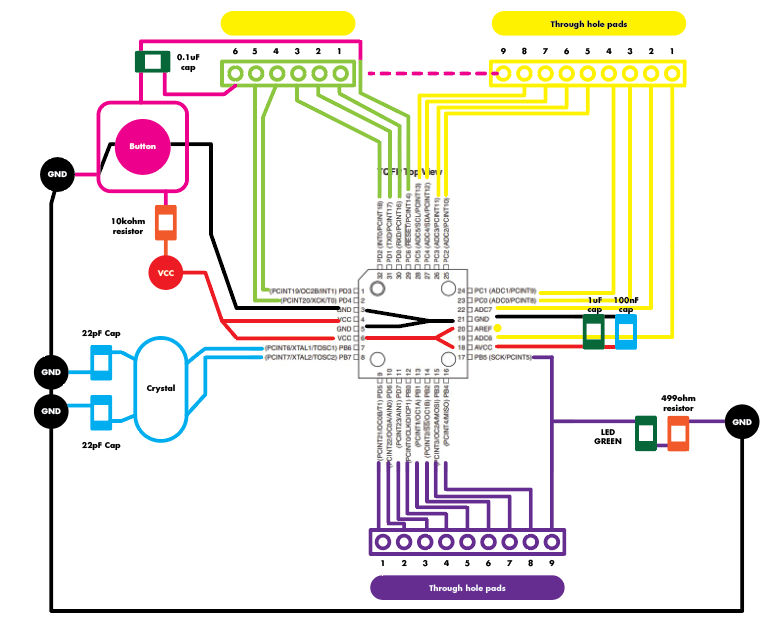
Once I had my list of components and diagram of where I would place my components I started doing my schematic on Eagle.
_BUILDING MY BOARD
Many of the components that I used for this board are not inside the FAB library, so I had to download
several libraries for several components.
Here are the links:
_ATMEL328 component, be
careful when adding this component, as there are different models and we noticed that some where even
smaller, so a good advise is that once you add your component check on your board the size of it and
compare it to your ATMEGA328 chip.
_Pin heads 1
, Pin heads 2
I used through
hole components so I needed some new libraries for them. Also here be extra careful and make sure you
don't use very small pads, always check the sizes.
_Voltage regulators
, be careful when
adding this component, as there are different models and we noticed that some where even smaller, so a
good advise is that once you add your component check on your board the size of it and compare it to
your ATMEGA328 chip.
_Crystal and resonator libraries, I am using the model CSM-7X-DU (Version 1)
Note: Remember that this are pads, if you can't find a component you can create your own from scratch of
modify an existing one, as you just need the footprint when you save the .PNG.
To change the footprint design you have to go inside properties and there you can modify the sizes.
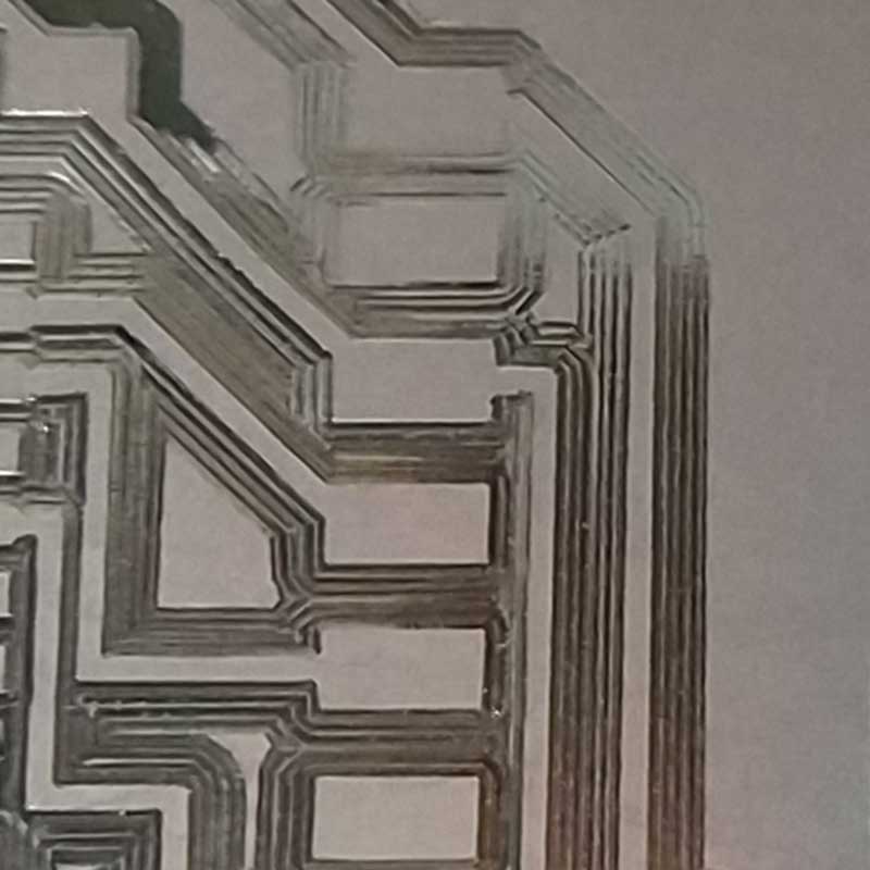
I was using Satshakit as a reference and I followed as well the settings they used for the design rules, instead of the FAB DRC which was a mistake as the traces where too small and you will see later the final result.
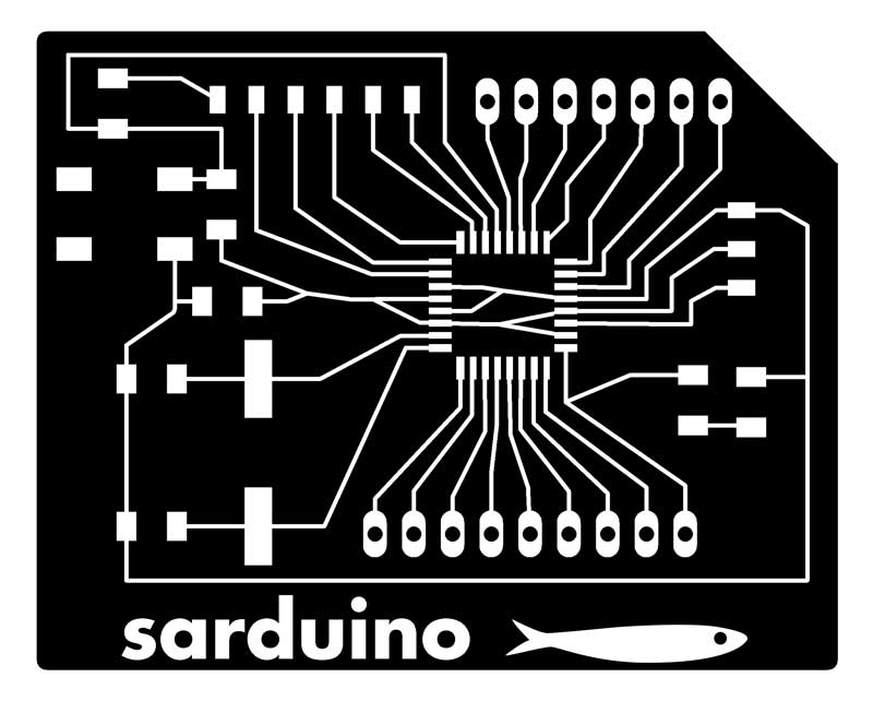
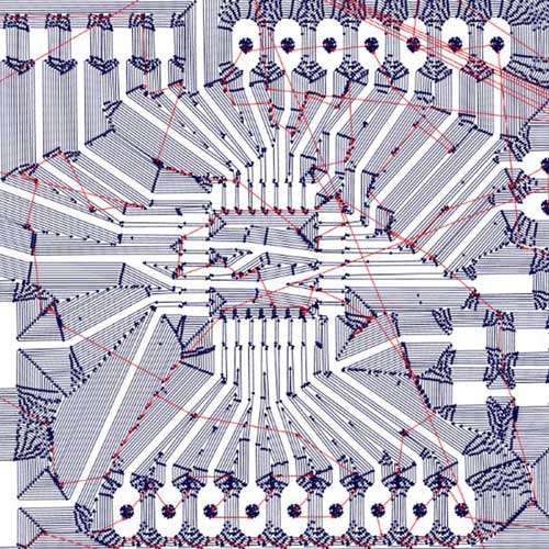
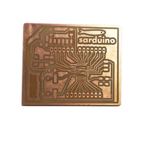
The first board I did was looking like this:
When I opened the file on FabModules to do the traces task the space between the ATMEGA legs is so narrow that using our diameter tool of 0.4mm it couldn't get through, so I had to add some extra spacing between the legs in Photoshop. I just added some extra black rectangles in between the legs.
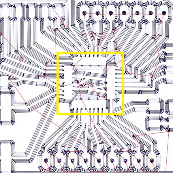
The left image below is the original traces file generated from Eagle, the image on the right is after adding extra spacing in Photoshop.
While working on the traces as me and another colleague were using Satshakit design rules, we realized that if we set up the diameter tool to 0.4mm we still had issued in between some traces, so we tried decreasing the value to 0.3mm:
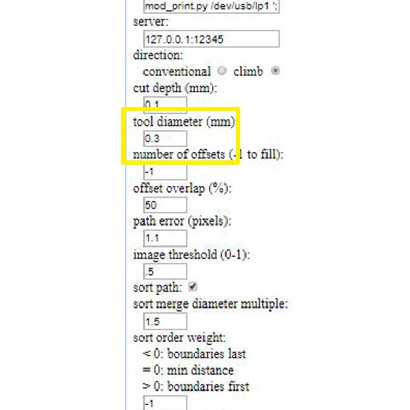
This way we were able to reach all the areas when milling the board.
_ERRORS & ADVISES
This week was a bit (VERY) hard for me, I struggled at the beginning when building my board, I had a lot of confusion and doubts when doing the schematic as I was trying to use as reference the Satshakit which is a complex jump for me. It took me 2 and a half days and 8 avergare hours of sleep, to have my first schematic ready. What helped me a lot was drawing a diagram to understand the connections, also while working in the lab during the weekend between me and another colleague Flavie we helped each other and tried to solve our doubts we had when building the schematic. I find it useful and important to share your work with your peers, commnicate with them and try to help each other, as sometimes our tunner vision won't take us anywhere, and if they have similar problems/errors you realize you are not the only one lost and you could try solving it together.
Another advise for this board and next ones, USE THE FAB DRC RULES DON'T TRY TO OVERRIDE THEM. Several colleagues and me we decided to use Satshakit DRC settings, the problem about doing this is that the traces were too thin and we were not using thecorrect spacing in beetween the traces from the FAB DRC so the result was a board with very thin traces.
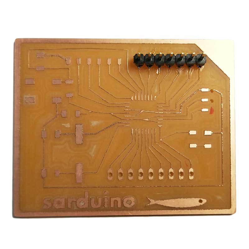
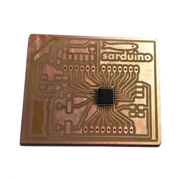
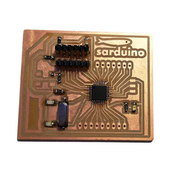
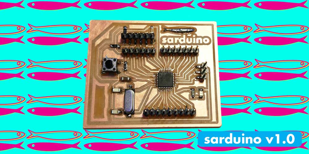
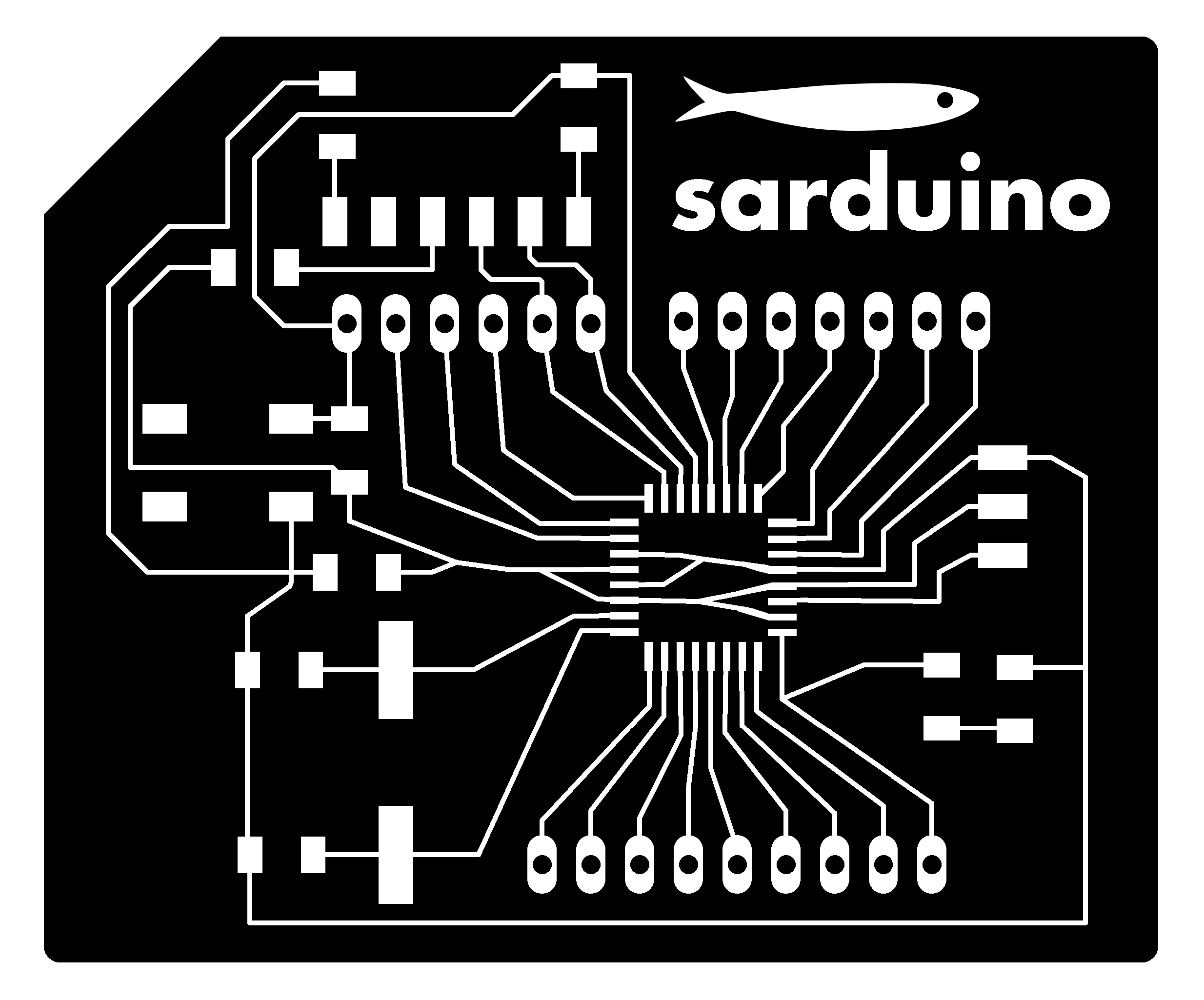
_SARDUINO v 1.0
I baptized my board SARDUINO
This is the first board I milled and I had a few issues while doing the milling process...
_ERRORS
After the traces task was done during the milling process, many parts of the surface didn't cut through the copper layer, so I ran the task 2 more times and I changed the endmill twice, but the copper it didn't remove the copper on those areas. I forgot to take a photo of how my board was looking, but that day I spent until 4am at the lab and my brain was disconnected from reality, but I do have a photo from the electronics design week where I had a smiliar error and the surface of my board was looking like this:
As I already ran the traces task twice and nothing happen, I thought about changing the file in FabModules and I lowered the CUT DEPTH to 0.2mm
Some notes I would like to add here to avoid this type of issue next time is:
1_If you reuse a FR1 sheet, make sure is flat before you place it on the sacrificial layer.
2_Make sure whenn you place your stock on the sacrificial layer that is perfectly flat.
3_If you use the NUMBER OF OFFSETS in -1 now that the task will take a looooong time as
you are removing almost all the copper on the sides, and you are also consuming a lot the tip of the
endmill. So stick to 4 offsets if you want to avoid a long wait and bad endmills.
I managed to finish my board at almost 5am and I wisely decided to solder the components the next day after howing the board to my instructor to get his feedback.
This was a good idea because this first board I designed had several issues:
1_The traces were very thin (0.4mm thick)
2_I forgot to add my 10uF decoupling capacitor
3_I didn't put an FTDI pin group which is something I new I was doing from the beginning but I didn't
realize how impractical this would be when doing connections.
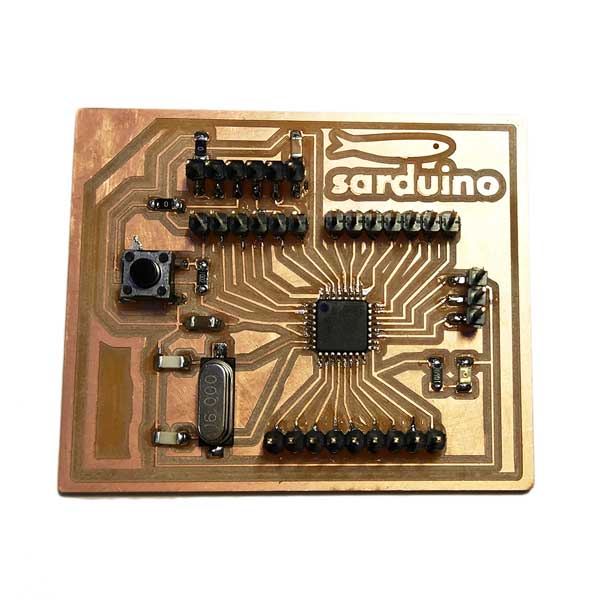
So I modify my file on EAGLE and milled a second board.Here is the schematic of the new connections and components:
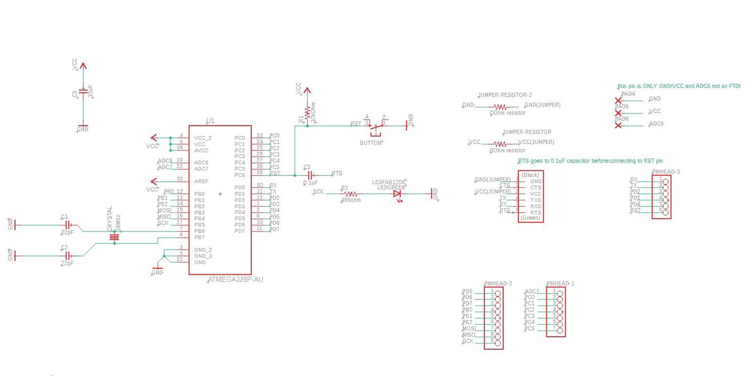
I added one FTDI group of pin headers, the 10uF decoupling capacitor (CONTROLS THE VOLTAGE SPIKES-TO PLACE AS CLOSE AS POSSIBLE TO THE MCU)I forgot and as I added the new FTDI and I needed VCC and GND and it was difficult to re arrange the in in another place, I added two jumpers to jump to get VCC and GND.
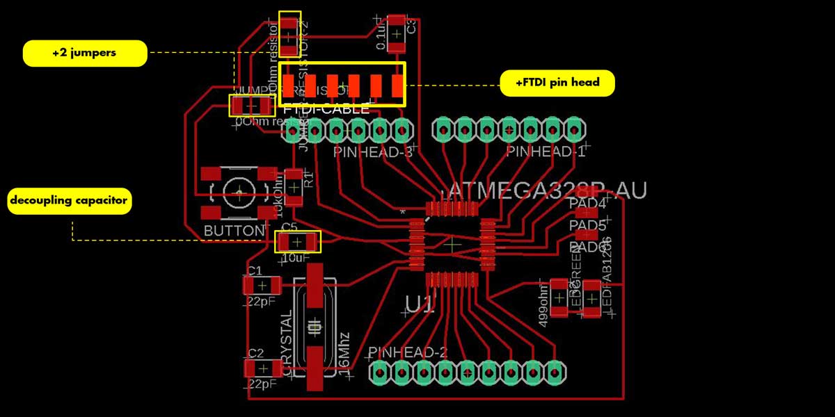
I redraw my diagram with the new modifications, so I could better understand the connections before doin it on Eagle.
Once I had my EAGLE file ready I prepared 3 .PNG files to import into FabModules, one for the traces and two for the outlines (one for the holes as I added through hole components pin headers) and one for the outer shape, but I could have saved this two outlines in one single file to run only one outlines task.


The scond milling came out pretty good, then for the soldering part I thought it would be really hard to
solder the AtMega328 as the legs are very thin and small, but what I did was to apply first some
soldering in two legs on opposite sides, then once fixed I put soldering to all the legs and I removed
the excess with the desoldering braid.
Here are the photos of the milling result and the soldering:
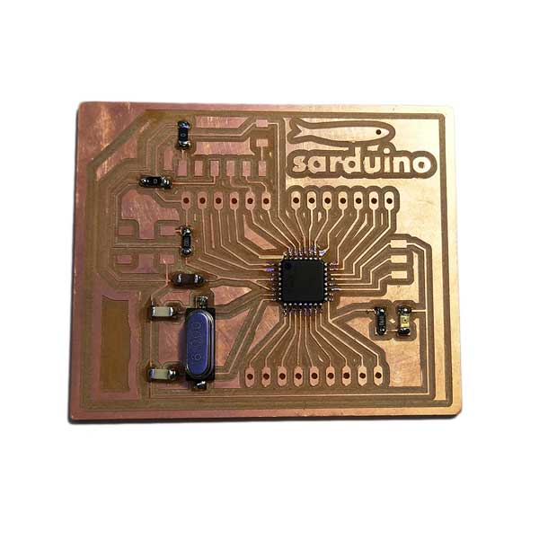
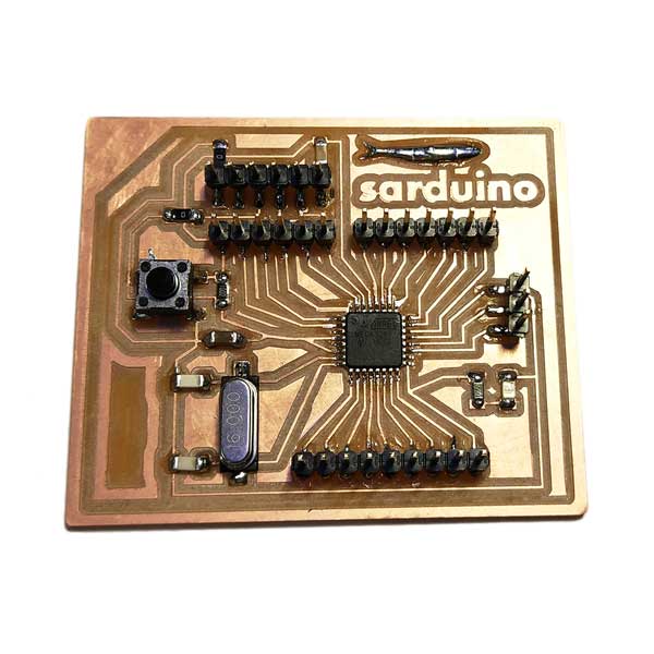
And here is the first Sarduino soldered and ready to try and be programmed!!!
_PROGRAMMING ARDUINO WITH INPUT DEVICES
Up until now I think I used 80% of all my available time to complete this task, doing the board from scratch following the Satshakit as an example took me a long long time. So I just had one day more to try programming it, and... it was not that simple at the beginning for me.
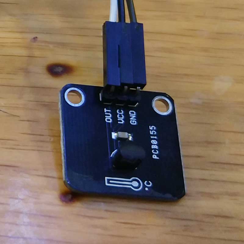
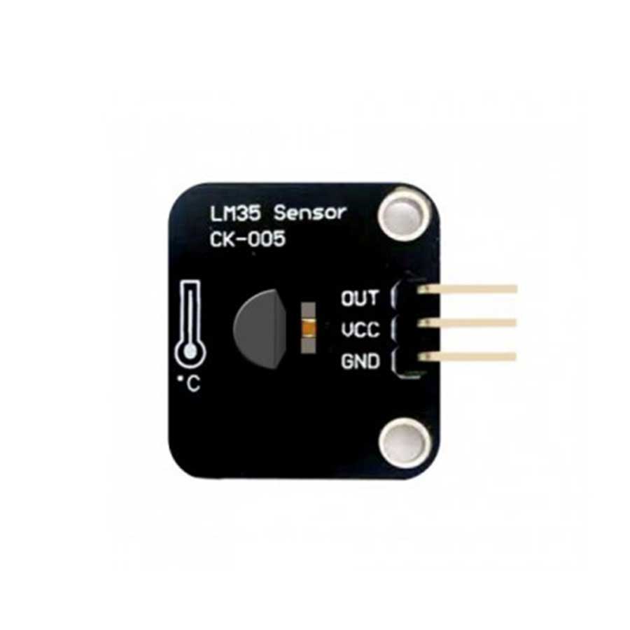
To program my board I decided to use a temperature sensor as my input.
_TEMPERATURE SENSOR INFORMATION
The type of temperature sensor I will be using is a LM35 temperature sensor, it has 3 pins to connect, one forVCC, GND and OUT. OUT has to be connected to an analog pin as we are reading analog values, so for this example I connected it to pin AO (for arduino) or PC0 on the ATMEGA328 pinout.
This sensor is calibrated in Celsius and can read values that range from -55℃ to 150℃. It works
with 4V up to 20V.
The sensor can come in different packages the one I am using comes as an LP packed pin:
Here you can find the data sheet of the sensor I will be using _LM35 temp sensor
._RUNNING THE CODE
To start coding you can try first lookig for codes available online, but make sure the code is the correct one for the sensor you are using. You need to convert the voltage to Celsius degrees, and normally you will find this formula on the sensor data sheet.
In our case the formula to add into the code is this one:
temp = (5.0 * sensorPin * 100.0) / 1024;
Here you can find two nice tutorials well explained, on how to use a temperature sensor this one uses a model TMP36 tutorial, and this one from sparkfun.
So once I had both the formula and figured out the sketch, I connected my board with the FTDI cable, as the ATMEGA328 I soldered had previously been burnt the bootloader so I didn't need to use the FABISP to program it. But...
_ERROR WITH MY FTDI CONNECTION
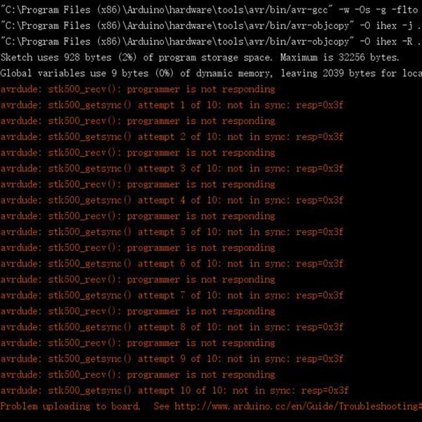
So, this message is related to connections problems, so I tried reconnecting the FTDI switching RX,
Tx positions, checking continuity with the voltimeter, but nothing... my FTDI doesn't
work, but at this point I needed to complete the assignment and I decided to use my FABISP instead to
load the code into my board, unfortunately I wouldn't be able to use serial monitori to read the
temperature values on my computer, so assisted by my instructor I wrote a code where the increasement or
decreasement of the temperatur would turn on or off the LED on my board.
This is the code I used:
int ledPin=13;
int sensorPin=A0;
int temp=0;
void setup() {
// put your setup code here, to run once:
pinMode (ledPin, OUTPUT);
}
void loop() {
// read the value on sensorPin
int sensorPin = analogRead(A0);
temp = (5.0 * sensorPin * 100.0) / 1024; //formula to convert voltage into Celsius degrees
if(temp>=18)//if temperature is equal or bigger than 18 degrees
{
digitalWrite(ledPin,HIGH);//Turn ON LED (as my serial monitor doesn't work I turn on/of the LED)
}
else//if temperature is under 19 degrees
{
digitalWrite(ledPin,LOW);//Turn OFF LED
}
}
You can see I added the formula to convert the analog value into Celsius and a simple variable using if and else to turn on and off the LED lights.
Here is a video of the sensor working:
_USING A POTENTIOMETER
During week 12 of output devices I used a potentiometer together with a servo motor as an exercise.
You can find the documentation inside week 12 output devices of using this
module.
_CONCLUSIONS AND IMPROVEMENTS
This was one of the hardest week for me so far, it's been a challenge creating the board and now having issues with the FTDI makes me even more eager to keep trying and learning what could be the error, how to solve and how to improve the design of my board.
I plan next week to redo a new Sarduino V2.0 improving the connections, taking more care when soldering and understand what could the the issue.
Even though it would have been better to have the serial monitor to use this specific sensor, it is also nice to learn other ways to read an input, like in this case turning on and off an LED, so whenever I find in this situation, there is always room to try out and then of course to improve.
_CODES DOWNLOADS
_LED on/off reading temp value