The task for the week was to make an In System programmer for programming microcontrollers. So let understand about the same and how it could be made
In System Programming
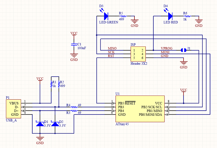
In-System Programming (ISP) is programming the microcontroller while the chip is on board and connected to many other components . During ISP every pin on microcontroller is disabled and chip is programmed by means of a programmer which follows some protocol.Chip removal is not necessary during programming. The ISP circuit used by me for the time was
'FabTinyISP'
FabtinyISP
The FabTinyISP is yet another version of an AVR ISP programmer/board that can be produced in a fab lab using a milled PCB and readily available components.The complete details of this ISP is available 'here'
.
.
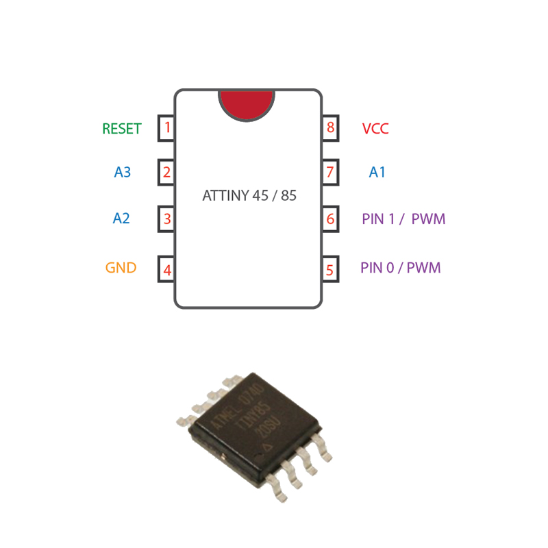
The major component ie, the microcontroller used in this ISP is attiny45
.
Attiny 45
The microcontroller that is using in FabTinyISP is Attiny 45. Attiny45 is a High perfomance and low power 8- bit AVR microcontroller running on RISC Architecture by Atmel (microchip acqured Atmel recently). Attiny 45 comes in a 8 pin package. Attiny 45 have 6 I/O pins, Three of them are ADC pins (10 bit ADC) and other two are Digital pins supporting PWM.It comes with a 4KM flash memory, 256 In-System Programmable EEPROM and 256B SRAM. Operating voltage around 1.8V to 5.5v 300mA. Attiny 45 support Universal Serial Interface. Both SMD version and THT versions are available in the market. Attiny 85 is a higher version of Attiny 45, They are almost same. Tghe only difference is in the Flash memory, Attiny 45 have 4KB flash and Attiny 85 have 8KB flash. We can choose either Attiny 45 or Attiny 85, Not a big deal but Attiny 45 is more enough to make FabTinyISP. In fablab we have SMD version of Attiny 45 is available. See the official documentation from here.
ATtiny 45 : 4KB FLASH /256 B EEPROM / 256 B SRAM
ATtiny 85 : 8KB FLASH / 512B EEPROM / 512 B SRAM
- Special Features :-
- debugWIRE On-chip Debug System
- In-System Programmable via SPI Port
- External and Internal Interrupt Sources
- Low Power Idle, ADC Noise Reduction, and Power-down Modes
- Enhanced Power-on Reset Circuit
- Programmable Brown-out Detection Circuit
- Internal Calibrated Oscillator
.
.
I have basic experience in PCB creation using the etching process, but using a milling tool was a whole new experience
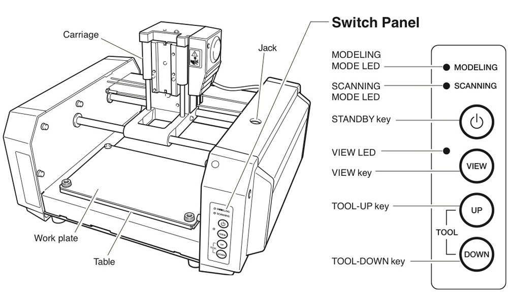
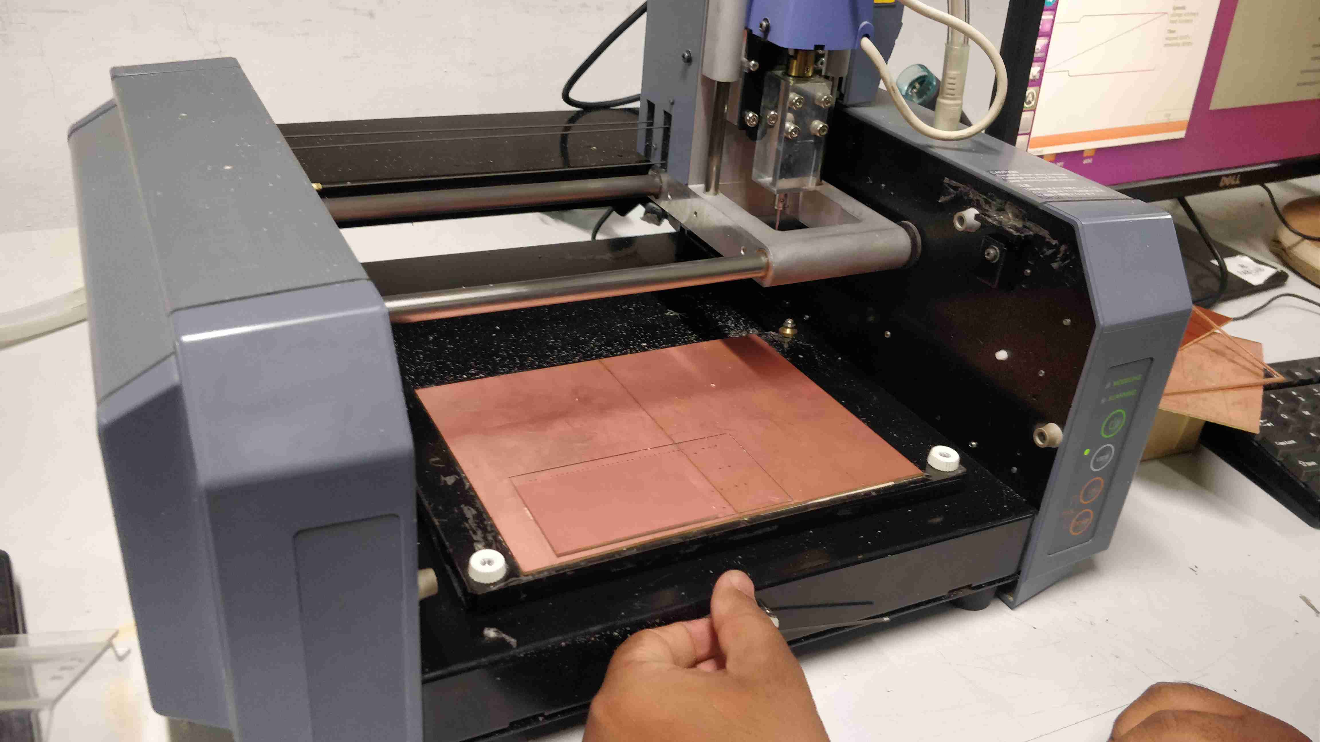
Roland Modela MDX20- Milling machine
.
The Roland Modela MDX-20 is a small milling machine and a 2 1/2D precision scanner.
This machine is mostly used for milling circuit boards, though it can also mill in other soft materials like machinable wax. For milling circuit boards you should export you design into a black & white monochrome png. The second use of this machine is scanning. It uses a thin needle to gently touch the object and calculates from this a 2 and a half dimensional model. Though slow at processing, it can create a high detailed model.
.
.
Tracing and milling
.
.
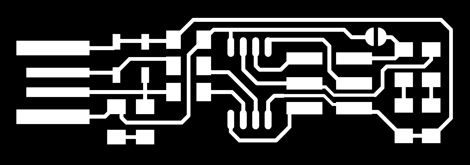
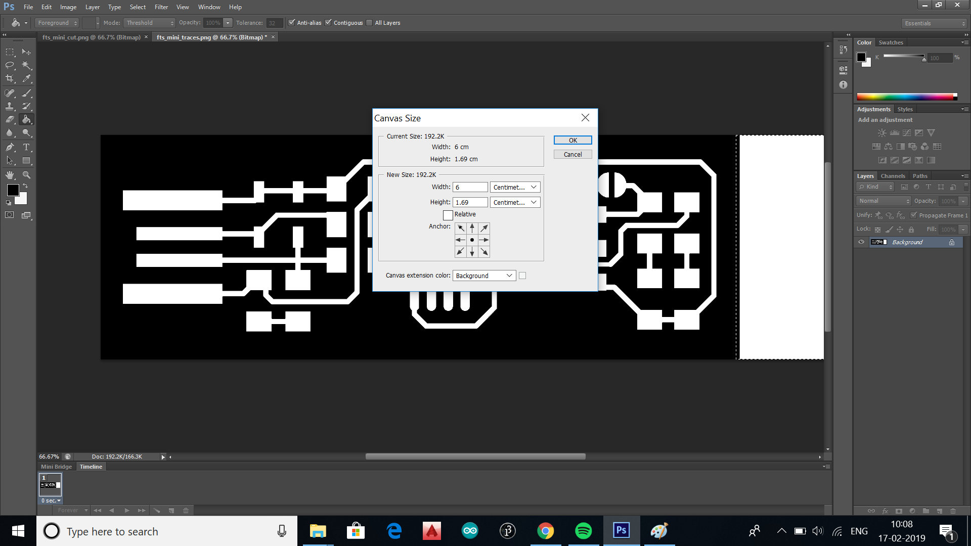
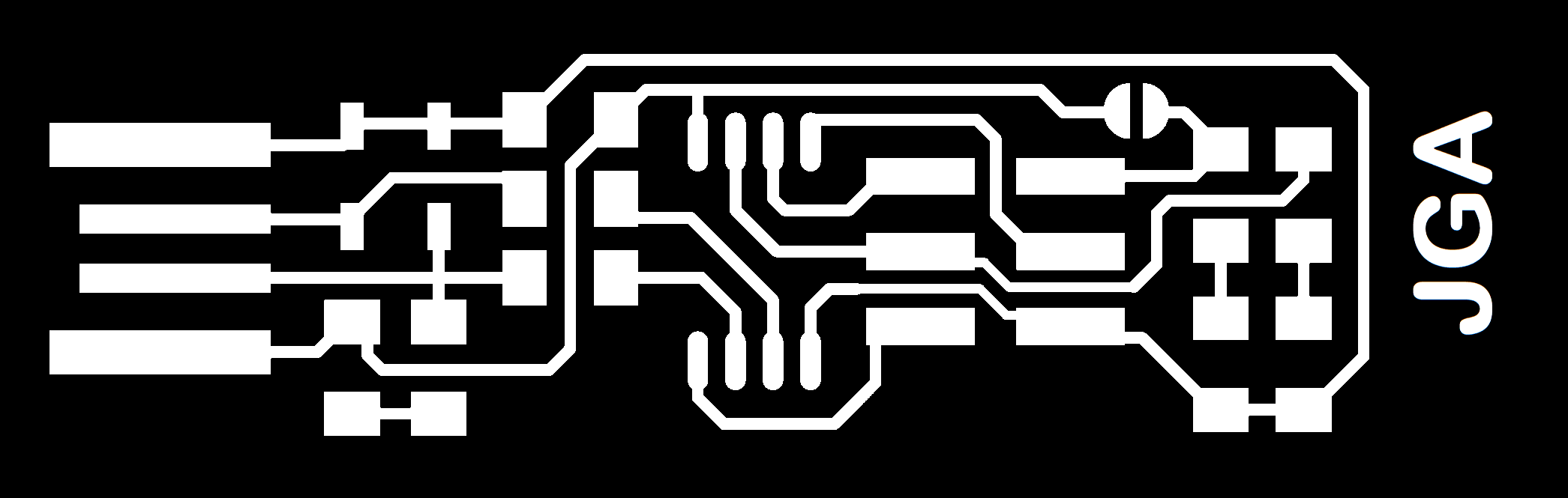
The png file for milling and tracing the PCB was downloaded. In order to differentiate from other boards , i thought i would add my name in the bottom and respective changes were made on the png files using photoshop and below images were obtained.
.
.
Files for tracing and milling
.
.
DOWNLOAD FILE 1
.

.
DOWNLOAD FILE 2
.
Let's start milling
.
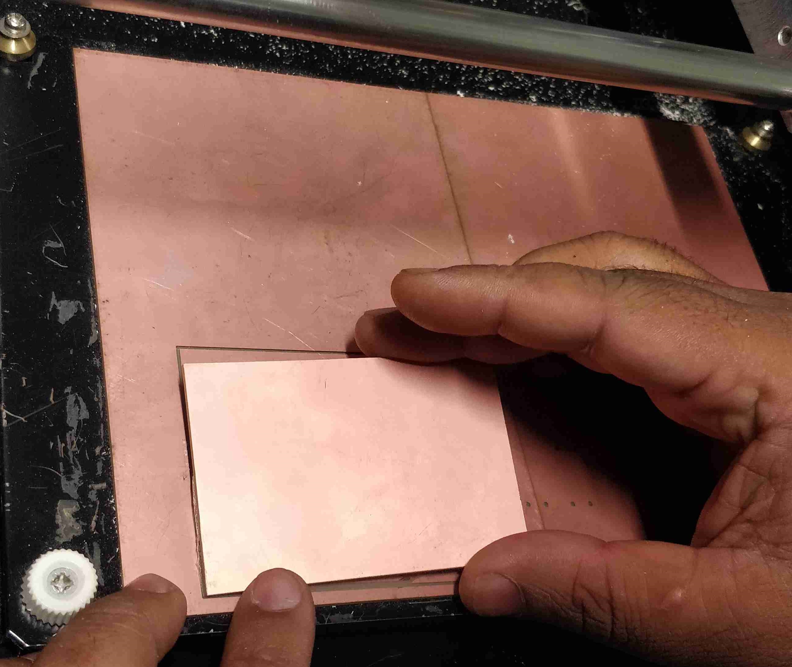
- Setting the sacrifical Layer: Inorder to protect the bed from getting damaged during milling a sacrifical layer is used, here a spare PCB is glued to the bed near to origin position (x,y;0,0) and above that we will be placing the PCB for milling. Press 'View' button to keep the machine in view mode inorder to work on the Miller Bed
.
.
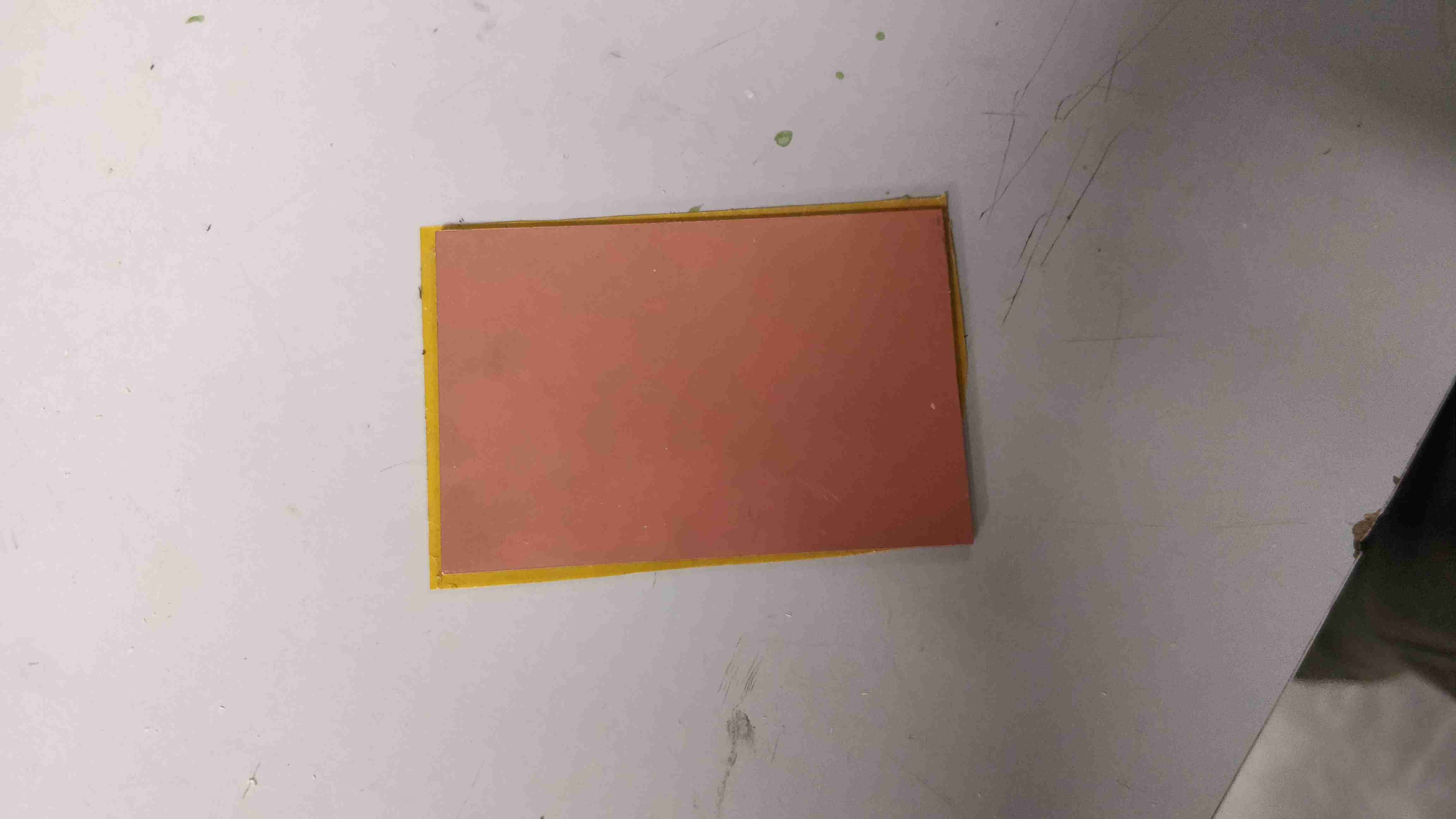
- Cutting the PCB and placing it on sacrificial layer: Keeping the machine in view mode, the PCB with the required size is placed in the sacrificial layer close to the origin position (x,y;0,0).Here we are using FR-1 Grade PCB,since we only need one layer and is cheap and easy to mill. Double side tape is used to stick the PCB to the sacrificial layer so that it removable in future
.
NOTE : Different types of PCB
- FR1-FR4
- FR1 is basically the same as FR2. FR1 has a higher TG of 130 Celsius instead of 105 Celsius for FR2. Some laminate manufacturers who produce FR1 may not produce FR2 since the cost and usage are similar and it is not cost effective for having both.
- FR3 is also basically FR2. But instead of phenolic resin it uses an epoxy resin binder.
- FR4 (FR = Flame Retardent)is a glass fiber epoxy laminate. It is the most commonly used PCB material. 1.60 mm (0.062inch). FR4 uses 8 layers glass fiber material. The maximum ambient temperature is between 120o and 130oC, depending on thickness.
In China FR4 is the most widely used PCB base material, next is FR1 then FR2. But FR1 and FR2 are usually used for 1-layer PCBs because they are not good for passing through holes. FR3 is not recommended to bu ilding multi-layer PCBs. FR4 is the best selection. FR4 is widely used because it is good to make from one- layer to multi-layer PCBs. With only FR4, PCB companies can make all kinds of PCBs, which leaves the management and quality control much easier, and eventually it can reduce the cost!
- CEM-1 and CEM -3
- CEM-1 Composite material composed of woven glass fabric surfaces and paper core combined with epoxy resin. Primarily used in the printed circuit board industry. Easy punching and excellent electrical properties and higher flexural strength than paper based grades. CEM-1 provides excellent mechanical and electrical properties, and punches well up to .093″.
- CEM-3 is very similar to FR4. Instead of woven glass fabric a ‘flies’ type is used. CEM-3 has a milky white color and is very smooth. It is a complete replacement for FR4 and has a very large market share in Asia. It is a kind of flame retardant epoxy copper-clad plate glass material, is generally used in electronics with double sided and multilayer pcb boards. And CEM – 3 is a new printed circuit substrate material developed based on FR – 4. In recent years, CEM-3 is used to replace FR-4 in Japan, even more than the FR – 4 dosage.
- Aluminum Metal Core
- As Aluminum Metal Core PCB means the base material for PCB is metal, but not normal FR4/CEM1-3, etc, and currently what the metal used are Aluminum, Copper alloy. Aluminum Metal Core PCB are used instead of traditional FR4 or CEM3 PCBs because of the ability to efficiently dissipate heat away from the components. This is achieved by using a Thermally Conductive Dielectric Layer.
- Flex and Rigid-flex
Flex and Rigid-flex circuit boards have become increasing popular due to their unique applications. Flex and Rigid-flex circuit boards can do what regular standard rigid circuit boards can not do. They can fold, twist, and wrap around tight/small packaging area.
Most flex circuit boards are being manufactured using “Kapton”, a material developed by Dupont Corporation. This polyimide film based material is resistant to heat, has dimensional stability and a low dielectric constant of 3.6. There are three variants of the Kapton material:
-
1. Pyralux LF (Acrylic Base Adhesive-not Flame Retardant)
- 2. Pyralux FR (Acrylic Base Adhesive-Flame Retardant)
- 3. Pyralux AP (Adhesiveless-for more Demanding high-performance applications)
.
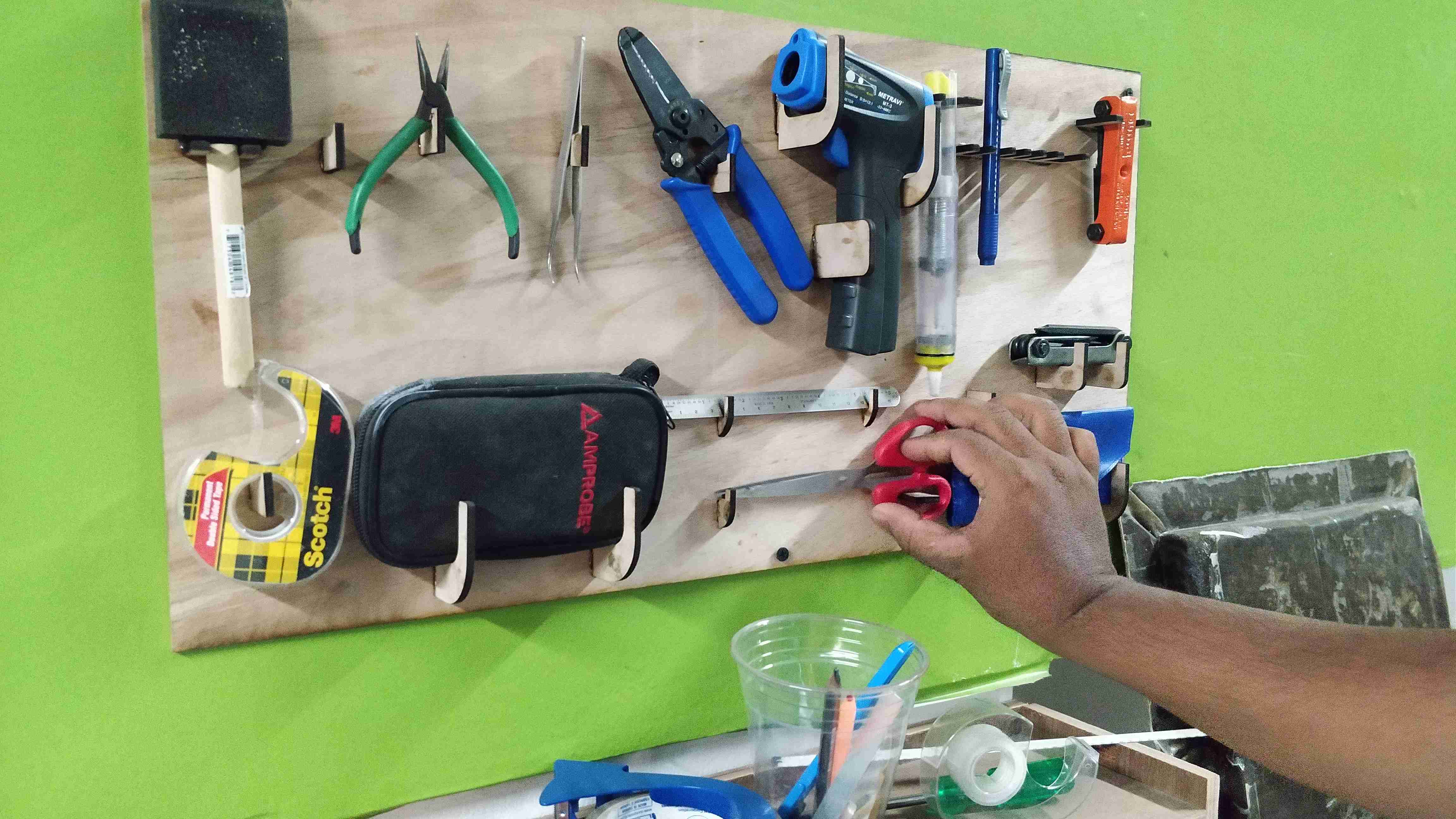
Required tools are used from the tool shelf
.
.
.
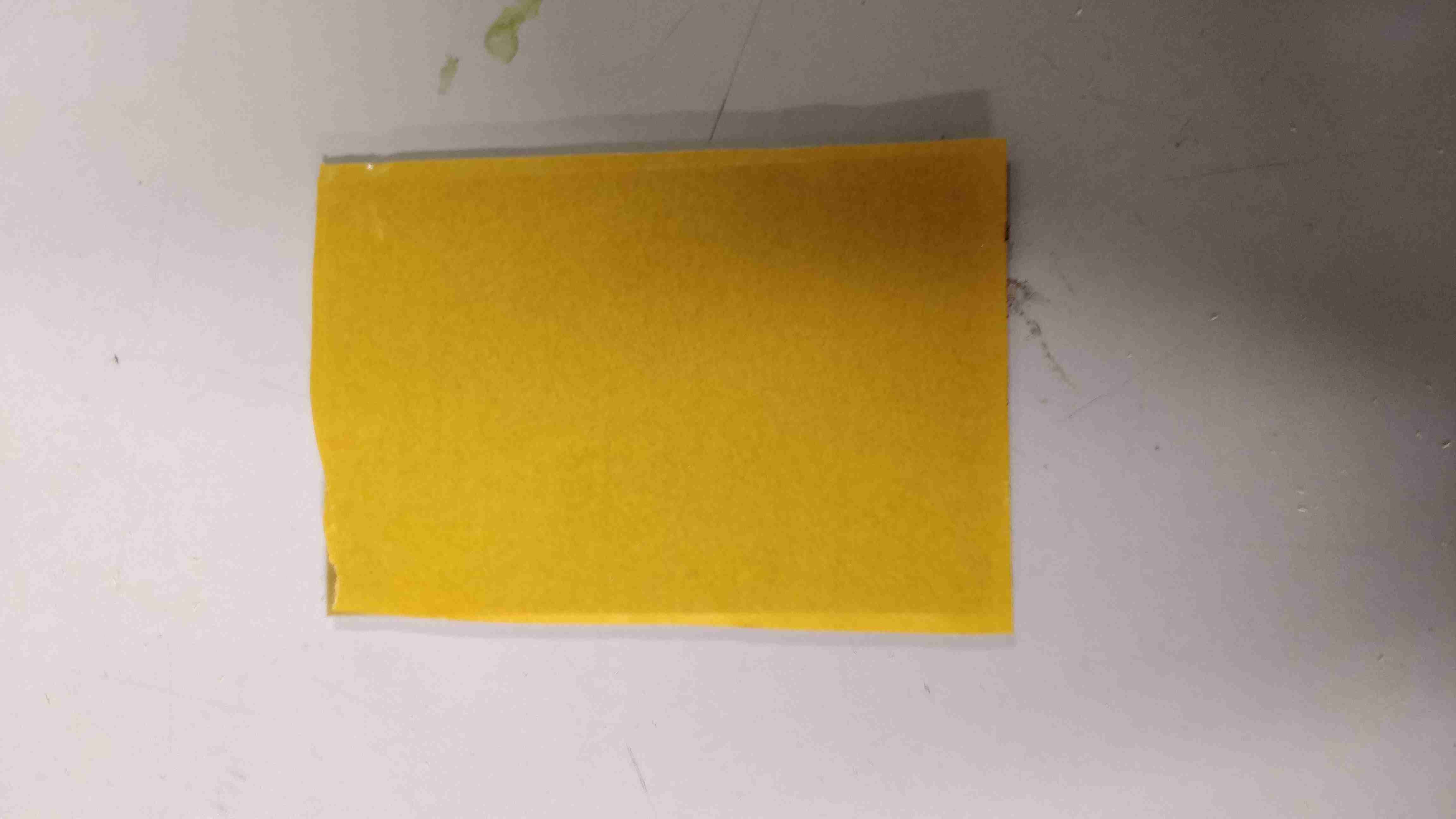
Double side tape is sticked to the FR-1 grade PCB
.
.
.
.
PCB sticked above the sacrificial layer
.
.
.
Remember to keep the used tools back in the shelf :)
.
.
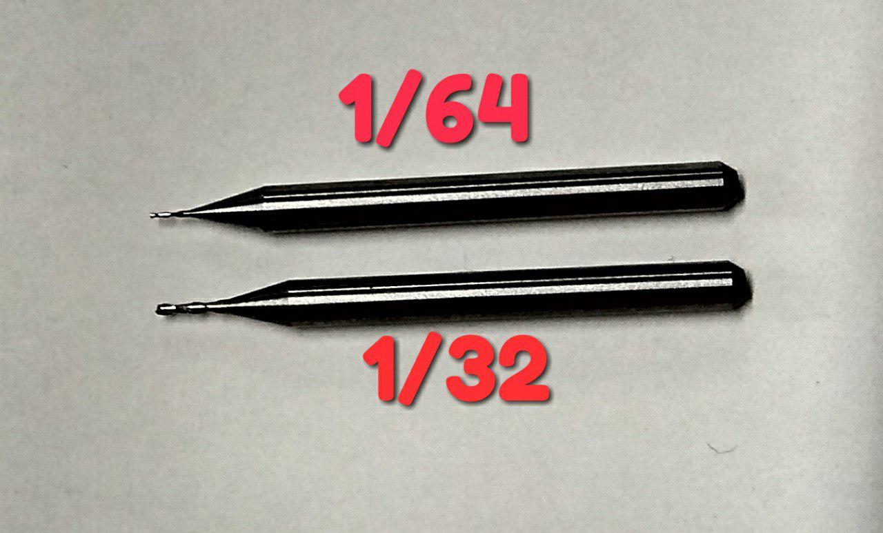
- Setting the correct bit size for tracing and milling: Two bits of size '1/64'inch and '1/32' inch is used here.''1/64' is used for tracing the PCB and '1/32' is used for cutting the border out of the PCB.
.
.
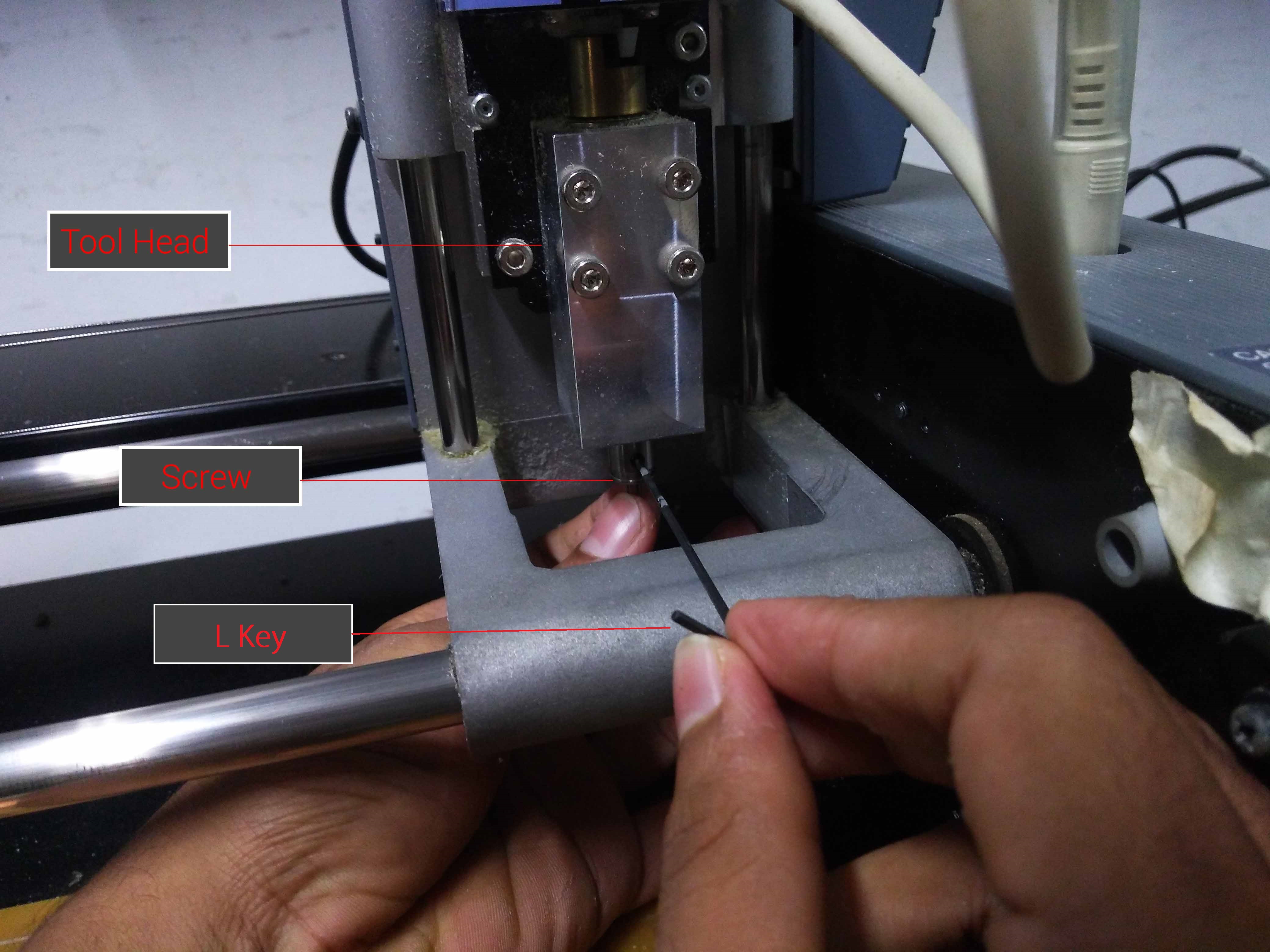
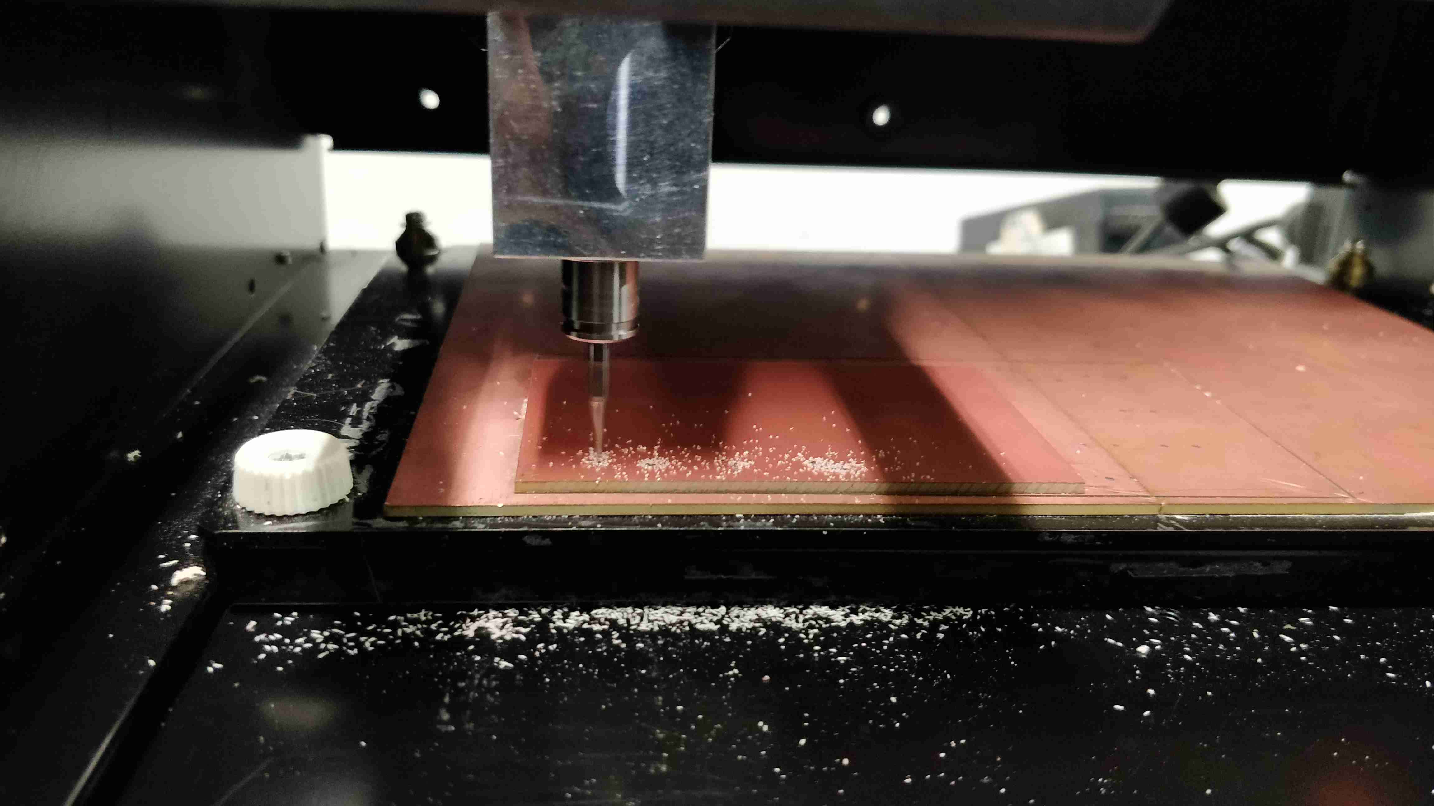
- Positioning the bit for tracing the path and Z axis: The machine should be placed in 'view' mode. '1/64'inch bit is used to trace the path of circuit in PCB. L Key is used to tighten the bit with the header.The position of bit is made higher so that it could adjusted correctly later. The View mode is retrieved by pressing the button once more. Now the machine adjusts to the origin position of (x,y,z). Now we should adjust the Z axis ie the vertical position of bit. The buttons 'UP' & 'DOWN is used to adjust the Z axis. The Z axis is thereby adjusted to a level where after that only bit adjustment is needed. Now the bit is adjusted to the height above PCB by loosening the screws with L key and then tightening at the required level
.
.
.
.
.
.
.
.
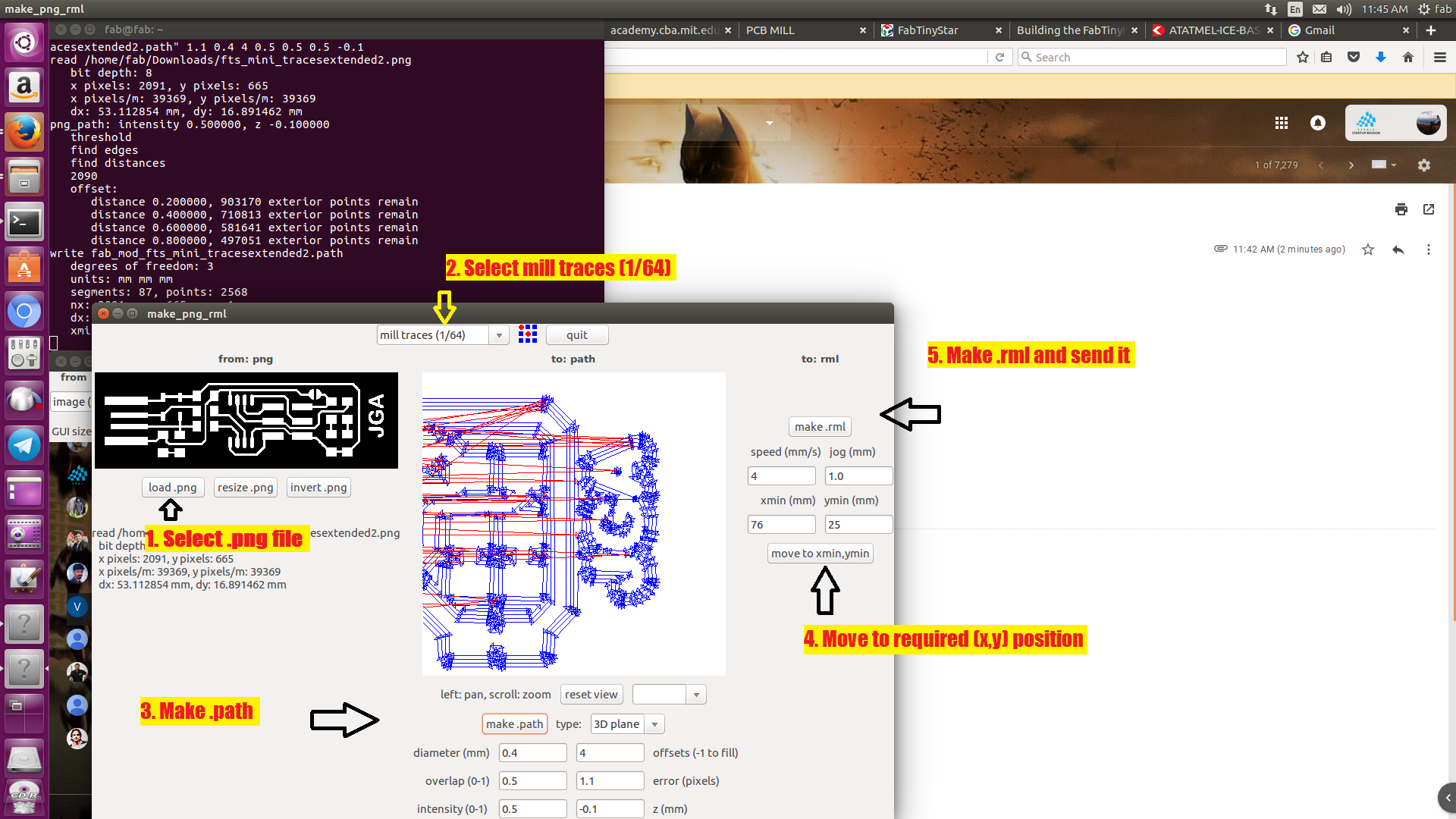
- Cutting of traces in PCB and setting up of x,y axis : Open linux terminal, open fab modules by typing fab. Follow the below procedures:
.
.
.
.
.
.
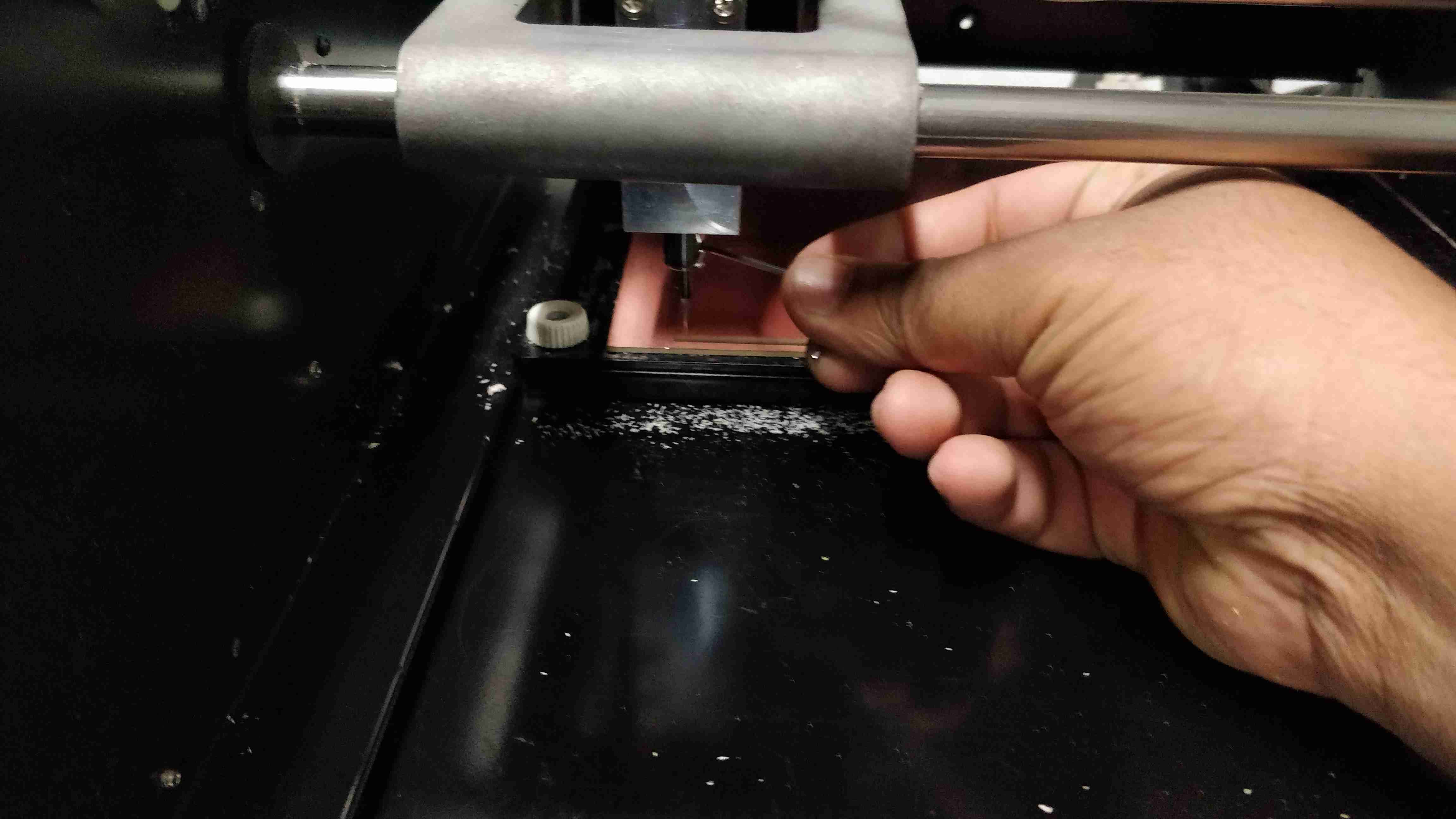
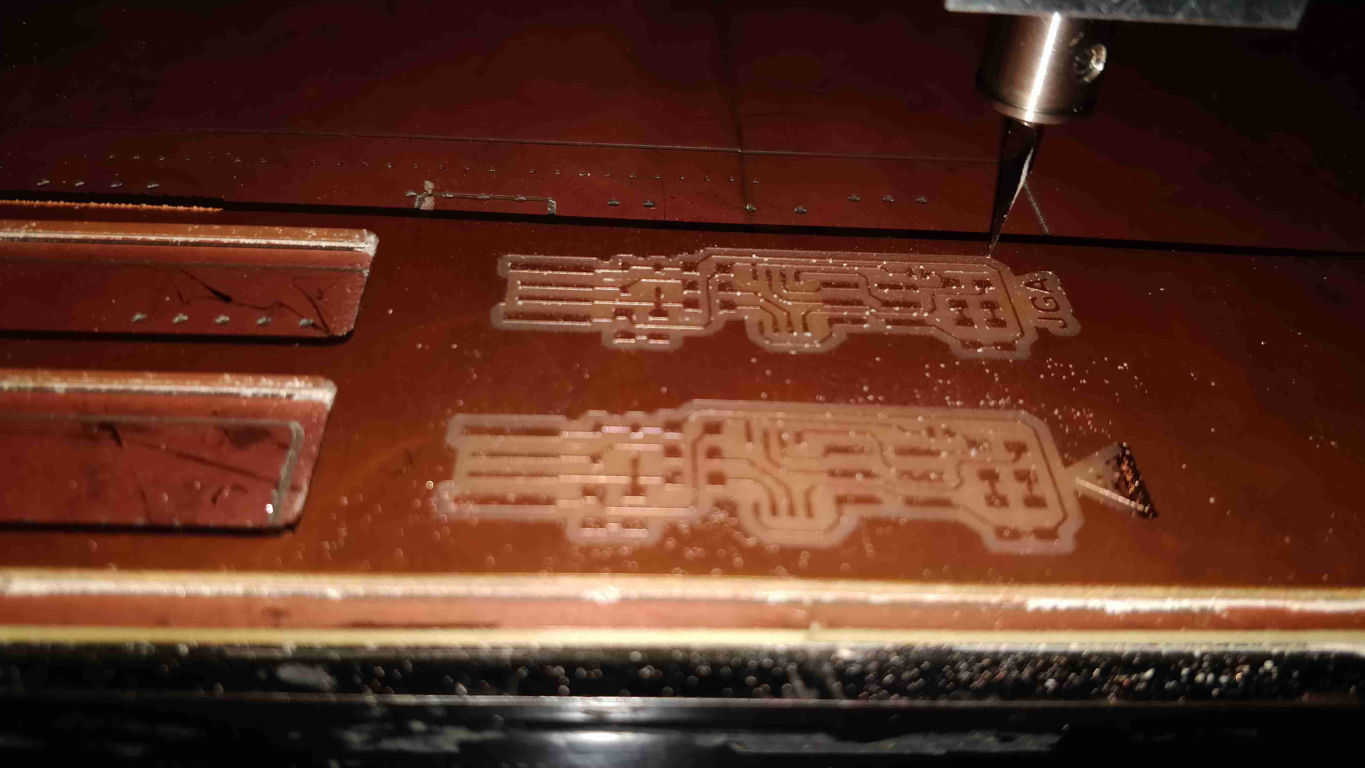
After tracing completion of PCB
.
.
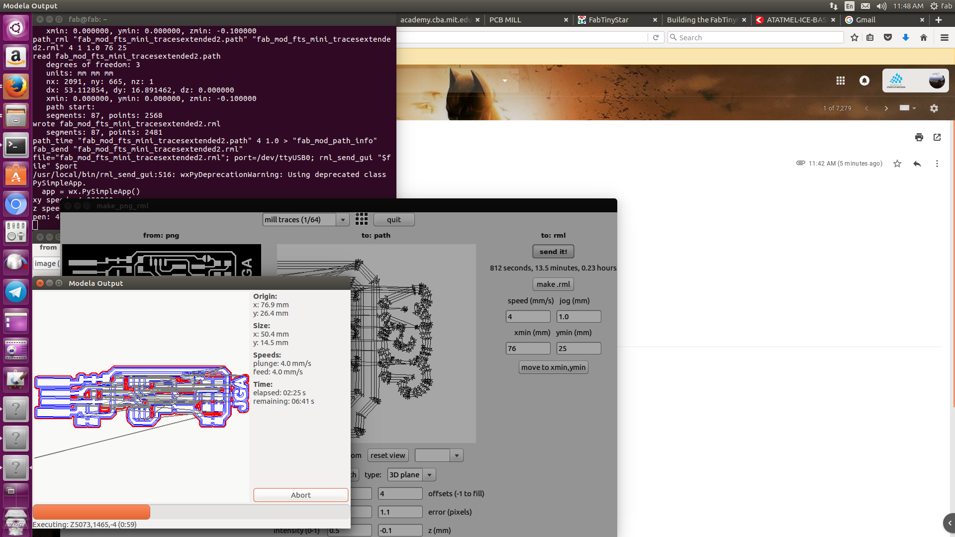
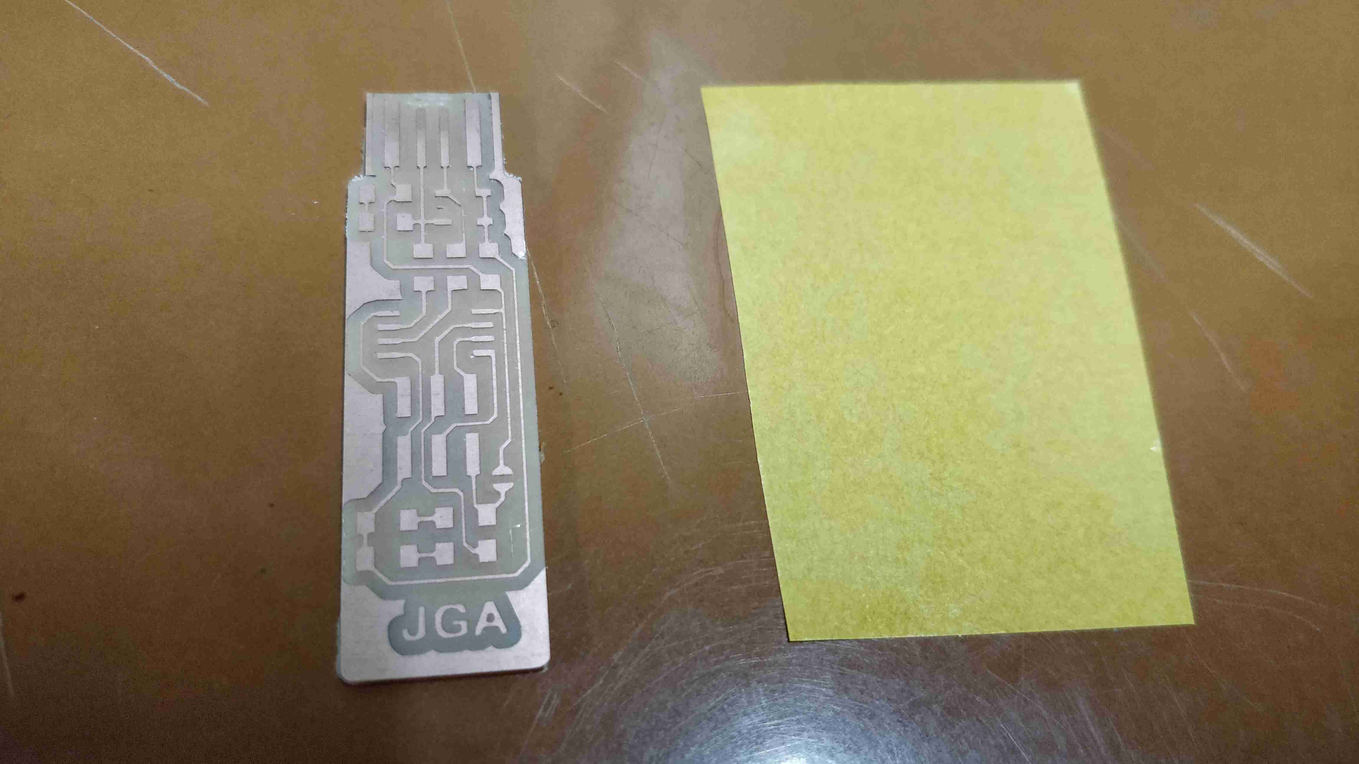
Next step is to repeat the above same steps for cutting/milling the edges of the PCB and get it removed from the mother PCB board.The bit is removed and replaced with '1/32' inch for cutting the outer edges of PCB. Then the following steps are followed: The required outer layout is loaded as png. The mode is selected as '1/32' cut board and select 'make path'.Select 'Make rml'. Move the pointer to previous pointer position by typing the (x,y) values. Click 'send it'.Now we would obtain the PCB removed from it's mother PCB board
.
.
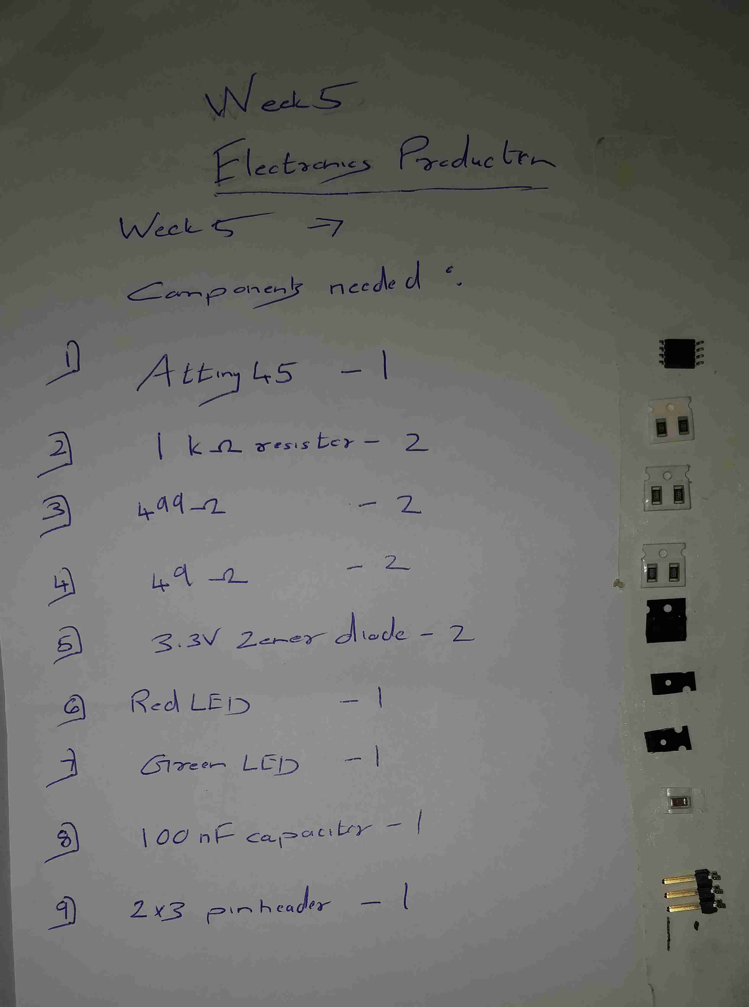
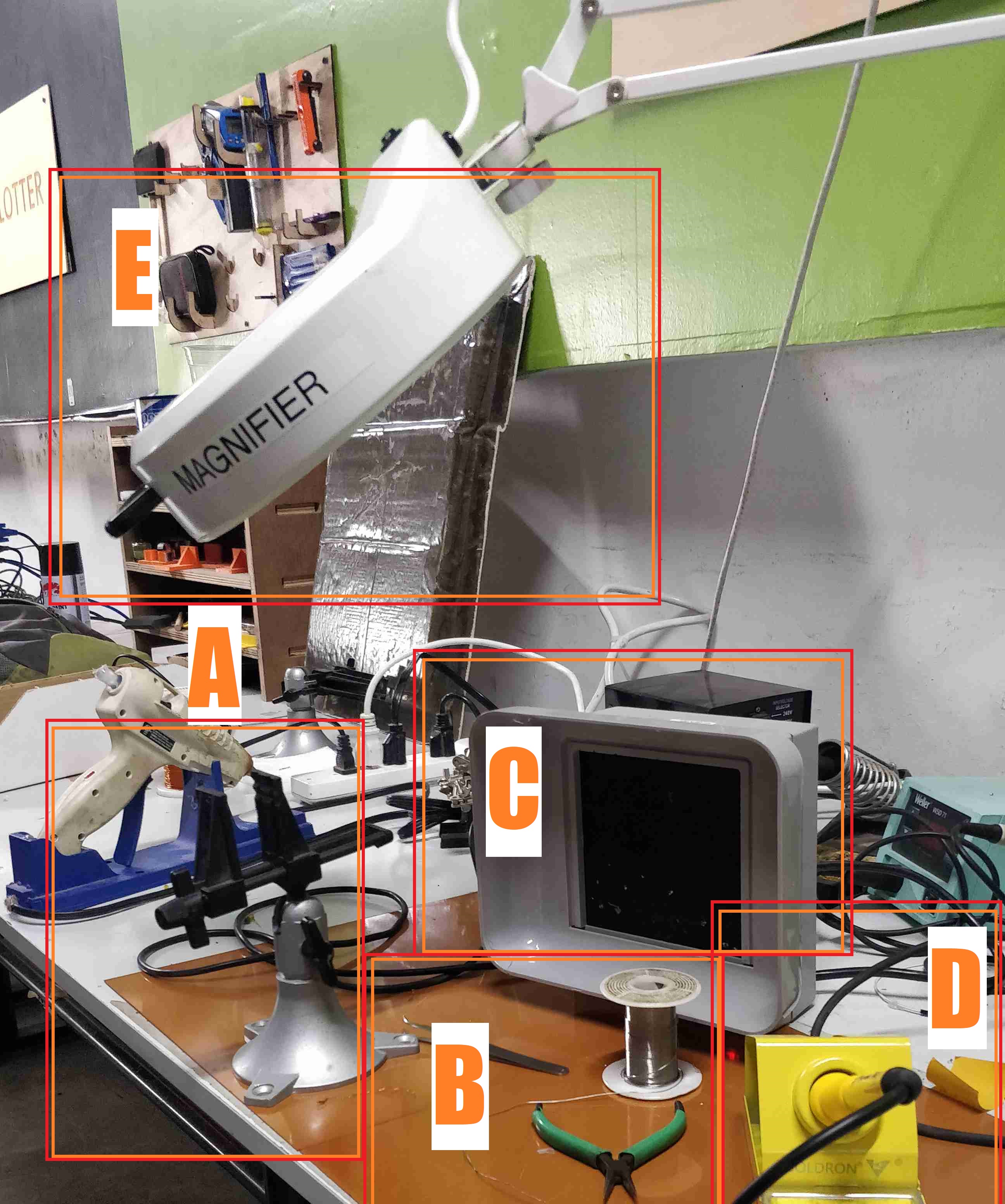
- Obtaining the components and soldering them into PCB : First step is to have study the component diagram an d make alist of the components required for soldering the board.The list is then created and required items are pasted into the sheet using a double sided tape as below
.
.
.
Make a list of components and pick and place each component from store to paper
.
.
.
Make ready the soldering station for soldering the components to PCB
.
.
- A. Helping hand
- B. Soldering wire,Tweezer,Nose Plier
- C. Fume extractor
- D. Soldering iron
- E. Magnifier
The soldering iron was set to 280 celsius , the components were soldered one by one with the help of the above equipments.Multimeter was used to check continuity of the circuits during each steps.Also it was used to check whether the diodes were forward/reverse biased.
.
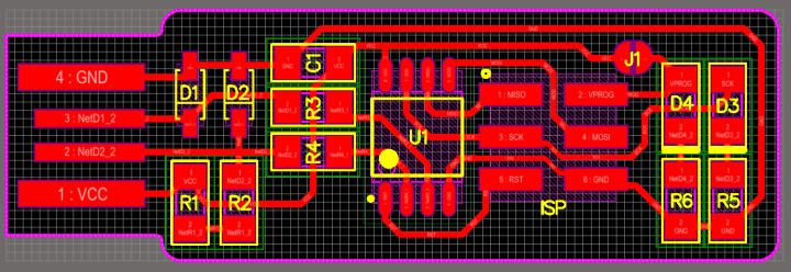
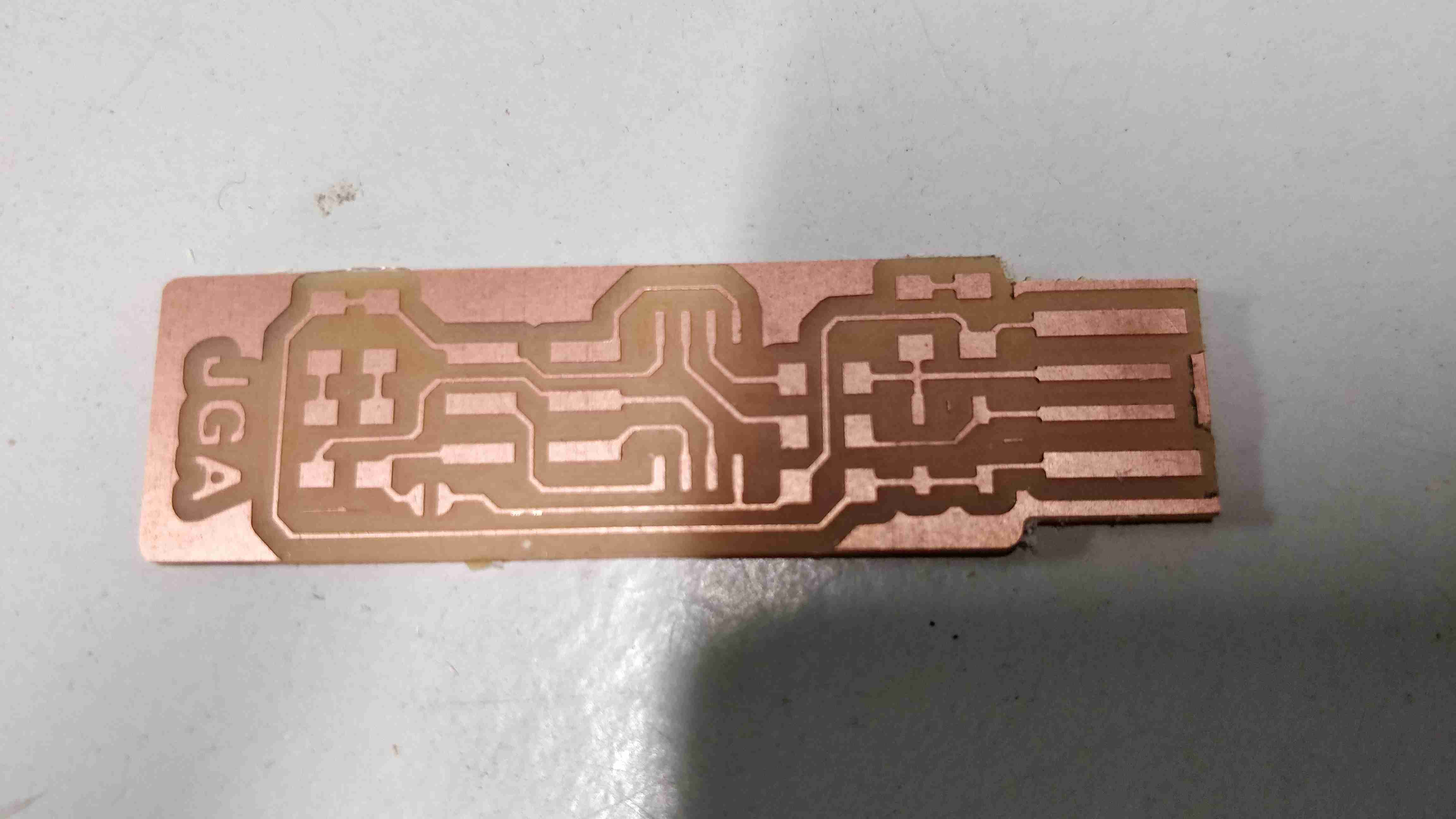
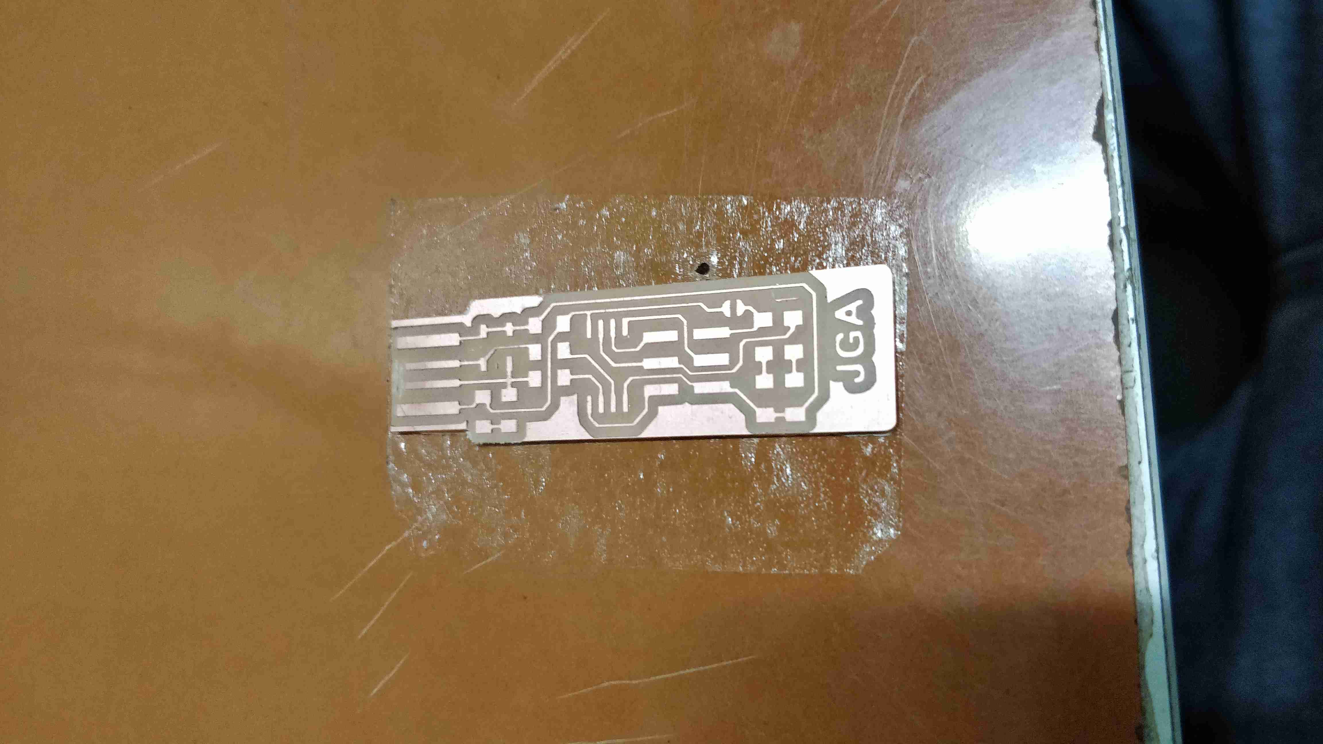
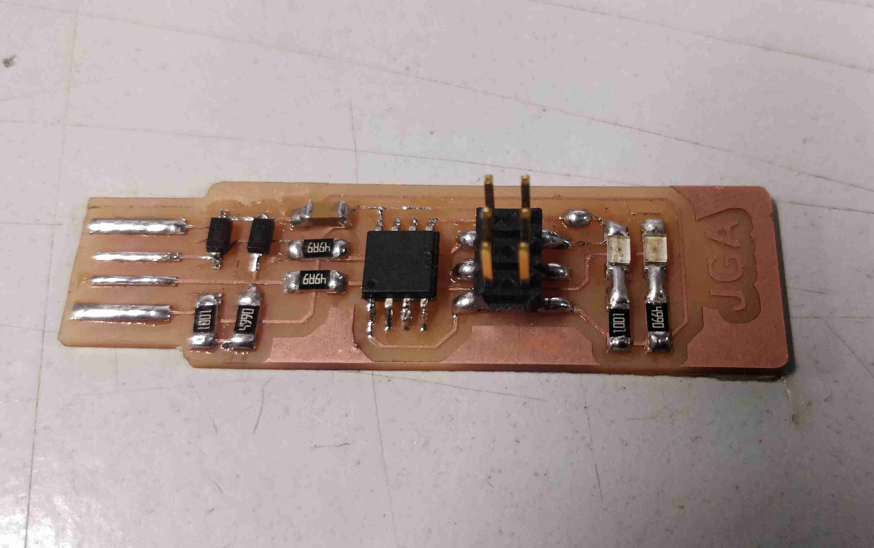
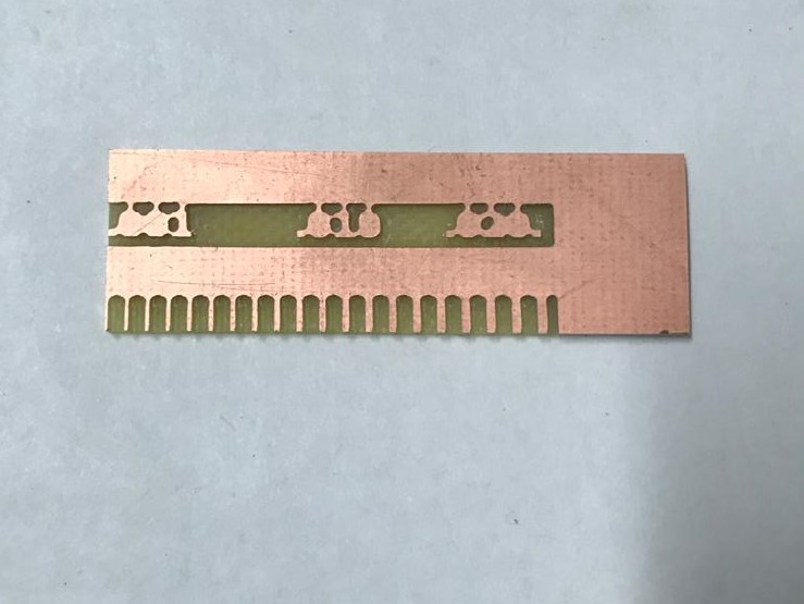
Finished PCB board
.
- Programming the soldered PCB- FabTinyISP : Before this we should look for any loose connections, misalignment, orientation of components and make the board have a finishing touch.
Software installation and Building Firmware
- For installing avrdude, open a linux terminal and type sudo apt-get install avrdude gcc-avr avr-libc make
- Download the firmware source code from here . Extract the file to a specified folder lets name it 'fabisp'
- Open linux terminal and move to the 'fabisp' folder created earlier using the change directory 'cd' command
- After entering the directory , inorder to make the required .hex files for flashing into the microcontroller. Type make. It will make a corresponding .hex file ie, 'fts_firmware.hex' in the same directory
- Next step is to program your microcontroller by flashing this .hex file. The makefile which is in the folder is the file which gives directives and tasks to be executed. We need to edit this make file using text editor and change certain parameters as required. Such as the makefile will have the following text:
PROGRAMMER ?= usbtiny
We need to change 'usbtiny' to whatever programmer you're using, if only we use another programmer
.
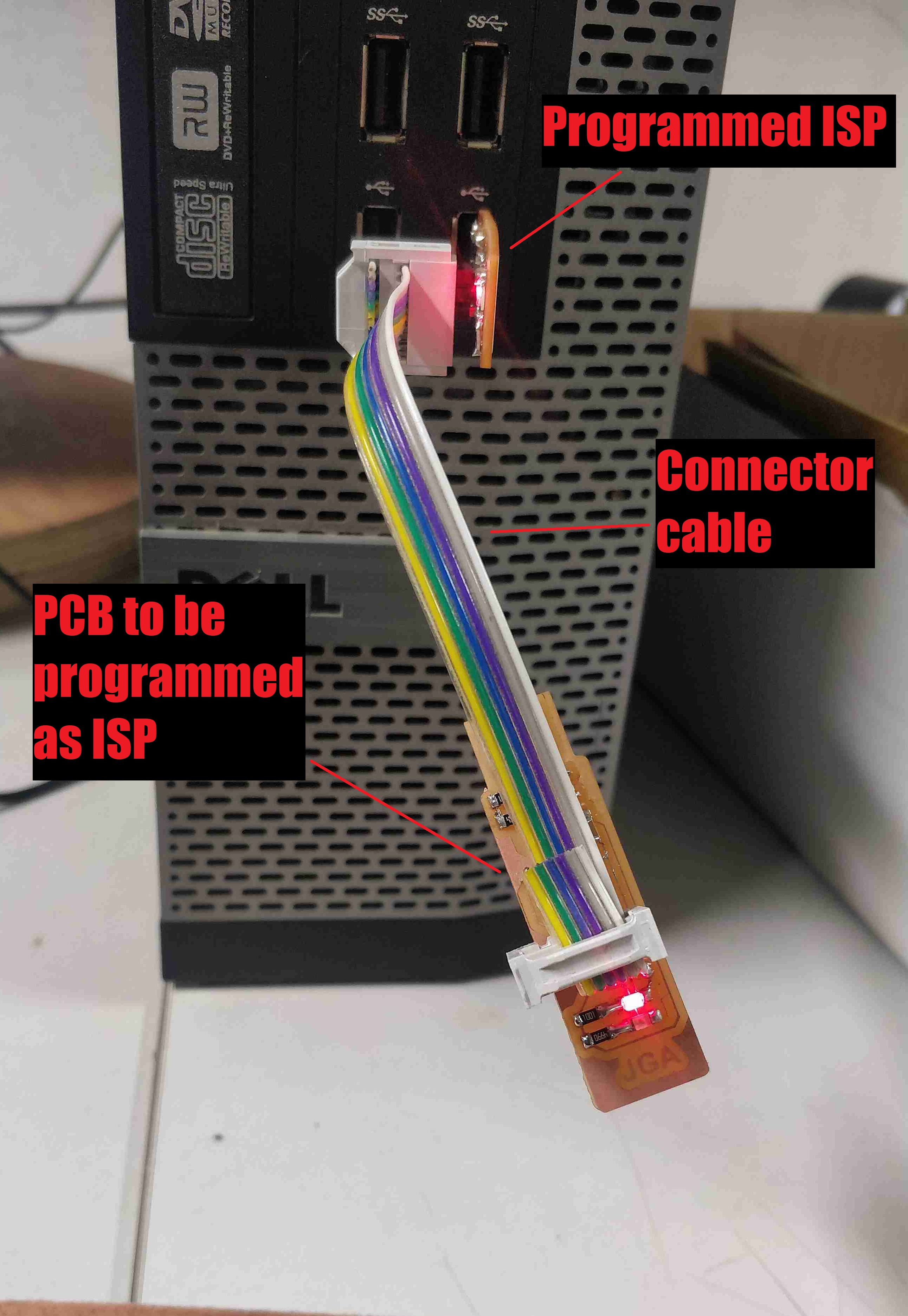
- After the required changes in makefile the PCB ISP header is connected to another already programmed ISP programmer as shown here. Since our PCB wouldn't be knowing how to communicate with USB port , another ISP is required to program it to the requirements. The ISP headers in both PCB's are connected such that same pins are connected ( ie MOSI to MOSI, MISO TO MISO etc) .
- The USB pin of the already programmed ISP is connected to the USB port of the system where the linux terminal is running.Since red LED is connected on VCC red lights on both PCBS will be turned ON
.
.
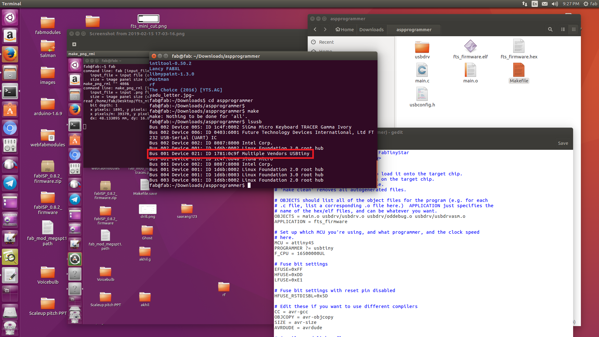
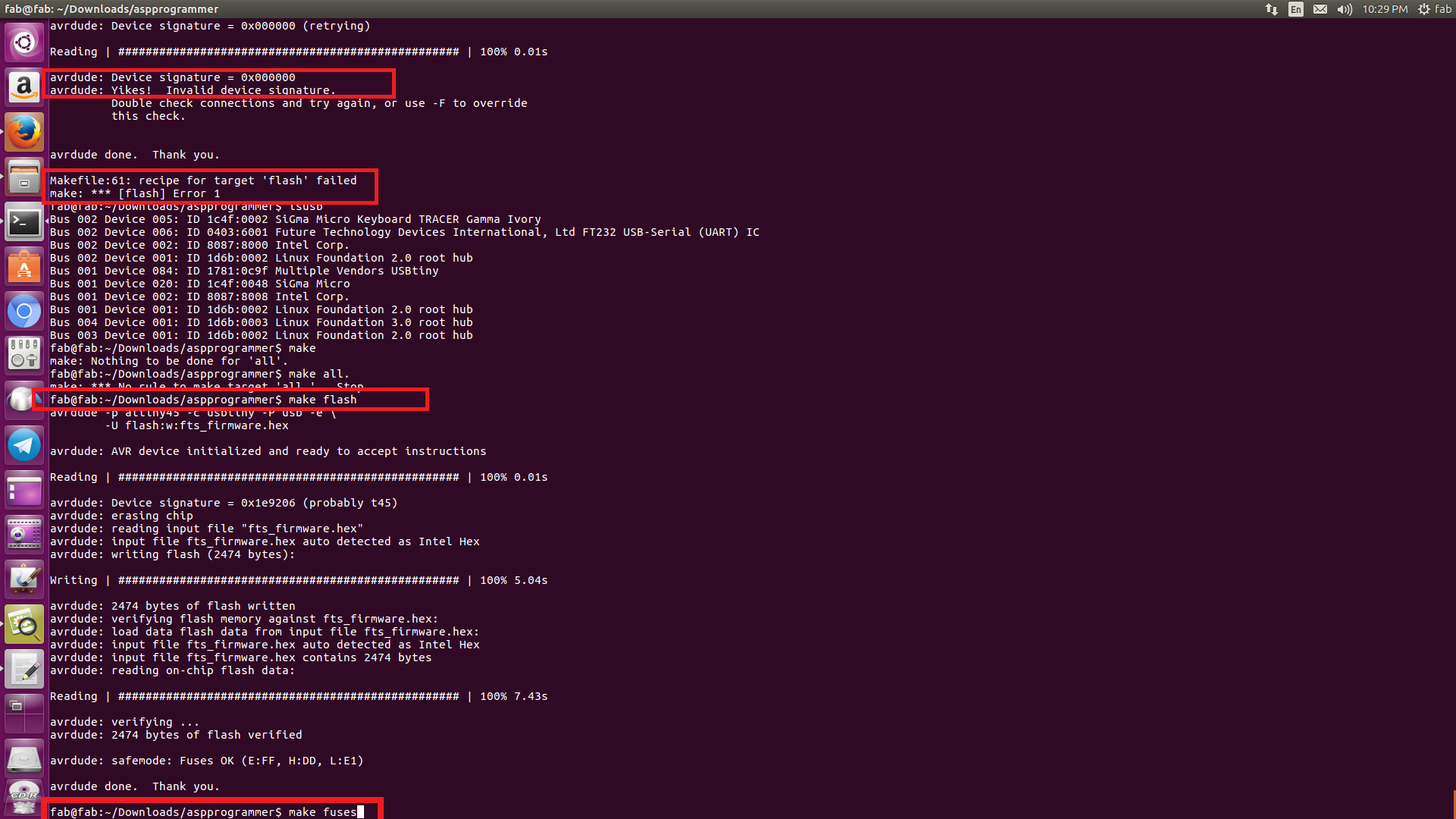
- To check whether the usb is detected Type lsusb in the linux terminal. Check whether the system detects any usbtiny devices as below:
.
.
- Since the system detects the device, next step is to flash the .hex file which was made earlier.Type make flash on terminal which will flash the hex file to our PCB
.
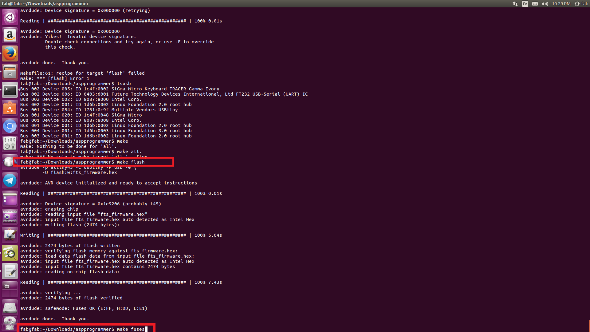
.
After the successful flashing of the file, we need to set the fuses. Type in terminal make fuses. This will set the fuses except the one that disables the reset pin
NOTE : Understanding fuses
Every AVR microcontroller, from the ATtiny in your thermostat to the ATMega in your Arduino, stores its configuration in a series of fuse bits. These fuse bits control settings such as the multiplier of the internal oscillator (and thus the speed of the chip), or if the reset pin can be used as a GPIO pin.
To understand more click HERE
Also there is an online fuse calculator for getting the fuse values HERE
.
- Next step is to disable the reset pin and use it as I/O pin and disable reprogramming of the microcontroller in future. Connections should be made as previous ie, USB port to ISP programmer to our PCB. Type rstdisbl in terminal. Now the RST port is disabled
.
- The issue i had faced with this is that when i flashed it for the first time in my linux system, 'Device signature error was shown'. Later i connected it to my friend's windows PC and flashed it using GIT bash. This time it was successfully flashed. Then i returned it to my linux PC and flashed it again, but this time it was a success. I don't understand why the error came up on the first time.
.
.
Group Assignment
.
The group assignment was to find the mill resolution of the bits ie '1/32' inch and '1/64' inch bit
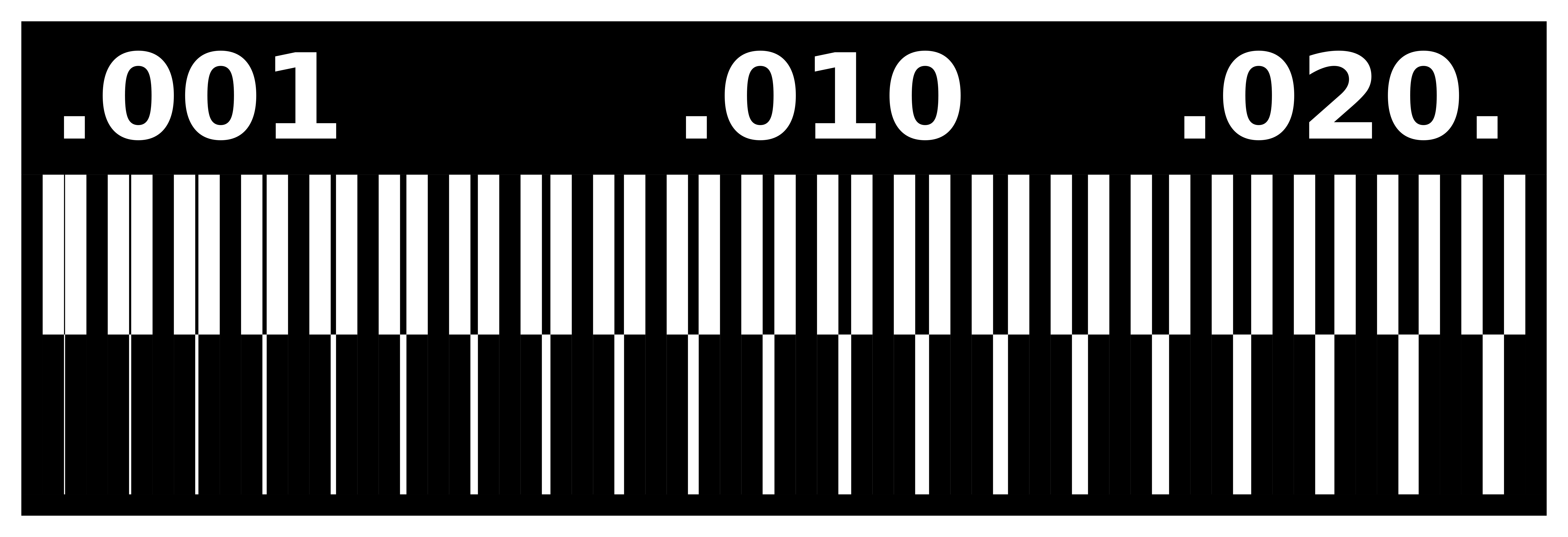
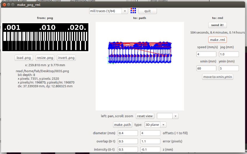
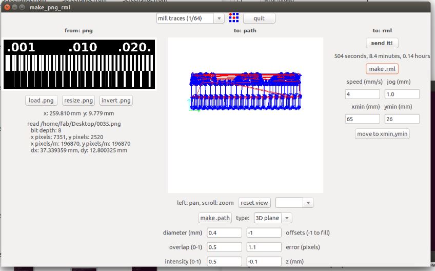
First we use '1/64' bit with 4 as offset and load it in fab modules as below:
.
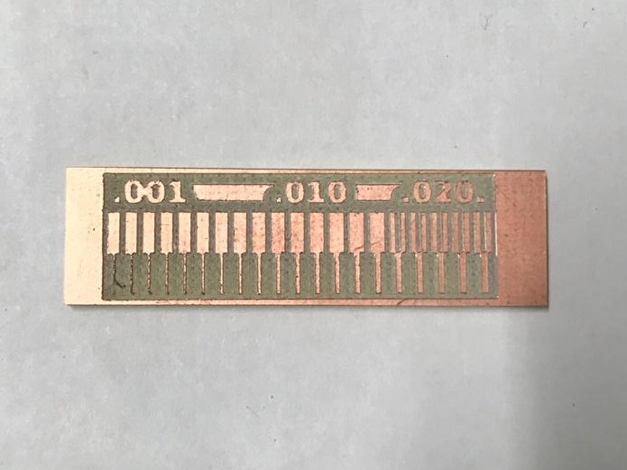
.png file for milling varying from .001 to .02
 Download file
.
.
.
For this configuration ie '1/64' with 4 as offset you can see parts of copper are remaining in the PCB. Next we should try '1/64' with -1 offset
.
.
.
.
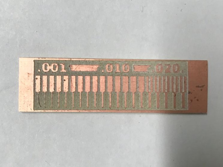
In this configuration '1/64' with '-1 fill' ,the milling is fine
.
Next step is to use '1/32 inch' bit for milling at -1 offset
We could see the output as below
.
.
.
From this output we can conclude that '1/64' bit with -1 offset is suitable for milling and '1/32' cannot be used for milling but to cut the PCB