Week no.6
- Electronics Design
- PCB Schematics and Layout
Assigments :
- Redraw the echo hello-world board
- Add a function like a button and LED
- Check the design rules, make it, and test it
Re-Designing the Hello Board
Preparation
I´m an old user of Eagle Schematics, started to work with it at more than 10 years ago, at that time it was still developed by CadSoft Company. But I hadn’t made any schematics for the last 5 years, so I was afraid it may be very different from the eagle I used to know (Used until V4.1 I think).
So I used my Autodesk Account to download and install the new eagle 8, what I realized is that didn’t had changed much (besides installation and oppening page). The procedure of adding libraries was the same, so I downloaded and placed into Eagle LBR folder the SparkFun Eagle Library and the components Library for FabAcademy.
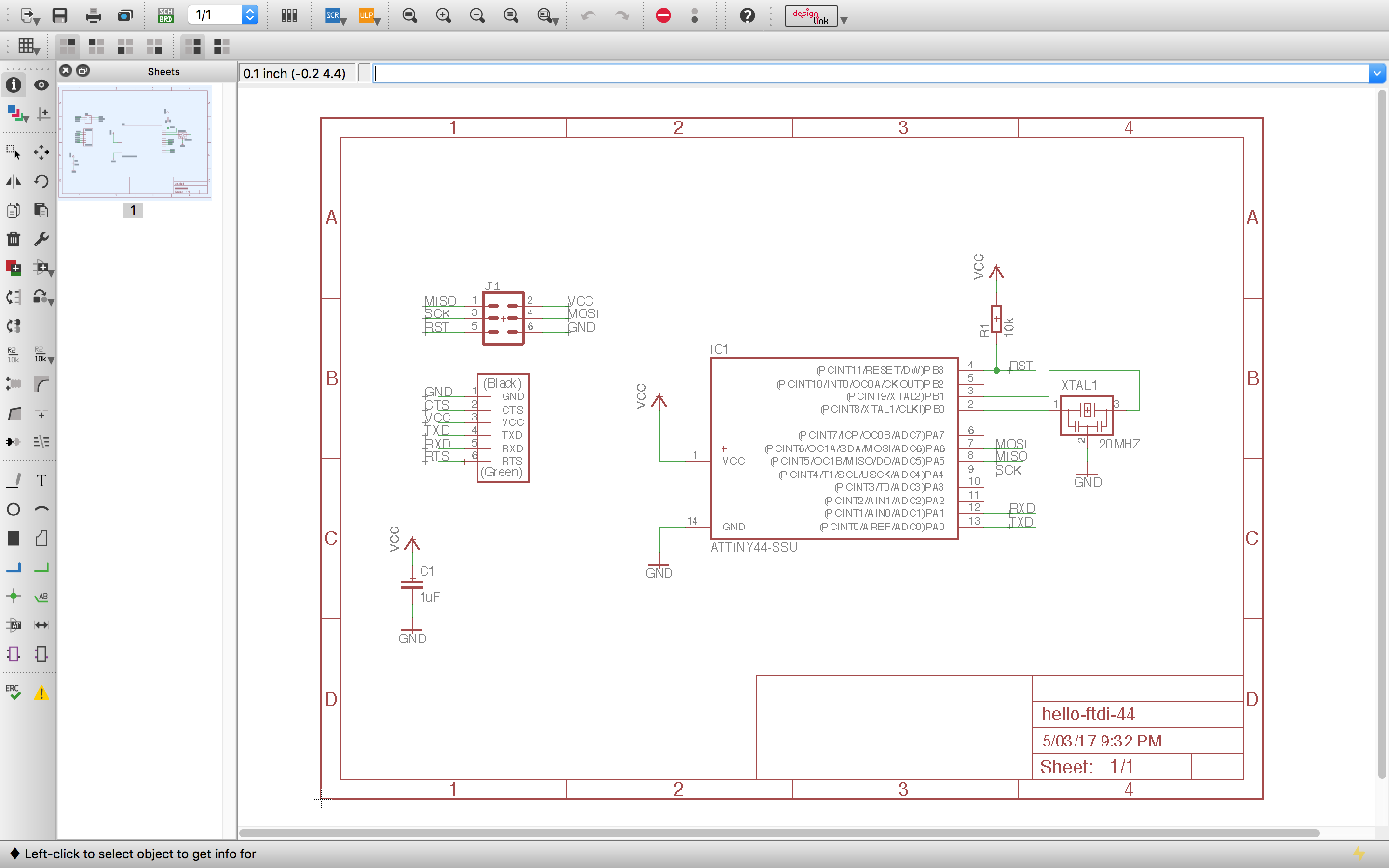
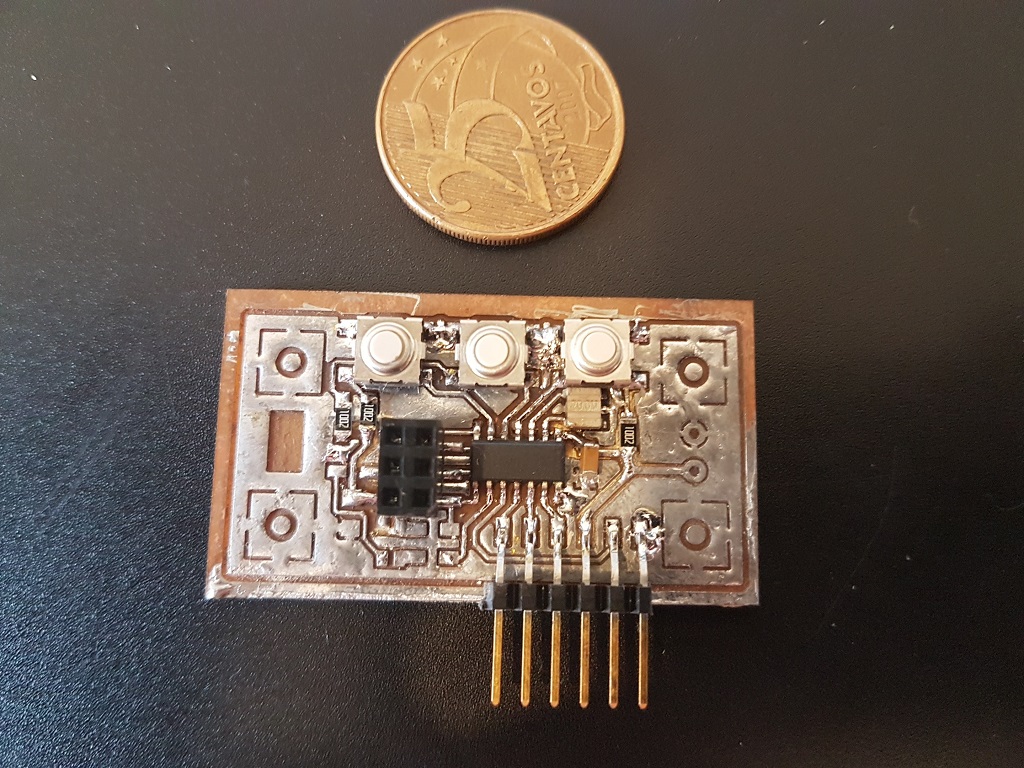
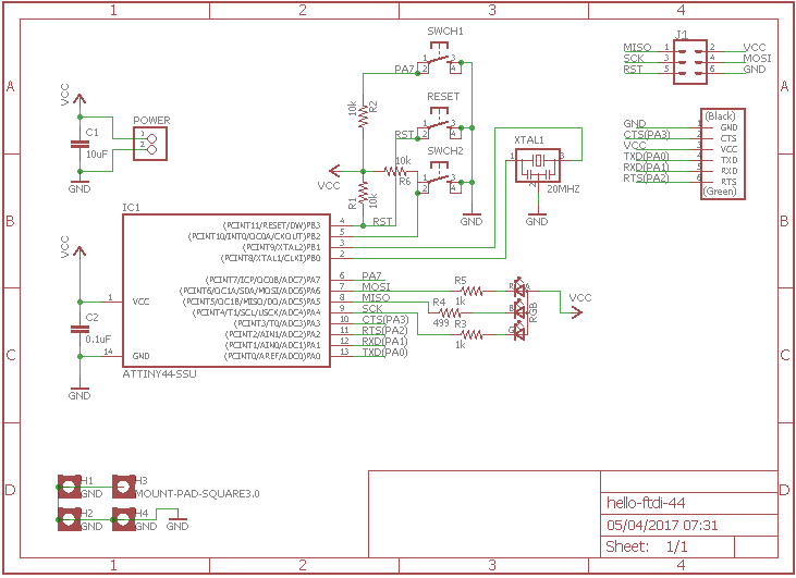
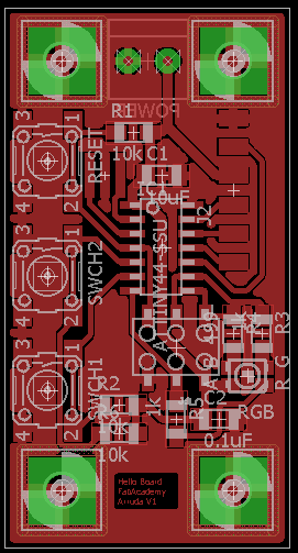
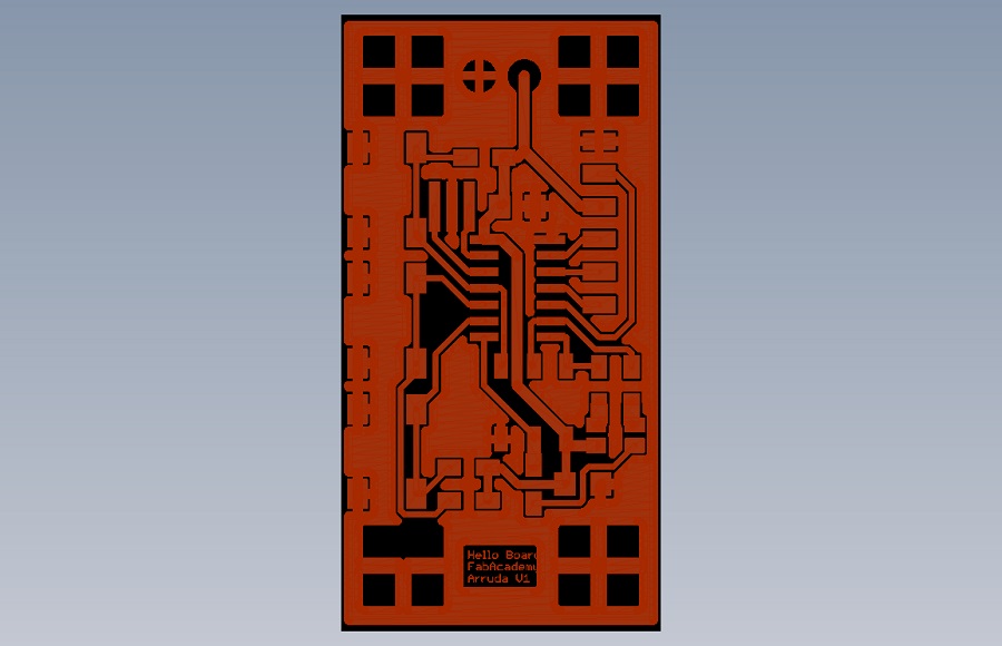
Create a FabAcademy Project Folder and Started with Eagle and the sample Hello Board schematics, the idea was to make a flexible (all unused PINs out to a connector) board adding elements that should be of interest to further assignments and final project like test Buttons, Leds, sensors and Display.
And so were added some (usefull) components:
- 3 Buttons - to test interface and user navigation
- A power Connector - 2pins (VCC+, GND)
- 2 capacitors - 10uF at processor power pin and other 0.1uF near the ISP connector
- A RGB Led - Status and debugging
- Upgrade to FDTI connector - Pushed out unused pins
- 4 Mounting Holes - Grounded pad for screws
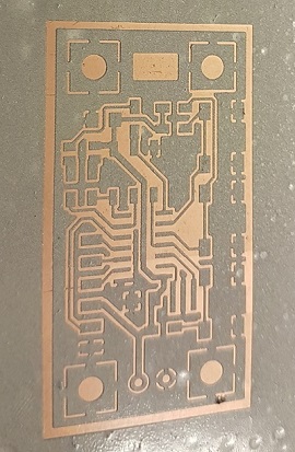
Routing the Board
Actually were made 3 versions until reach the final design. Considering the small size and few components, it was an obvious choice to route all components manually (None Auto-router). The design rules for the Hello Board meet the following requirements:
- Clean and small design, single sided
- No jumpers or wire routes outside the board
- Filter capacitors near the microprocessor and another near the SPI VCC
- Take benefit form remaining un-machined cooper surface for ground shielding and improved stability
- All processors pins accessible through a pin header
- Could be screw mounted to a case ..
- .. or become an user interface along with a Display using the SPI or FDTI connector
- Respect tolerances, outlines and isolation, approved by Eagle ERC/DRC check !
Routing Hints :
- Double check signal names used like VCC or GND, careful not to add a second source power like VCC+ doing so you will have separated signals.
- Create a polygon around your board and name it GND (or the ground signal you used), it will create a mesh of ground around your wiring. This is good, for the mill bits, for the electromagnetic shielding, for a stable GND, for testing after with a multimeter, all gain. But you need to remember clicking Hatsnest.
- Put names and annotations on wiring at Schematics, is nice to remember and check signals afterwards.
- Check your connections with the SHOW tool (the eye) if you open both Board and Schematics on screen it will highlight your signal in both windows.
- Do a ERC check and SHOW ERRORS, check the clearances, it will ensure you get no shorts when soldering !
PCB Fabrication - first attempt !
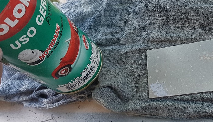
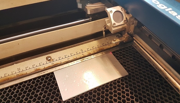
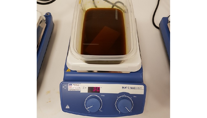
I tried to use a new (actually an old) fabrication method to produce the board by chemical reaction with iron perchloride. But to draw the schematics layer on the board I used the laser-cut machine. Our laser-cut is not full spectrum and has low power (40W), and so it has power to only vaporize a thin layer of a protective ink previously applied. It works beautifully, incredible precision and finishing!
This fabrication method can be archived by following these steps:
- Prepare the PCB to the desired size
- Create and save file of circuit board traces (PNG)
- Apply a thin spray ink layer to protect the cooper
- Engrave the traces file with the laser-cut machine to the PCB
- Prepare the iron perchloride solution and submerge the PCB
- Stir the solution, if available, provide heat to accelerate the chemical reaction
- Clean the PCB board and you are done !
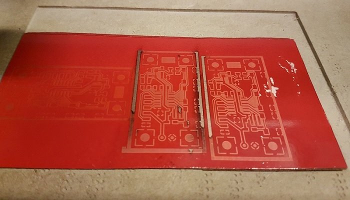
FAIL : Choose carefully your ink ! The corrosion didn´t worked as expected, the laser cut couldn´t remove the ink leaving a very thin layer. It was probably because I used a automotive spray with metal particles. The last picture above shows a second try with red spray ink with the same effect: I tested different speeds and power for the laser, at some point the laser burned the metal layer finally exposing the cooper. I suggest look for the ink composition and choosing a non metal based for this to work !!
And here is a video of the laser "etching" for the Hello Board:
PCB Fabrication - second attempt !
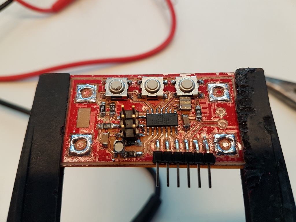
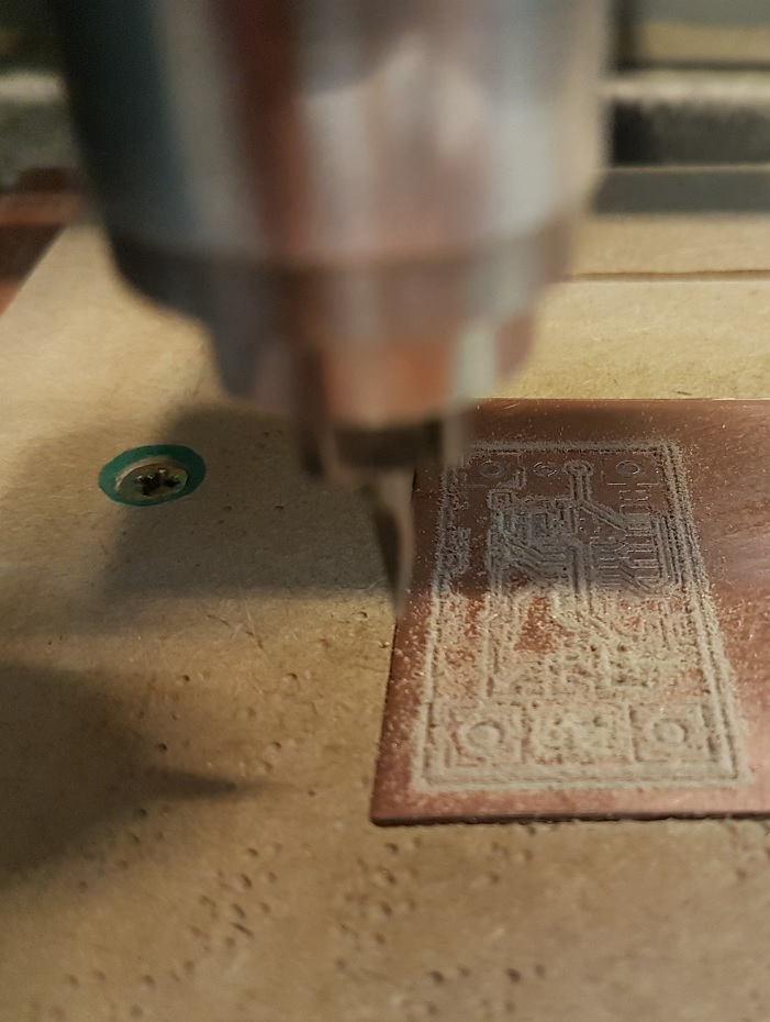
Ok, after the failure I went back to the milling process! But I reused the laser test board (painted red) to take advantage of the isolation ink layer (let´s try it). So by the pictures you can see a cool red finishing in the milled board, of course I needed to scrap the ink prior soldering. Also made another one (Silver) as a backup in case I couldn’t use the painted version.
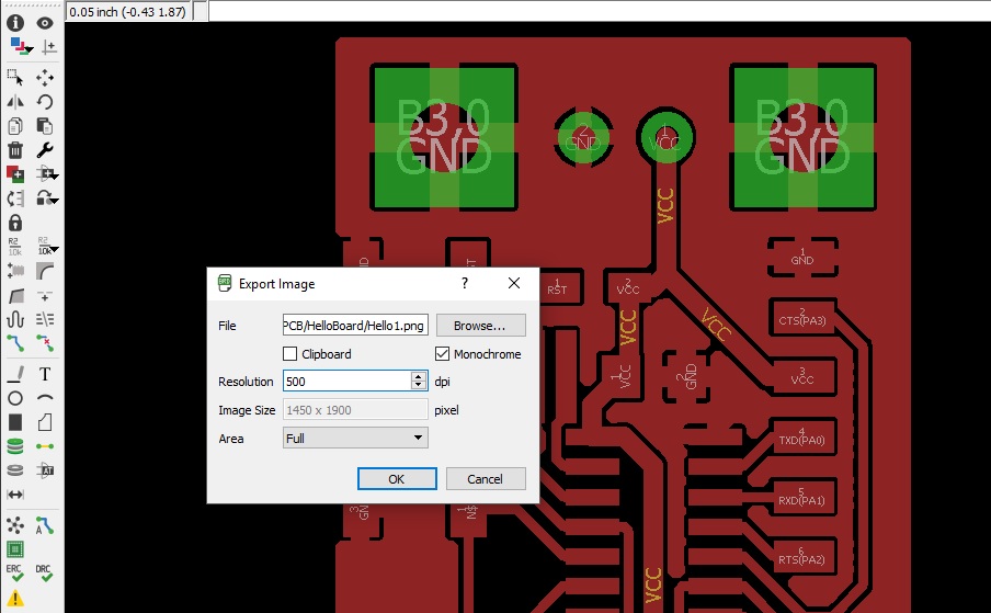
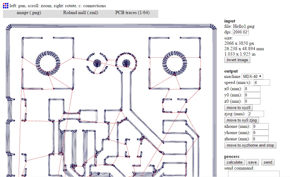
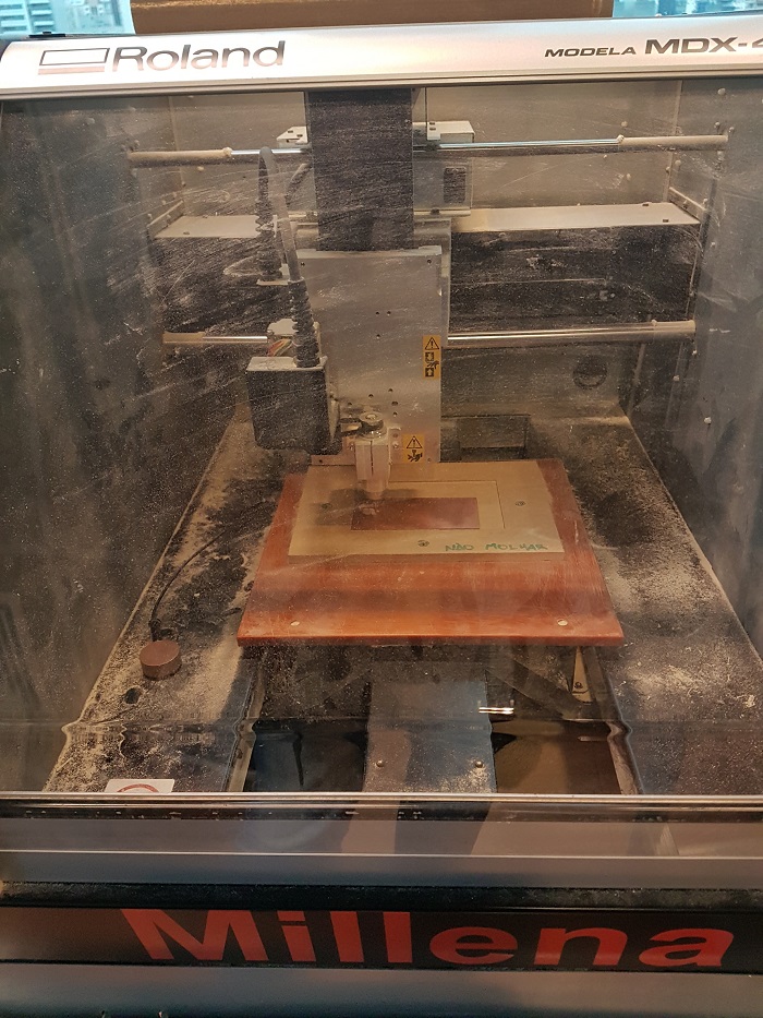
Exported the TOP Layer and the OUTLINE to PNG files and used the Fabmodules procedure (Week4) to generate the G-CODE. Opened in Roland VPanel, glued the board with double side tape, referenced the mill bit at the Board surface and executed the machining. Swipe the pictures below :
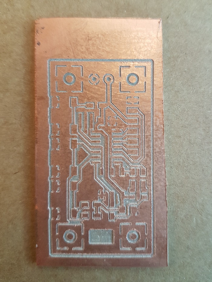
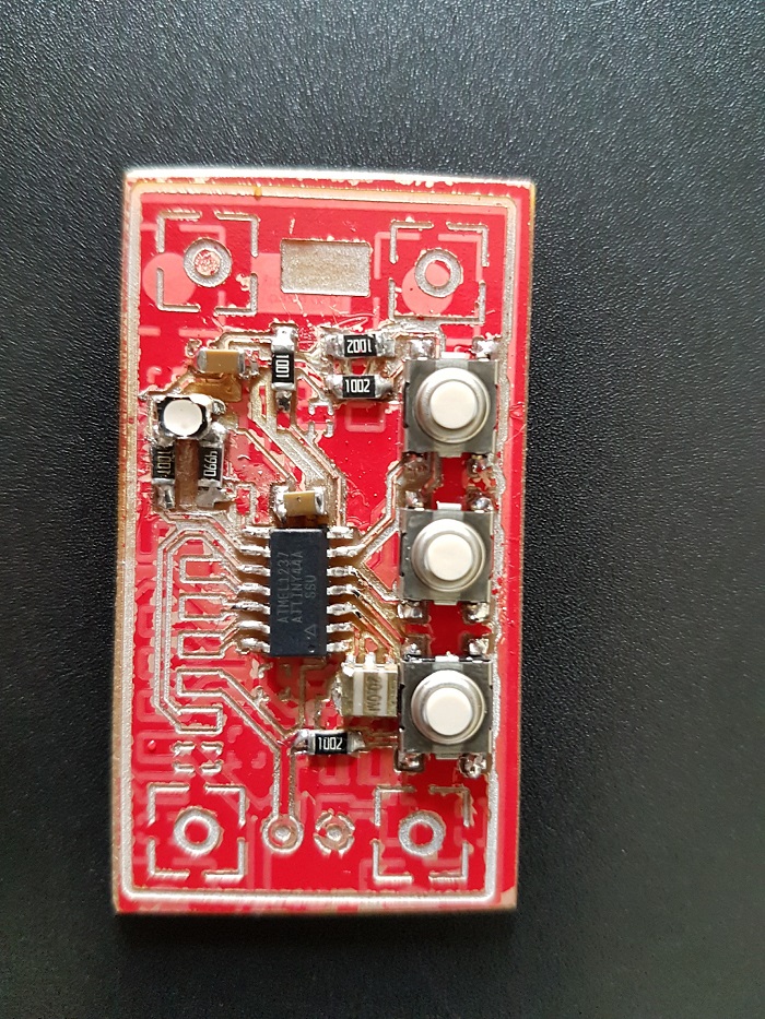
Ok, I agree the RED has not a good appearance but it works. The SILVER version had a better finishing as you can check in the pictures: