Final Project
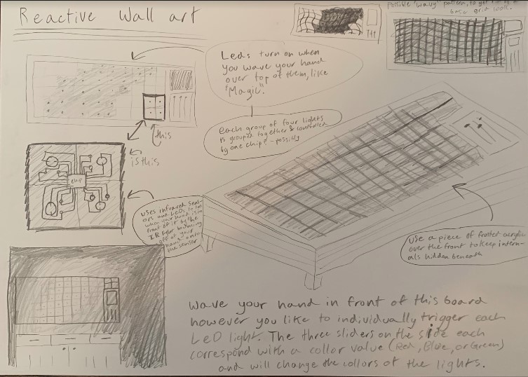
For my final project, I initially wanted to make a large wall display that would be sort of like an interactive art installation. After more planning and learning over the course of Fabacademy, though, I am coming to realize that I might have been too ambitious with my idea at first. I wanted to make a large wall display with many different LED lights in a grid array that would turn on when you waved your hand over them. I would have put it up in my schools art/engineering hallway for other students to use and enjoy, and the main goal really was to create a project that effectively blended art and aesthetics with technology and engineering.
The issue with my first goal was really just the cost. The components for such a large project with so many individual intricate systems for every single light would have ended up totaling well over five hundred dollars USD, so I figured I should consider pulling it back a bit.
Now, rather than making a single huge piece for my final project, I want to make a smaller example that shows the functionality of the project in a more compact, 4x4 array of LEDs.
Initial Planning and Research
Research
My plans for this project all started when I bought a sauter kit on adafruit called Octolively. The kit operates based off of the effect that Infrared LEDs have on Infrared Photodiodes. When light from one of the IR LEDs is reflected off of your hand and back into the Infrared photodiode, that photodiode reacts in a way that can turn on another, larger LED that is intended specifically for lighting. The kit itself is quite small, but when you chain a bunch of them together, as seen here, it has great potential to be a really beautiful and aesthetically pleasing piece of digital artwork.
Another thing I want to consider when planning and working towards this is how I could actually give the LEDs a fade effect. I think that if I can use a specifically valued capacitor in line with the LED, the residual current in the capacitor could power the LED for a bit longer even after your hand moves out of the way and stops reflecting the IR light.
After coming back to the idea towards the end of Fabacademy, I’m starting to see how my revised final project idea is pretty similar to the initial solder kit that gave me my inspiration. To be clear, my goal isn’t just to make a small, fun kit that’s exactly the same as the solder kit. I want to make a small proof of concept for a larger installation that would be my own creation.
2D and 3D Modeling
As of right now, I’ve only sketched out a few ideas, but I intend to create a 3D model of the piece eventually.
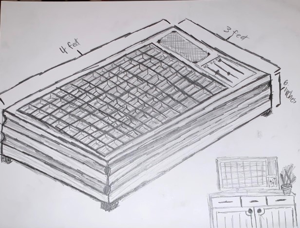
At this point, I have created a model of the revised project in Fusion 360. All it shows is the control box that would go in front of the viewer, not the light panel that would be on the wall in front of them.
Materials
| Qty | Description | Price | Link | Notes |
|---|---|---|---|---|
| 1 | Op Amp-TLV2462 | $2.95 | https://www.adafruit.com/product/808 | Order Two |
| 1 | IR LED and photodiodes | $5.28 | https://www.amazon.com/Gikfun-Infrared-Emitter-Receiver-Arduino/dp/B01HGIQ8NG/ref=sr_1_1?ie=UTF8&qid=1547150270&sr=8-1&keywords=ir+photodiode | |
| 1 | Potentiometer | $1.25 | https://www.adafruit.com/product/356 |
After more planning, I have made a revised table that shows updated quantities and costs.
| Component | Number of Parts | Estimated Price |
|---|---|---|
| Op-Amp TLV2464 | 4 | $12.32 |
| Trim Pot | 8 | $2.16 |
| IR LED | 16 | $7.36 |
| IR Photo Transistor | 16 | $9.60 |
| Resistors | 32 | $3.20 |
| Headers | 8 | $2.56 |
| Pushbuttons | 4 | $4.00 |
| Various Wires | 20-30 | ~$10.00 |
| Acrylic Sheet | 1 | ~$15.00 |
| Various ⅛in Plywood Sheets | 2-3 | ~$10.00 |
| Other Materials | ? | ~$20.00 |
Useful links
Links are integrated throughout the site, but they will also be posted below in case you missed any along the way.
Here’s some more helpful links that take you to the source of alot of my parts.
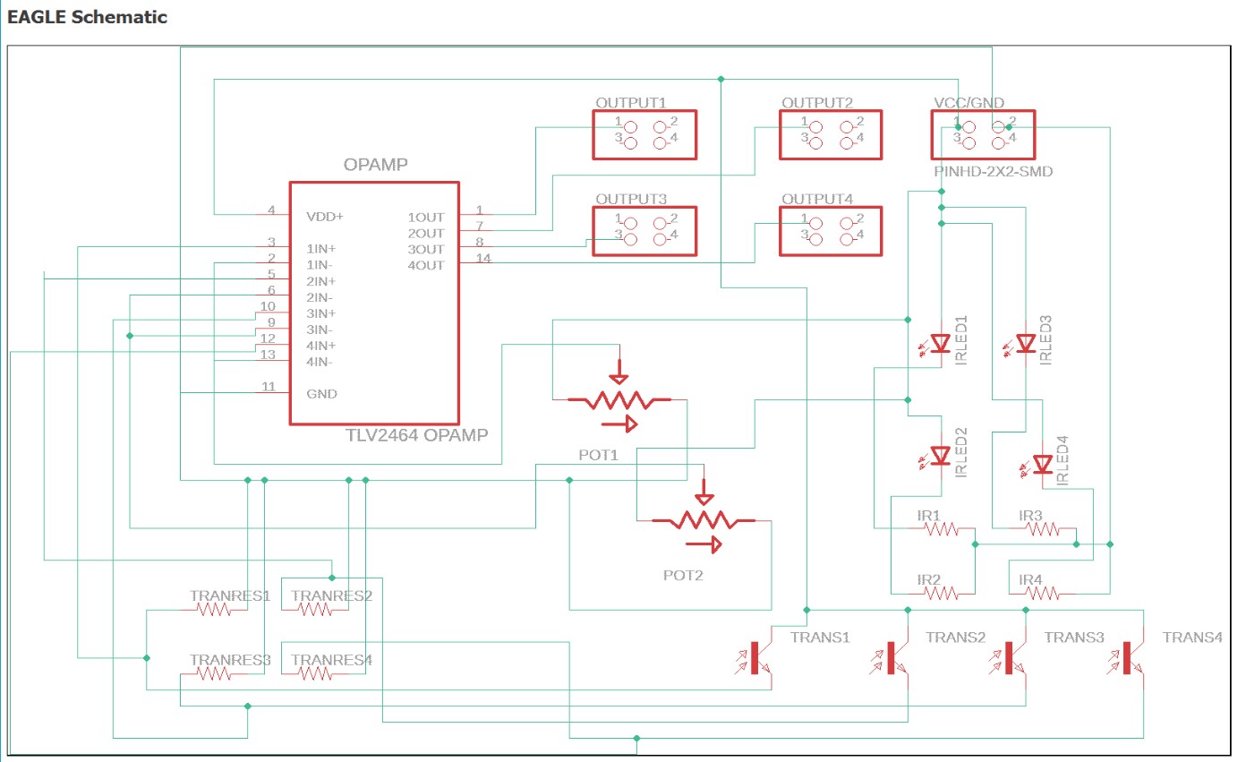
My boards for the control box will be using the TLV2464 Op-Amp chip to tell when a sensor is activated, they will all have these trim potentiometers to set a reference voltage for the op-amp chips to use, they will have corresponding infrared LEDs and infrared phototransistors which can be found here and here. Also, they will have various resistors for each of the diodes that can all easily be found in the lab, and each board will have two 4 pin headers, one for power/ground and one for the output signals going to the wall display.
Gallery
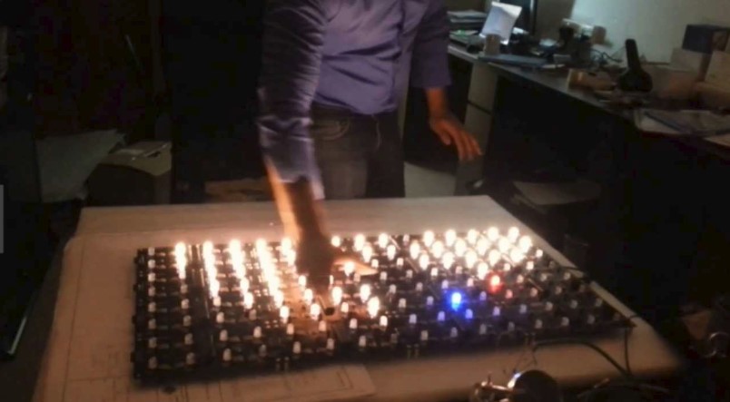
This is an example image that shows a project similar to what I want to do, only mine would be much more design focused.
From Youtube
3D Models
Another thing I wanted to do just for the sake of better comprehension on my part was to create a 3D model of what my project might look like. I used Fusion 360 to make this model and I uploaded it through Sketchfab.
Final project Fabrication Documentation
This part of the page shows the actual creation of each of the parts for my final project. Everything here has been written since 5/28/2019, that’s 21 days before the final project is due.
First Board Prototype
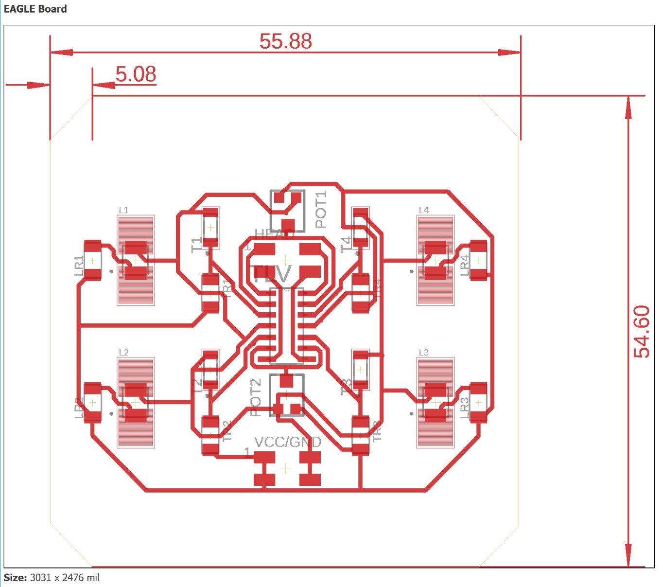
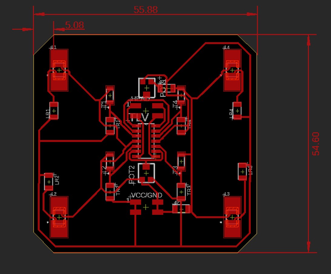
For the circuit boards that will go into the project, I have been working on that along the way ever since week #7, where we learned about board design. I made these schematics and board files some time ago, but after coming back to them I’m not to sure how effective they will be.
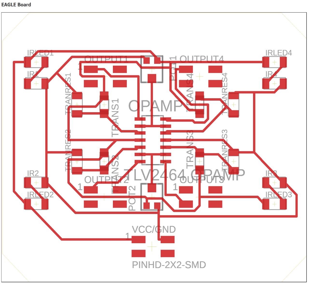
Here are some revised boards that I made up a few weeks ago. The first set of schematics and boards would be for the control box, and the second would be for the wall display.
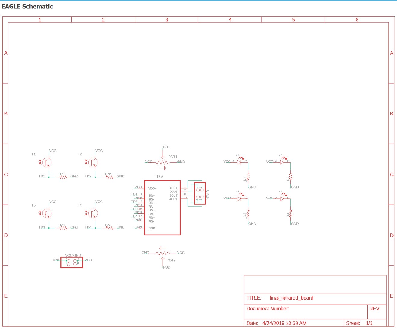
At this point, I’m ready to start trying to make my first functional prototype. I only want to have one working circuit, so I wont be soldering the full board, but I’m going to use one of the above boards to set up a single circuit for a single LED.
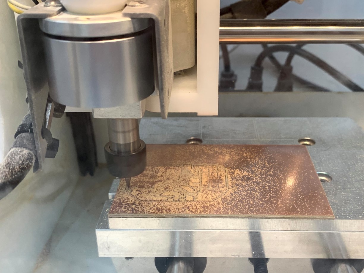
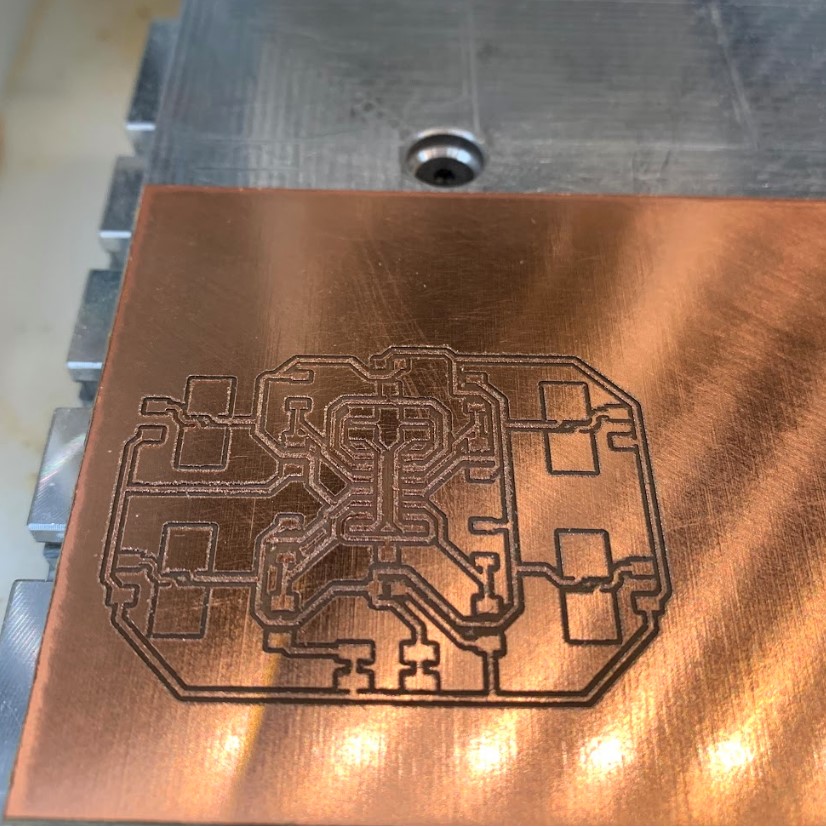
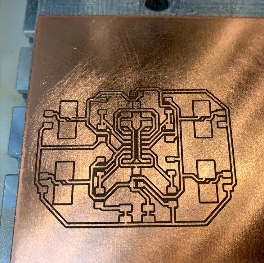
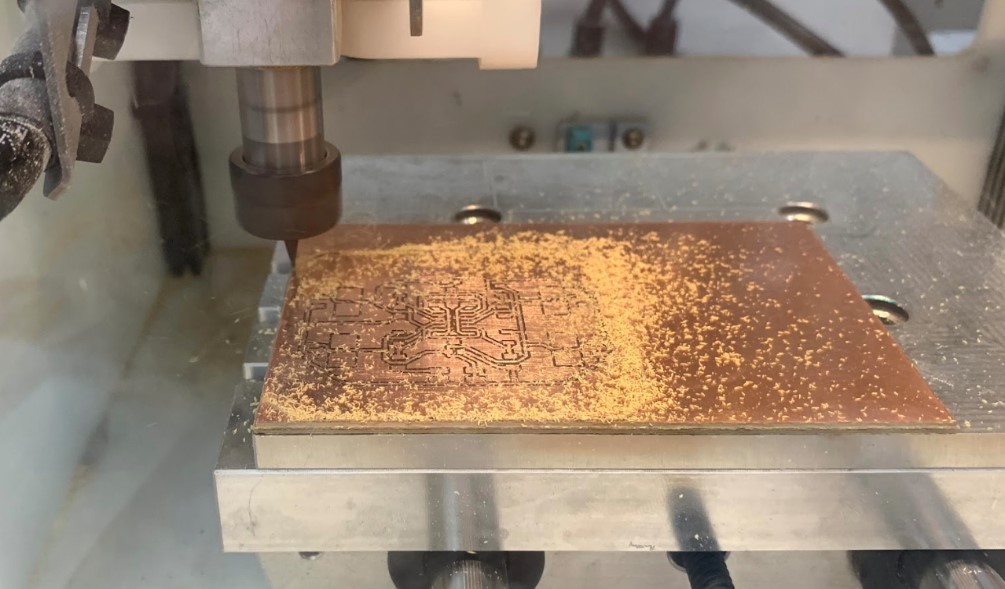
Milling the Board
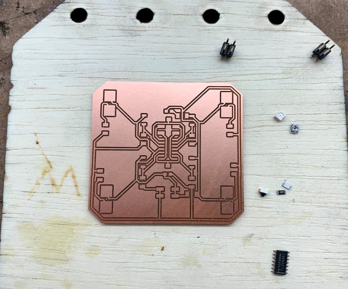
I got a board milled out pretty quickly after this. I’ve documented all about board how to fabricate boards here, so I won’t go into to much detail again. I did, however, take pictures of the steps along the way, which I will include below.
Soldering the Board
I’ve also done a lot of surface mount soldering in the past, which you can find documentation about here, so I won’t go into too much detail again here.
When I made the board file in Eagle, I had to add in new libraries for the components that I was going to order and then use later on. I wanted to visually confirm that all of the components were the same size as the component files that I used in eagle, so I put each of the components onto the board directly just to be sure. Thankfully, everything lined up and looked to be the right size.
Then I got to work with the actual soldering. In the end, the board looked kinda empty, but that’s just because I only soldered down one circuit out of the four that would eventually go on each board.
I got everything set up for soldering, only this time I had to use a spare piece of plywood rather than a tile because I couldn’t find any tiles.
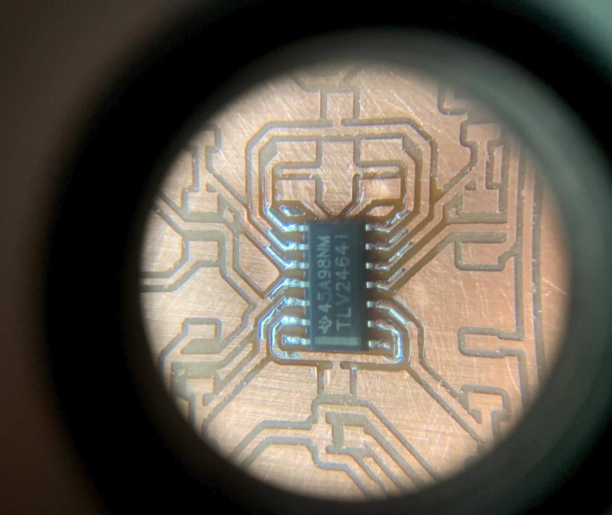
I put down the chip first, here’s a cool view of it through a jewelers loop.
Then I got the rest of the components put down.
I wanted to test out the circuit to see if things were working as expected, so I wired it up with an arduino as a power source and I connected an led with a resistor to a breadboard which then ran the output pin from the chip to it as the power for the LED. That was all pretty confusing to read now that I think about it again, so basically what I did was set up the board so that a yellow LED would turn on when I waved my hand over it.
It didn’t work. No matter how hard I waved my hand or how much I adjusted the potentiometer to change the reference voltage, The LED wouldn’t turn on. I even tried it in a darker room to keep any ambient light from affecting it, and it still didn’t work. Needless to say, I felt like I was at a loss for what to do.
It took me around a half hour to realize that it wasn’t the boards fault, it was mine. I had been working too fast, and in my haste I made the very careless mistake of soldering the chip on backwards. When I first realized my mistake, it didn’t seem like that big of a deal to me because of how the op-amp chip’s pins were laid out. All that really changed was which one of the four OP-amps in the chip I was actually using. The issue, really, was that I had the power and ground flipped to the wrong pins. No wonder it was getting so hot.
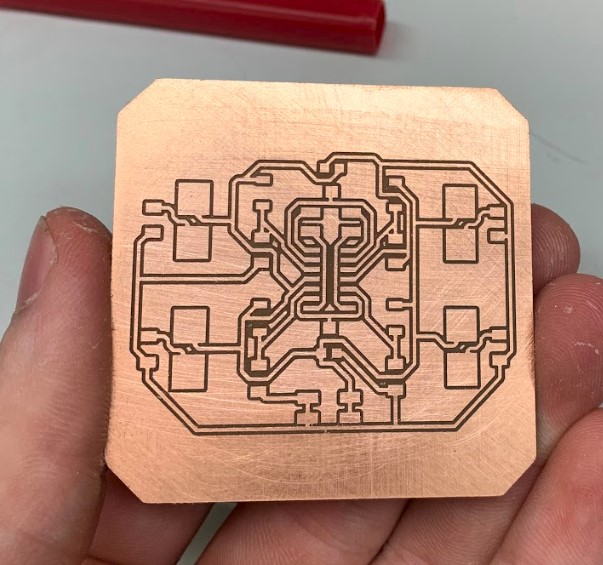
I milled out another board, same as before, and got it soldered correctly this time.
Then I got everything connected again so that the yellow LED should turn on if the circuit is working properly.
Aaaaand it still didn’t work. On the bright side, the chip didn’t seem to be getting nearly as hot as before, but regardless the circuit still wasn’t working as expected. At this point, I was starting to question if I even had the voltages correct so that the circuit could work the right way, so I got out a multimeter and started measuring stuff.
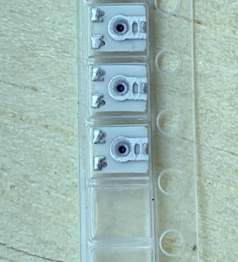
When I was measuring the potentiometer, I noticed my first sign of odd behavior. No matter how much I changed the potentiometers value from 100 ohms all the way to one megaohm, the voltage passing through didn’t drop at all. It stayed at a constant 4.95 volts. This was around the time that I noticed the second sign of odd behavior, literal smoke coming up from the potentiometer whenever I set it to the highest resistance. I quickly disconnected the board from power, but the damage had been done and the potentiometer was fried.
Honestly, though, I’m glad the potentiometer burned. Without that happening I probably would have kept on going thinking the issue was something else on the board, (and it very well could be something else entirely, but right now my next step is to fix the potentiometer issue and try again).
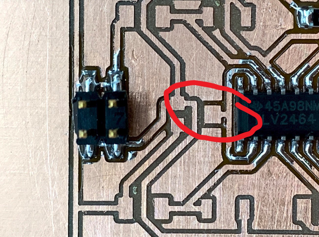
So at this point you may be saying to yourself, “yeah, the potentiometer started smoking and that means it’s not working properly, but why was it smoking in the first place?” I’m glad you asked. The cause of the issue was basically just bad board design that led to a short circuit. I didn’t know that the potentiometers front lead extends about halfway down underneath the bottom of the component, and because of this, I made the board design with a different trace passing underneath the component. I thought that the space under the potentiometer was free real estate, but really it was already being taken up by the wiper pin on the potentiometer.
It’s kinda hard to visualize without a point of reference, so here’s a few pictures. The first one shows the bottom of the potentiometer with the wiper pin in the middle of it, and the second shows the footing of the component on the board that has the other trace routed directly below where the wiper pin extends out to.
My next step will be to make an updated board that doesn’t have this issue. I’ve included a picture of it below, and you’ll notice that not only have I changed the traces for the potentiometers, I’ve also added in two jumper resistors to help me fix the initial problem, and I’ve spaced out the IR LEDs more to keep them from triggering the phototransistor too early.
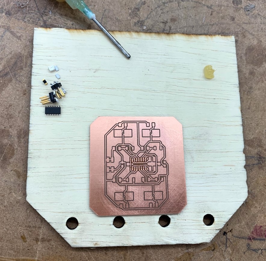
I got this new board milled out with out any issues, then I got it set up to start soldering.
Once again, I only soldered on one of the four circuits that would eventually be on the board so that I could see if even one of them worked before moving on to the rest.
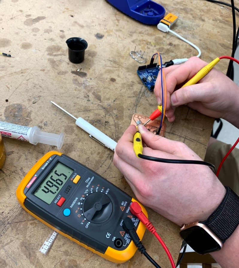
Next, I started using a multimeter to check all of the voltages across the board to be sure things were working as expected. This led me to discover my next problem, even though I got rid of the conflicting trace beneath the potentiometer, there was still exposed copper underneath it that just hadn’t been milled away yet. This caused the potentiometer to still not work as expected, because when I measured the voltage off of it at its highest resistance, (1 megaohm), it still ended up reading a solid 4.965 volts. For reference, it should have been somewhere closer to about .5 volts or even lower.
This was pretty annoying, because it basically meant I had just soldered and designed a new board to get the same failing result. I had one more idea at this point, though. I knew that in Bantam Tools, the software that actually converts the .brd file into workable G-Code for the othermill machines, there was an option to increase the trace clearance for the whole board. This helps to reduce the amount of unmilled copper sitting on the board by adding a buffer zone of at least 1.5 mm in my case around any traces or pads on the board, meaning that the copper underneath where the potentiometer sits would be milled away with the rest of it.
Here you can see what this increased clearance actually looks like in Bantam.

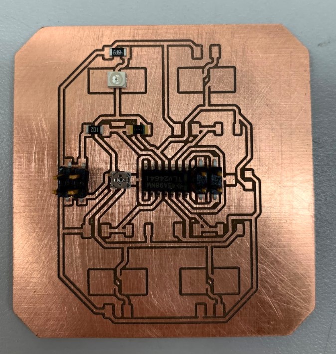
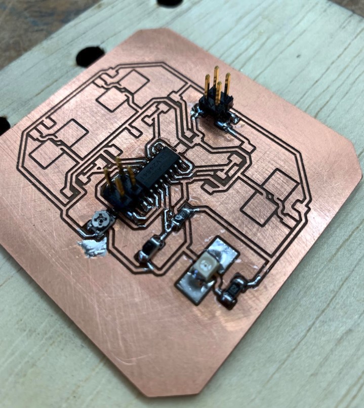
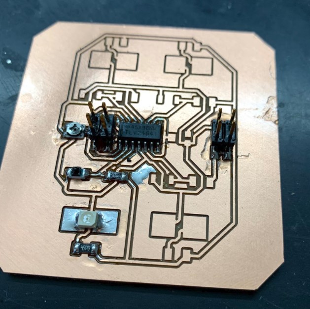
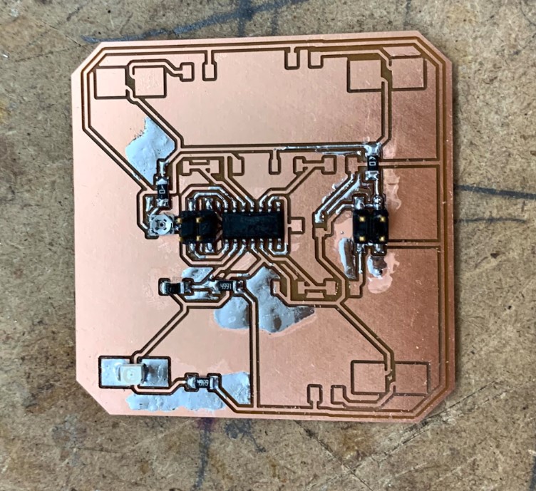
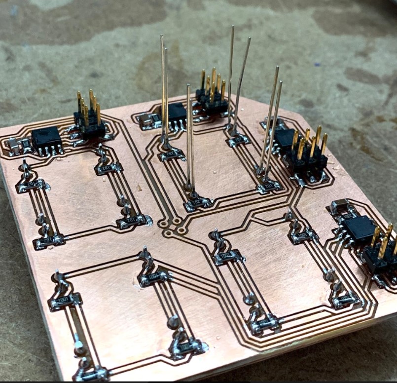
I got this new board milled and soldered, and it ended up looking really clean.
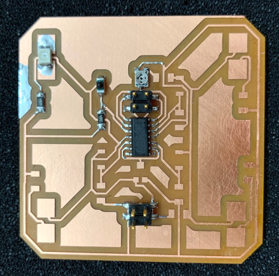
It’s working!
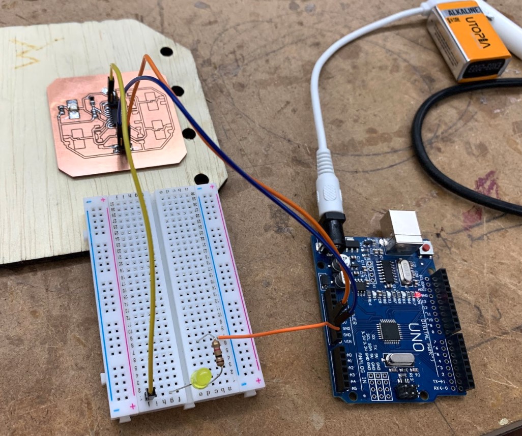
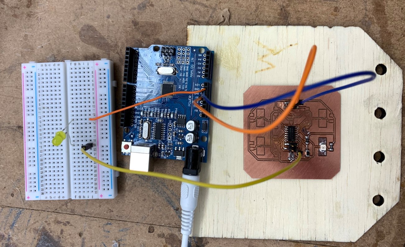
I connected the board to an arduino as a power source and a breadboard with an LED that was basically a stand in for the eventual wall display that I will make. When I tried it this time, I was incredibly happy to see that it actually worked very well.
This was a pretty big milestone for my project. I finished up that much of the board right before we had to leave the lab for the day, so I couldn’t work on it any more there. Once I got home, though, I was able to solder the rest of the components onto the board and have a fully working board with four functional infrared circuits.
Board Revisions
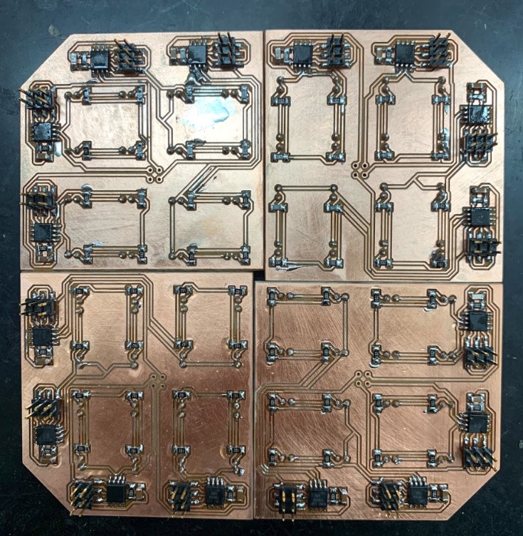
The board design doesn’t stop there, though. I wanted to make one more change before I considered this part of my project “done”, and it was pretty simple to edit in. Rather than using top mounted pins on my final boards, I wanted to use pins that came out from below the board so that the wires and such wouldn’t get in the way of the functionality of the circuits. All this really meant for me was changing the component from a surface mount header to a through hole header in my board files, and that was that.
I milled out this new design and got it all soldered again, and the result was a much less cluttered appearance for the outward facing part of my board.
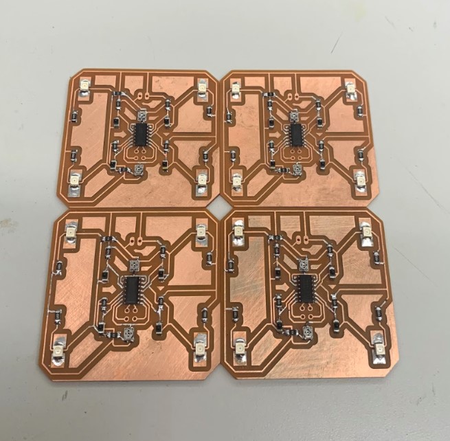
In the end, I needed to have four of these boards all ready to go for my final, so I got to work the next day on cutting out and soldering four more of these boards.
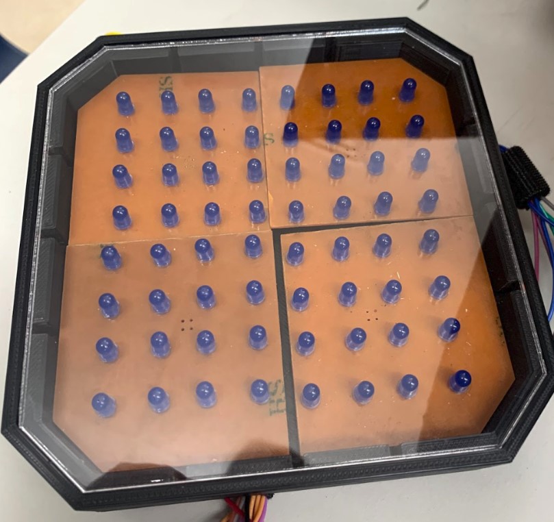
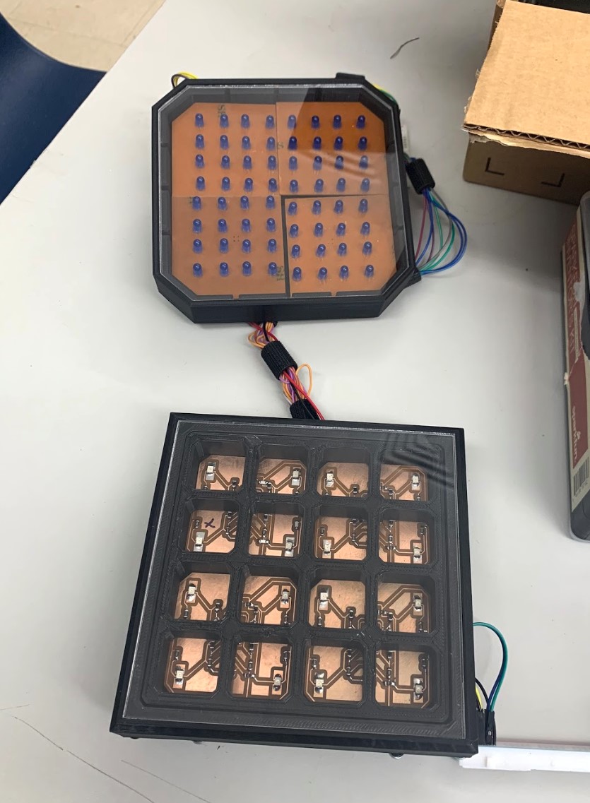
Designing the Wall Display Board
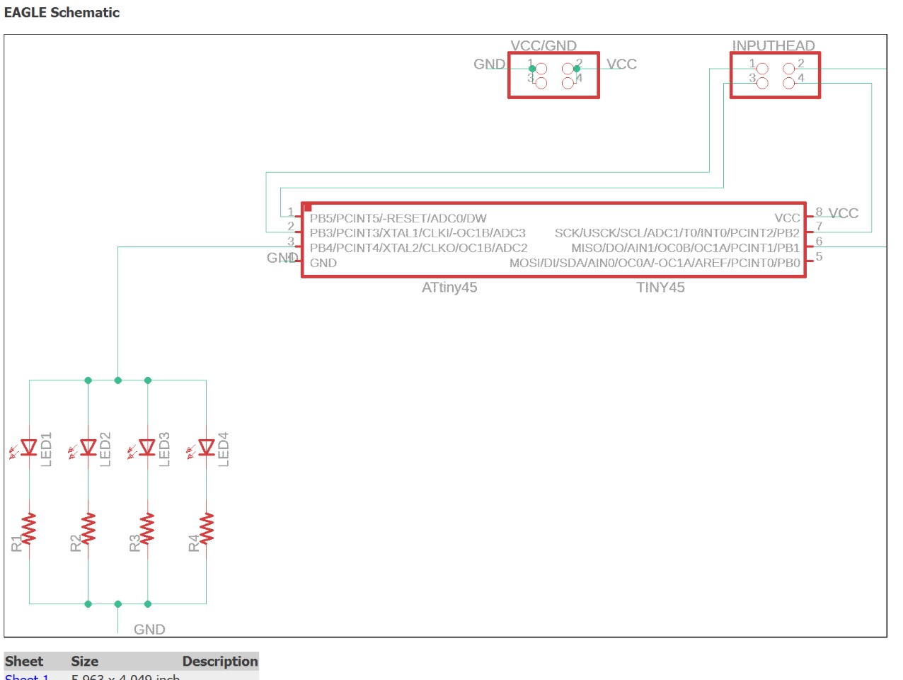
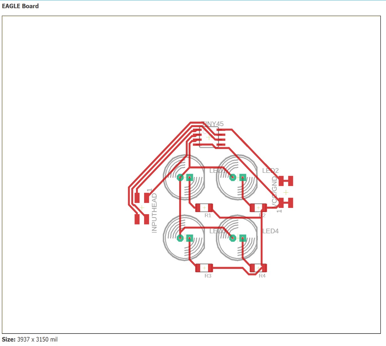
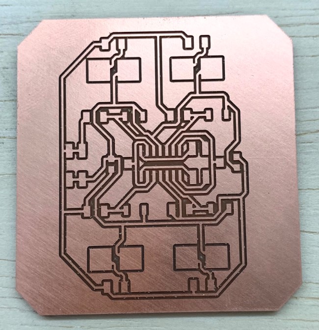
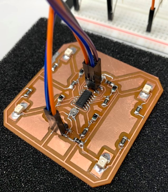
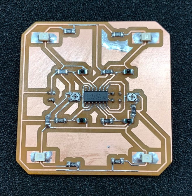
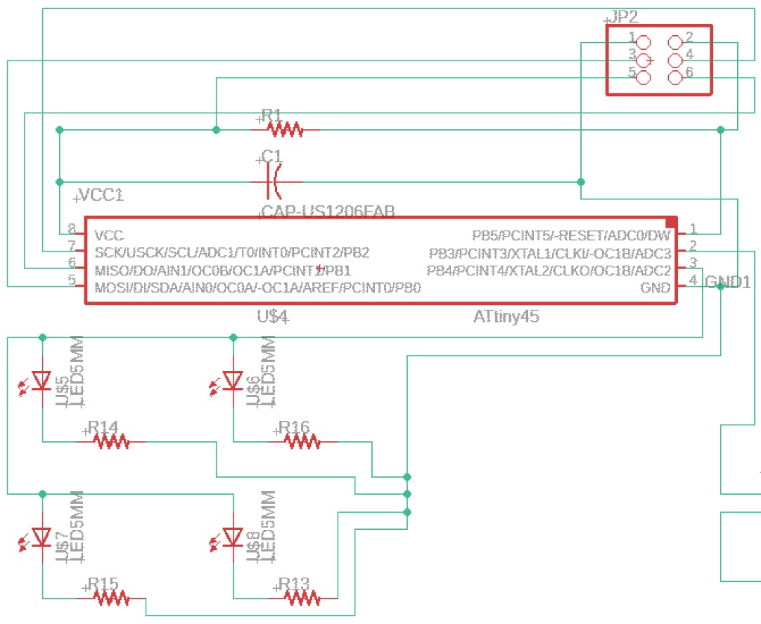
That wasn’t the only board I would be using in my project, though. I also needed one for the wall display that would hold all of the LED lights as well as the attiny45 chips that let me include embedded programming. I went back over into Eagle and got another schematic opened up for this.
It took a little while, but after some time working with it I had a schematic made for the board. It looks pretty big at first, but you’ll see that it’s really just four of the same schematics on one board.
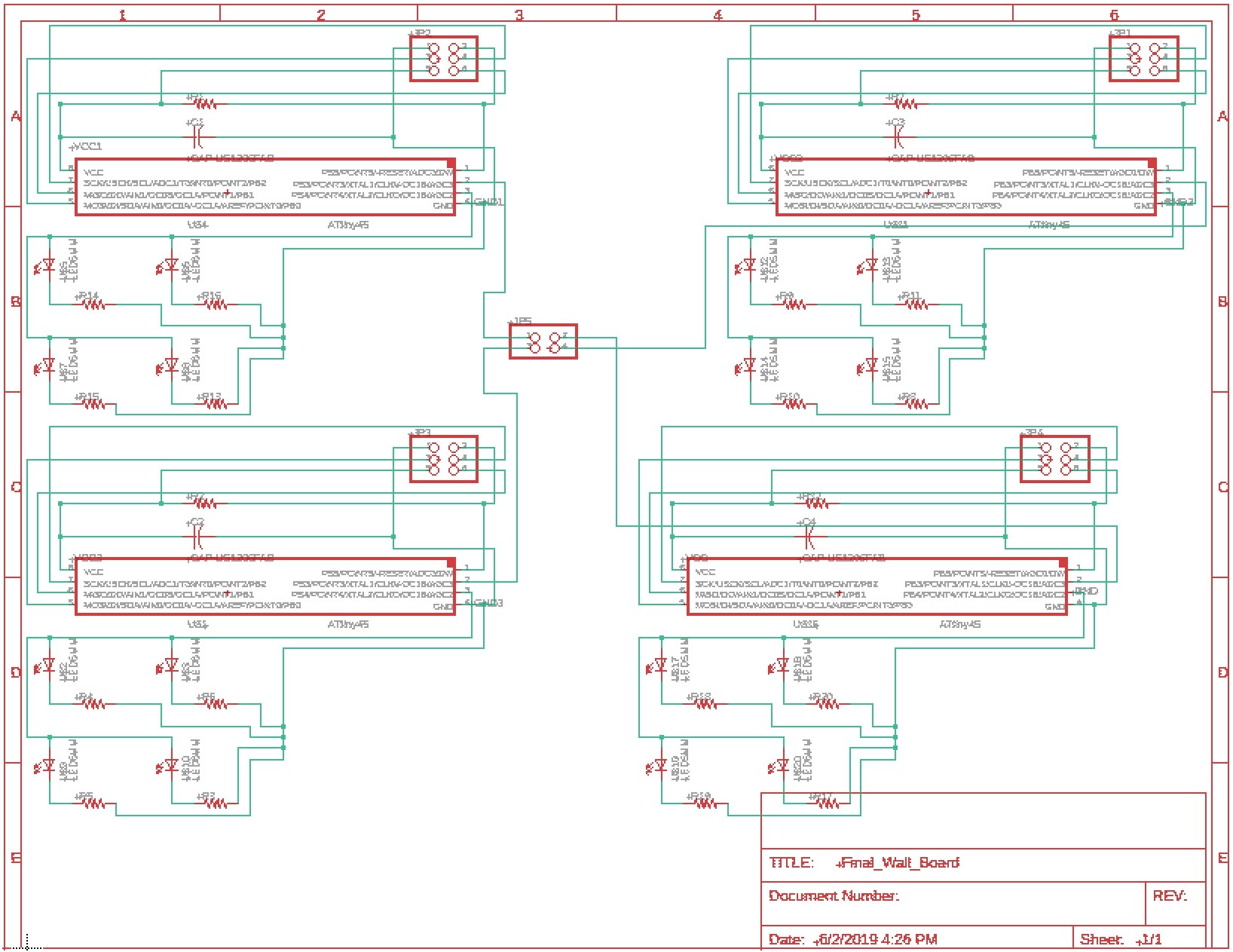
Then I made the board file from the schematic.
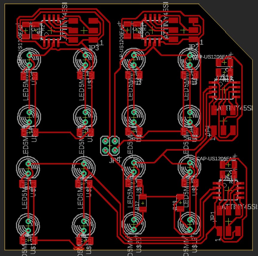
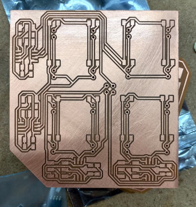
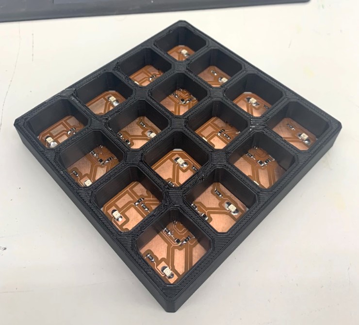
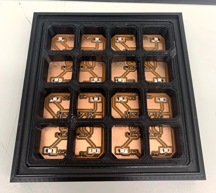
Then I milled out four of these boards because I would need four for the final result, and I got them all soldered that day.
The wall display board ended up being much more troublesome than I first expected. My plan originally was to just solder wires directly into the holes on the board to make my connections, but after actually trying this just once, I realized the issue. The wire, (I now know it is because it was a solid core wire), was too stiff to dispel any tension built up on the wire, and this meant that when I was moving the board around with the long wires attached, it was allot more likely that the wire would break free from the hole in the board and tear up the copper traces. This tearing up of the traces would prove to be one of my main problems by the end of the project.
I had a lot of trouble with this, and in the end I realized I could just be using stranded core wire instead, which is much more flexible and didn’t break any of the traces at all.
Another issue that I ran into a bunch for this board was that the LED’s broke off verrrry easily. It was pretty much the same problem I was having with the data wires, but to a lesser extent. Due to this issue, you’ll notice that one or two of the LED’s on the final probably won’t work, but it should still be enough to get the broader idea across.
3D Printed Part
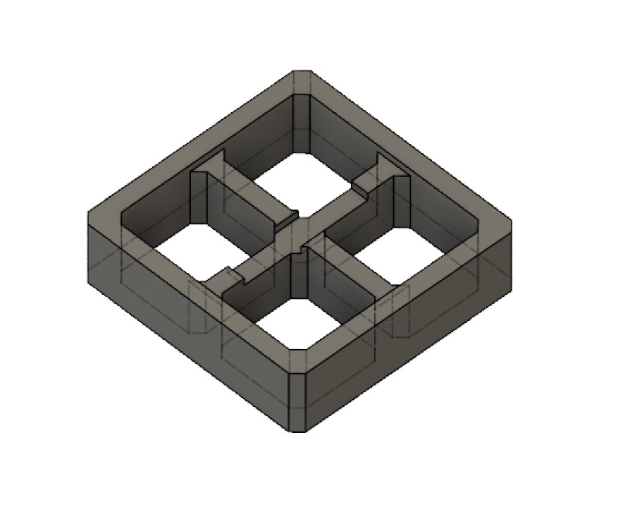
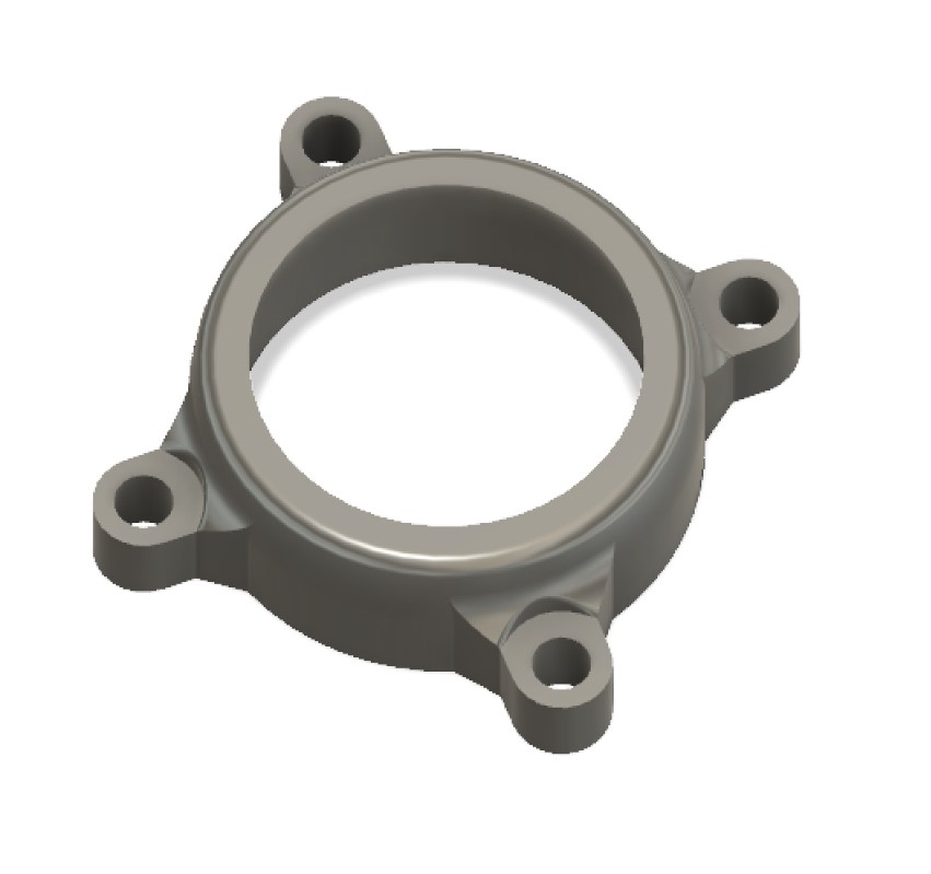
As you may have noticed in some of the videos above, the board has trouble working correctly when light from one of the LEDs hits the sensor from an entirely different circuit. I expected this to happen, so I have slowly been thinking about how to resolve the issue along the way, and I thought that 3D printing a specific part that fits onto the board and separates all four circuits from each other would be a good implementation of my 3D printing skills for my final project.
CAD Design
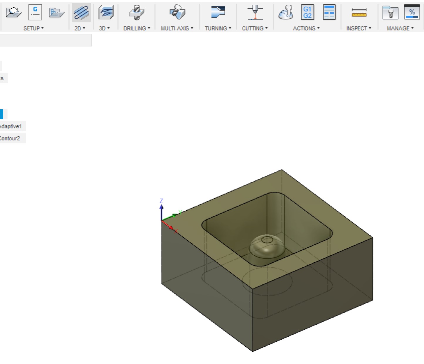
The goal is to have a small printed part that will fit over the board and separate it into four different “quadrants” if you will, so that the IR light from one circuit does not activate the phototransistor on the circuit next to it. To print this part, I’ll first have to make a CAD file for it, and I plan to do that in Fusion 360.
I opened up what is now one of my favorite softwares, and this was the first rough estimation I came up with.
3D Printing
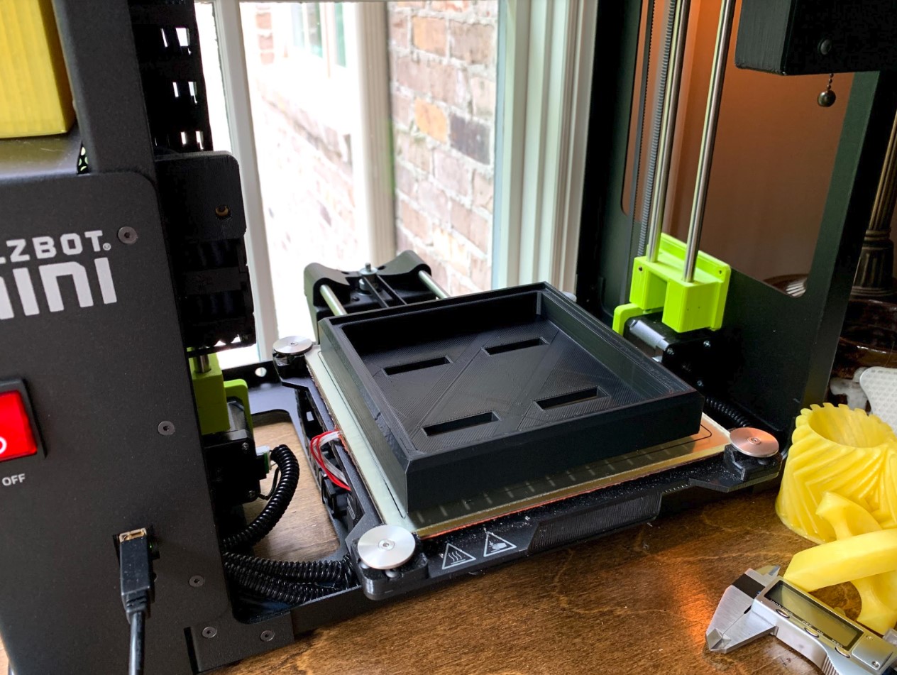
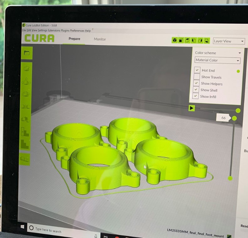
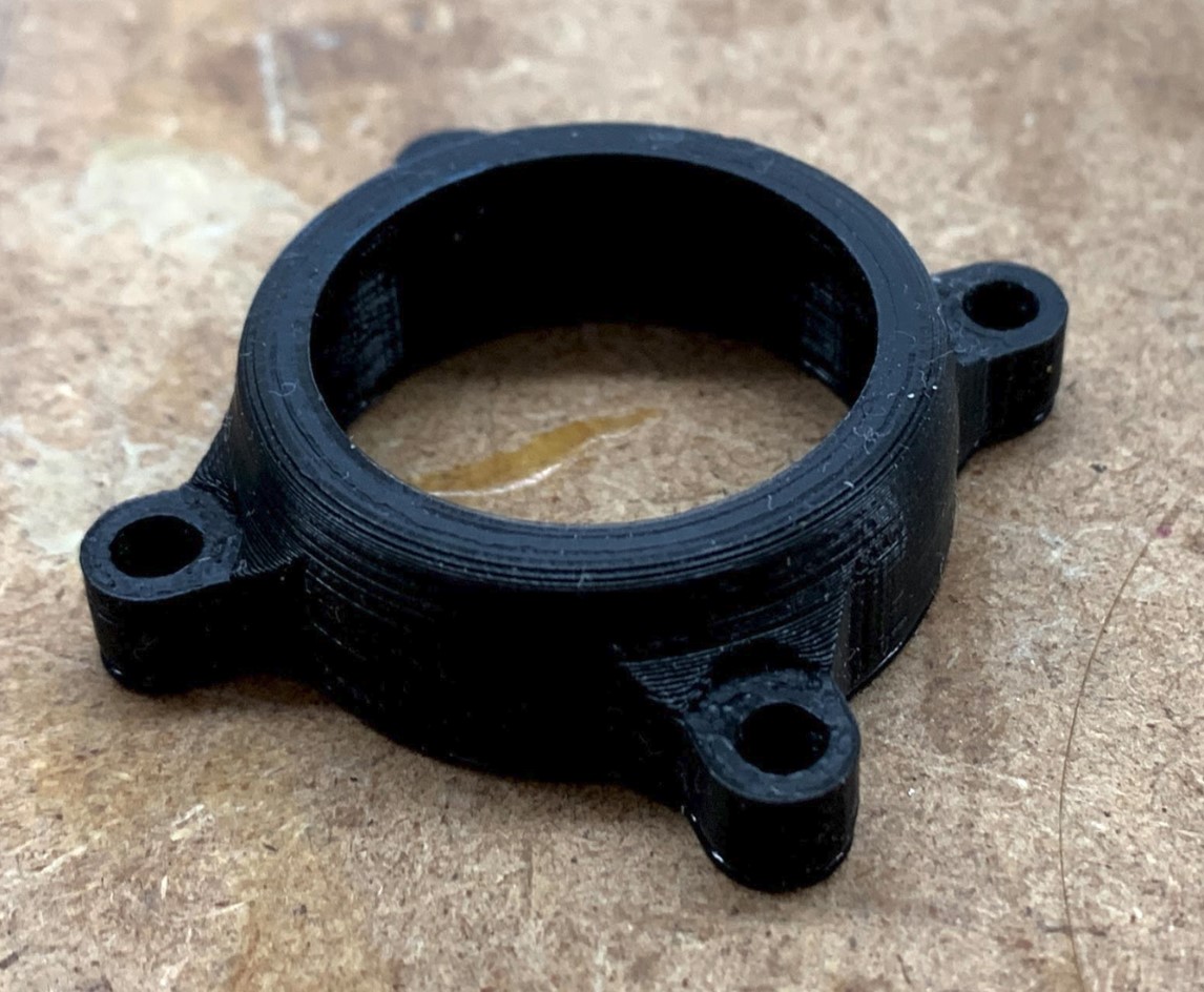
I’ve done a lot of documentation on 3D printing here so I wont go into too much depth on this page as well. I printed this out in white ABS on a Lulzbot Mini 2 machine, and it came out quite nicely. I chose to print this in white because I knew that the color white reflects all other light, and my goal was for the white walls to increase the sensitivity of the board by reflecting the IR light outwards.
In actuality, though, the white color of the 3D printed part was too reflective, making it so that the circuit would activate just from having the part placed around it.
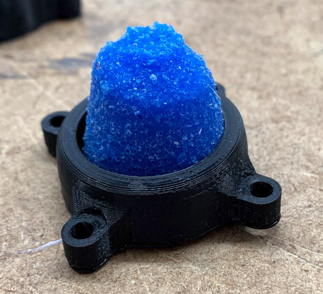
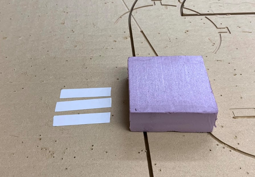
I figured that I could try using black PLA for the part rather than white so that it wouldn’t be as reflective, but I wanted to test this idea first so that I wouldn’t just be wasting PLA if it didn’t work. I cut up some black paper and placed it into the slots to see if my board would work correctly this way.
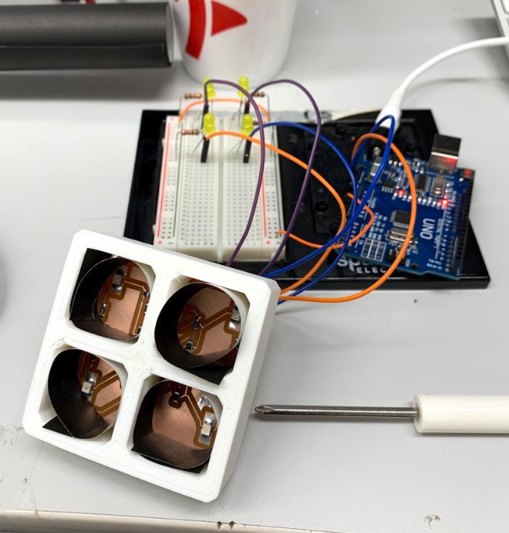
With the black paper in place, my board was working as expected.
Next, I printed out the part again in black PLA.
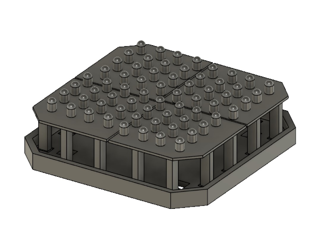
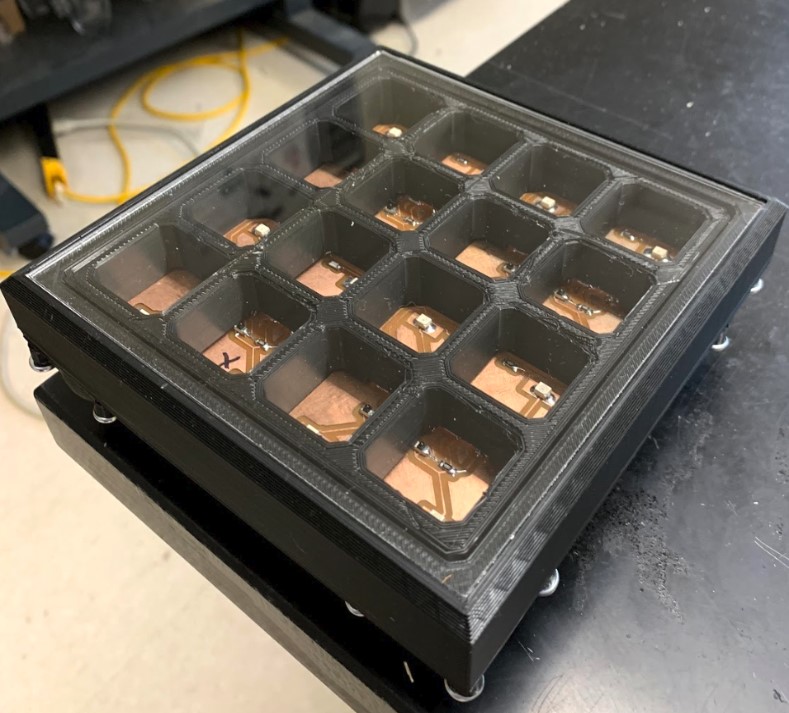
My next step from here was to make a part that would hold all four boards at once for the final result, so I went back into Fusion 360, used the original part to create a rectangular pattern array with all four, and joined the four bodies together as one to create a larger mount.
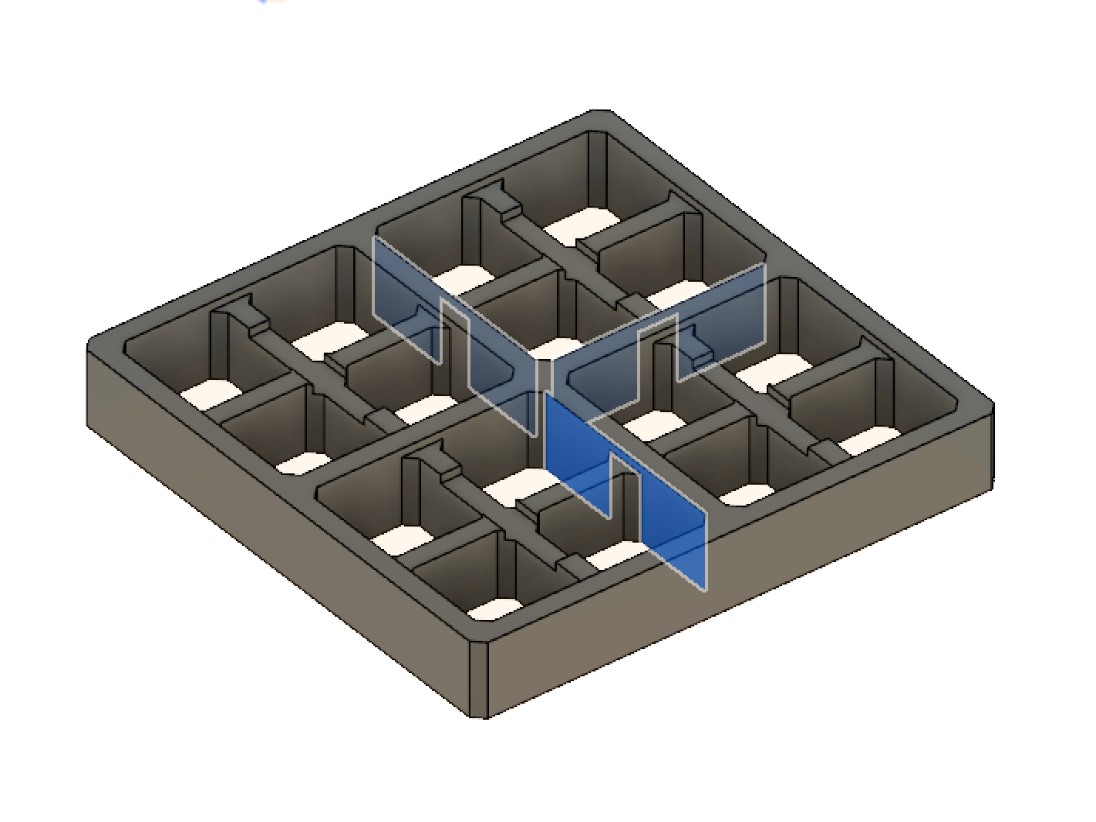
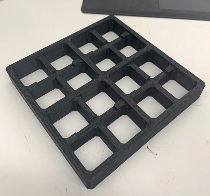
I got this other part printed out next, and it came out nicely as well. All of my boards fit in there perfectly.

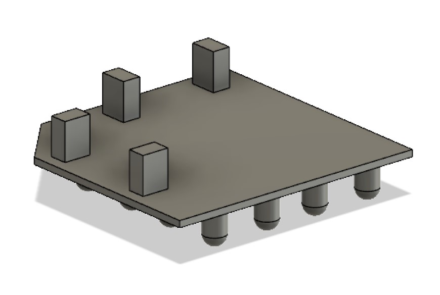
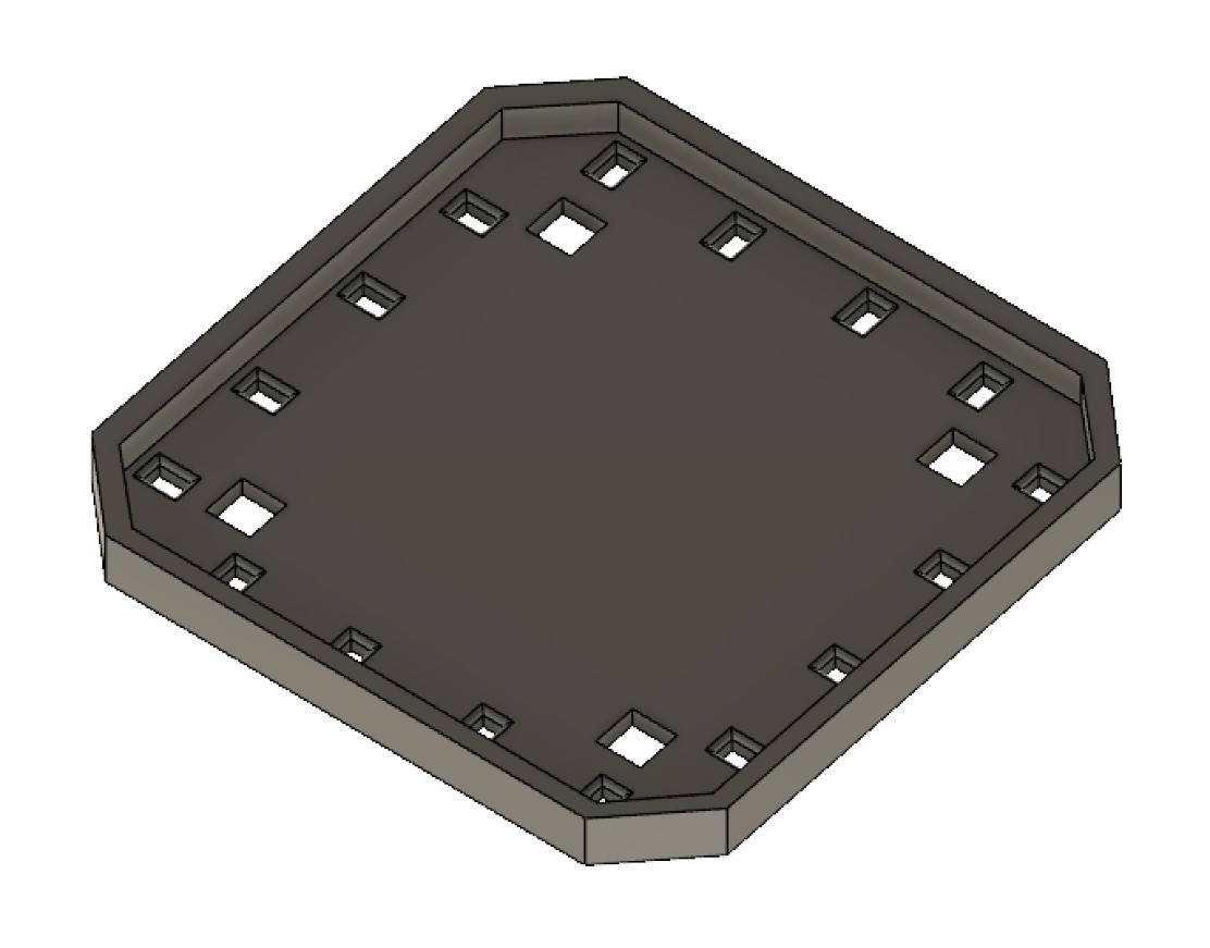
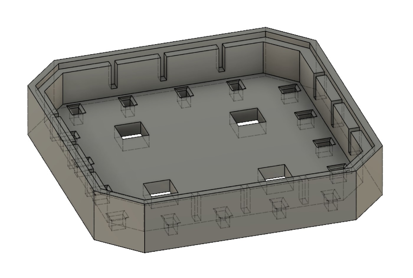
Next up, I wanted to make a mount for this mount that would act as the final exterior for the control box while also giving it a good place to hold the acrylic sheet over the top. I went back into fusion 360 to make this, and here’s what I eventually came up with.
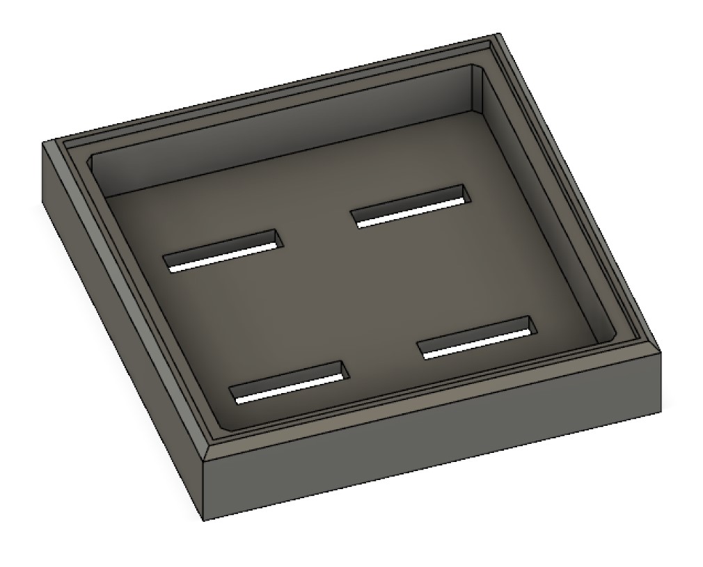
I got it printed out, and it held the other mount in place perfectly.
Second 3D Printed Part
I had one other set of 3D printed parts for this project, all of the mounts for the LED boards. It took me a little longer to get a working mount made for these boards because of how the dimensions were each a little bit different, but I was able to make a pretty good one eventually by creating a model of the boards themselves and then using those models to make a second model based off of the first in Fusion 360
I got this new mount printed out next on the Mini 2, and everything fit in quite nicely once it was done.
This isn’t the end of all the iterations of my 3D printed display mount. I ended up making one more change and that was adding a cutout along the top to put down an acrylic panel to protect the electronics beneath.
Even More Printing
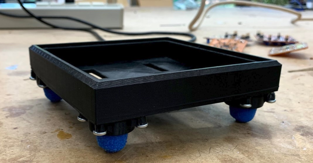
As you’ll see in the next section following this one, I used molding and casting to create four soft “feet” for the control box of my project. This presented the challenge of somehow attaching these soft rubber thimble shaped pieces to a hard smooth plastic part. To overcome this issue, I just did even more printing and made a part that could be screwed into the bottom while securely holding the rubber parts in place.
I have to preface the rest of this by saying that this was not my idea. I got the idea entirely from Maxine, one of my labmates, so I can take no credit for it. All I did was take the idea and resize it to fit my parts.
I modeled it in Fusion 360.
Then, I printed out four of them for the four feet on my project.
CNC and Molding/Casting
Originally during week 10, I spent lots of time making four cast feet for the final result of my light table. Now, since I’m making my final result a lot smaller, The parts that I made previously are going to be to big. Due to this, I’m going to recast four feet for the project, but this time they will be much smaller.
Once again, I have a lot of documentation on how to use the CNC machine to make a mold and then how to make molds and cast parts here, so I won’t go overboard on the documentation here.
Machining the Pattern for the Mold
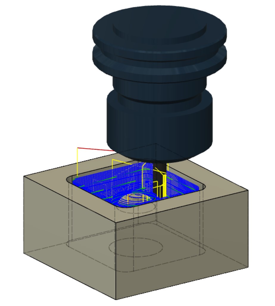
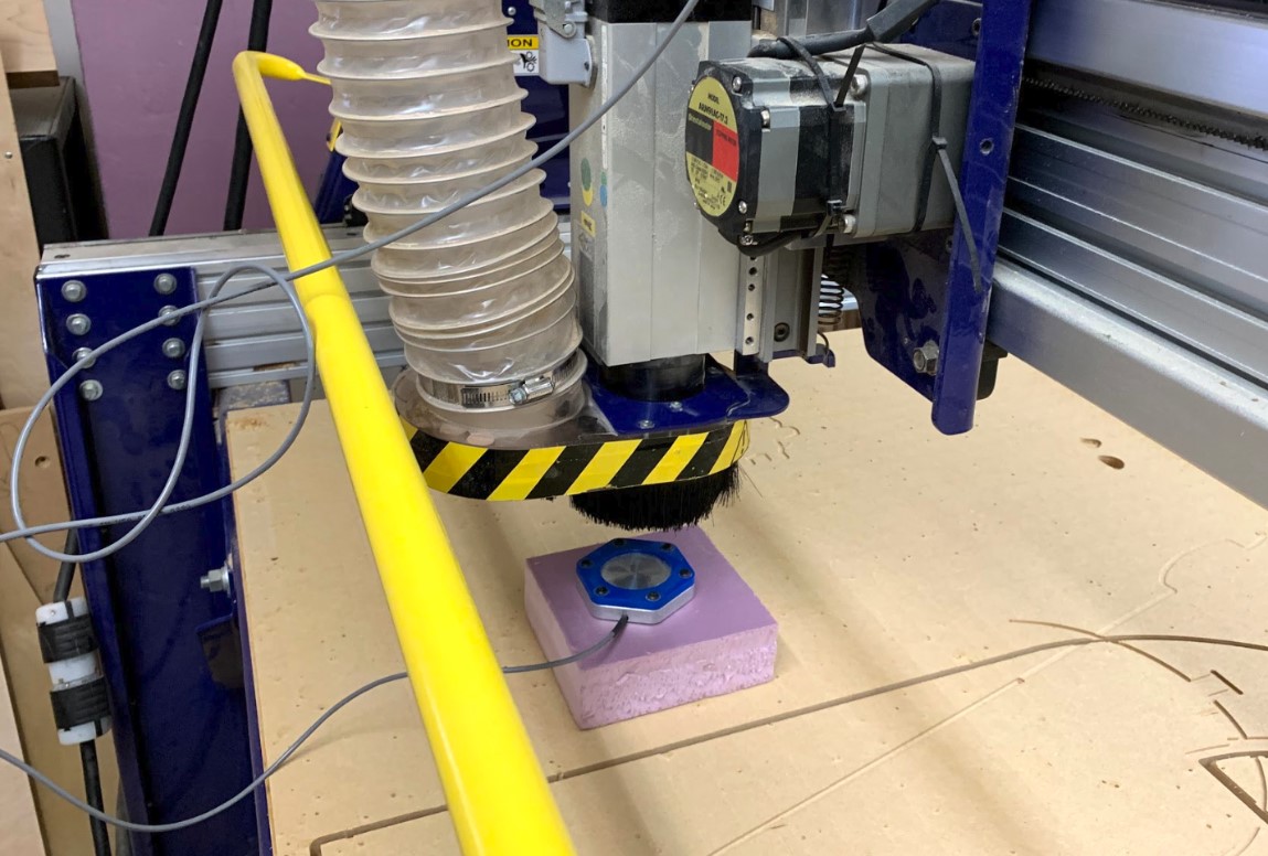
To make the pattern for the mold for my casted parts, I first had to design and mill the pattern on our shopbot. I started in Fusion 360 and made a model of the pattern, then I opened up the CAM environment in fusion once again.
I simulated all of my toolpaths, and once I felt like things looked good I sent the GCode over to the shopbot.
I got a piece of the insulation foam put down, zerod the Z axis off of the material, ran an aircut to be sure it looked good, then I started up the cut.
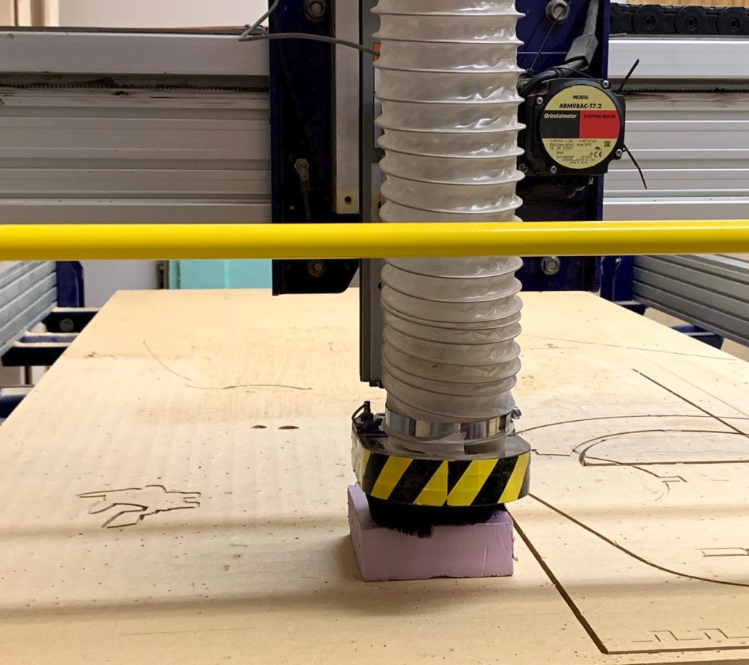
Once it was finished, I was ready to make a mold from the pattern.
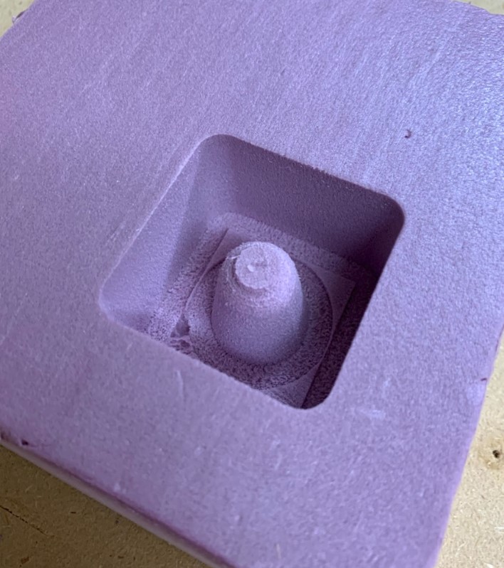
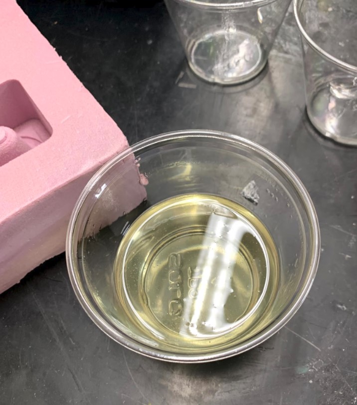
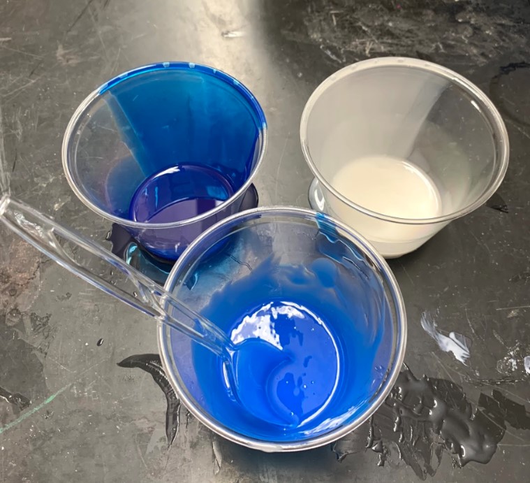
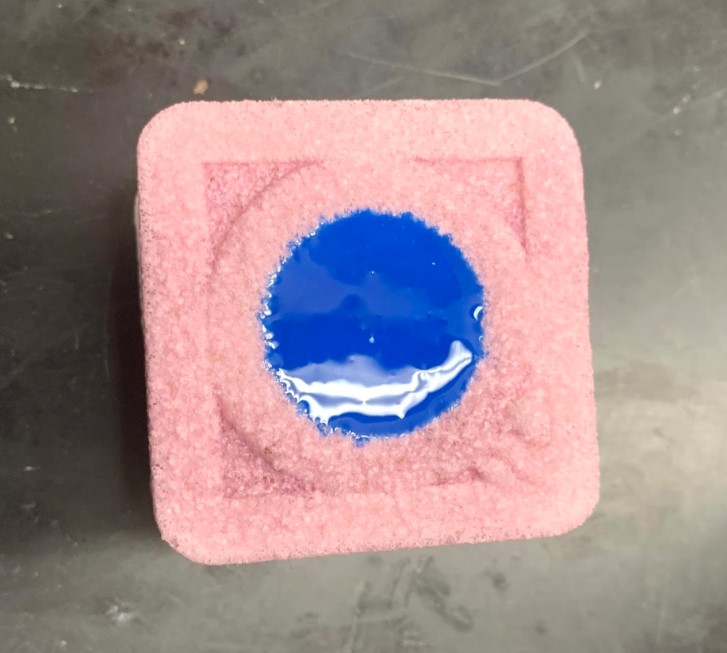
I started by getting out the material I would use to make a mold. I used the Smooth-Cast 300 Bright White Liquid Plastic compound, and to start I poured out equal parts into two cups.
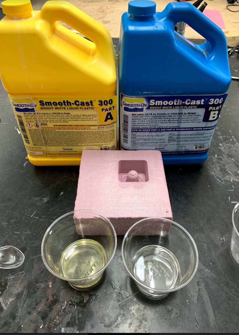
I mixed these parts together and poured it into my pattern. After about 2 minutes the compound flash-cured into hard white plastic in a span of about five seconds.
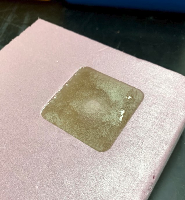
The mold didn’t come out looking amazing, but honestly it didn’t have to. For a small part like mine, the quality isn’t as important as the functionality.
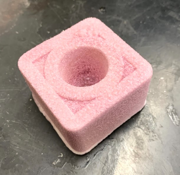
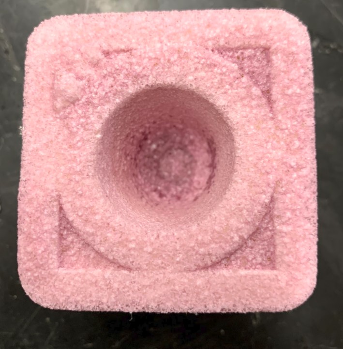
The weird part of this though is that it seems like the heat from the curing process of the mold has melted down the top part of the foam pattern, so it looks like the pattern is unusable at this point.
Casting Parts
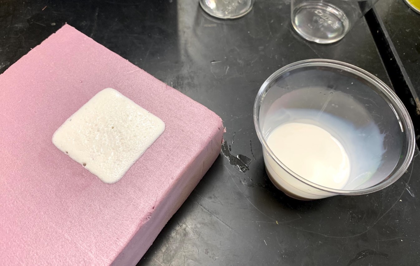
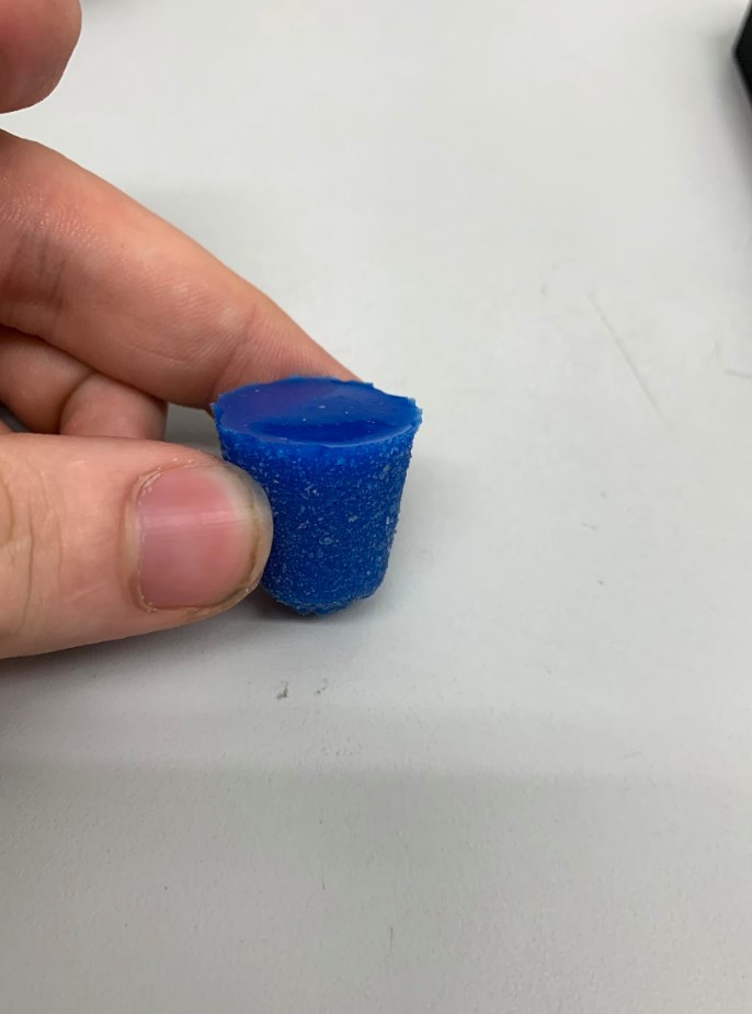
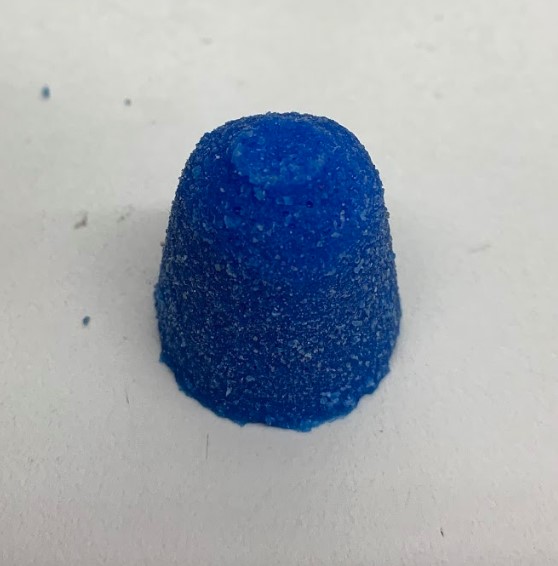
I starting casting parts for this out of the Mold-Star 300 molding compound. I used a soft material as my final pour because the part needs to absorb vibrations at the bottom the control box.
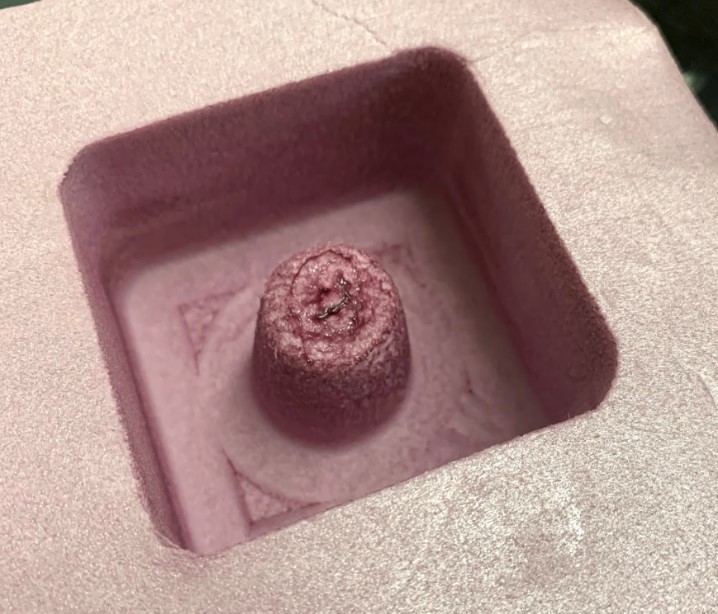
Eventually I was ready to pour this into the mold and make my first part.
After letting it cure overnight, I got it out of the mold and my first cast part was finished.
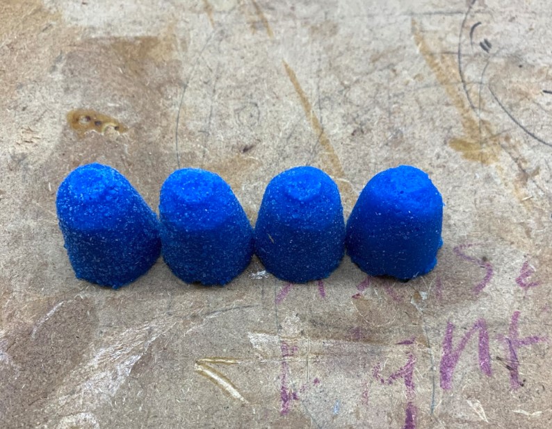
Over the next few days, I kept casting more parts from my mold until finally I had four of them ready to go.
Embedded Programming
This actually didn’t end up being as much of a challenge as I expected it to be when I began this journey so many months ago. First off, I will admit that the only reason I really used programming at all in this project was to get it into my final project however possible so I could include it as one of my design units. The circuit would still be fully functional without the chip and the programming, in fact all I would have to do is change around some various wire connections and I could use it right now without the chips.
That’s not what this is about, though. It’s about showing that I know how to use embedded programming, not necessarily in the most effective way, just in some way. That’s why for my embedded programming function, I used an Attiny45 chip to tell when one pin was receiving an input of high, and to then output a high signal on a different pin when this happened. I could just rout the high signal coming from elsewhere directly to the traces that the chip outputs to, but then I wouldn’t need any programming :).
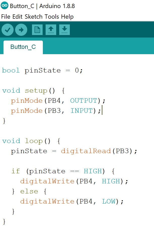
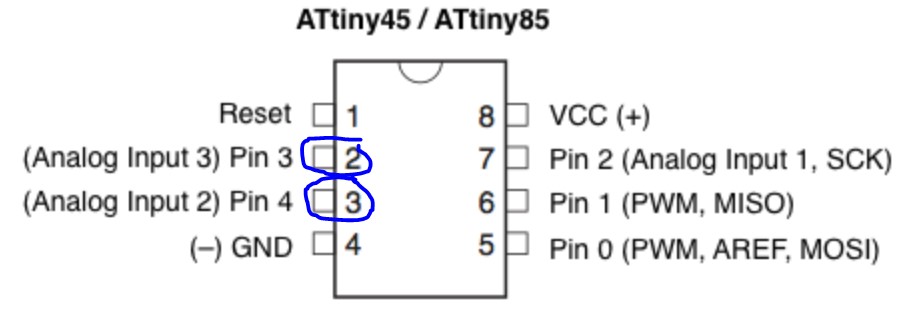
I started by identifying the pins I would be using. According to my schematic, they were the two pins in the middle of the right side of the chip.
Then, I found the pinout for the Attiny 45 chip and realized that these were pins PB3 and PB4.
Then, I opened up the normal arduino button example as a starting point since it used “if” statements, and changed around the pin values to match those that I would be using.
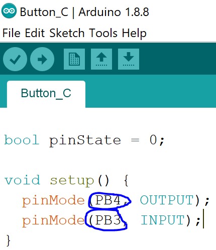
Then, I was eventually able to manipulate this code into working for my project so that when the input pin received a low signal, the LEDs were off, and when the input pin received a high signal, they were on.
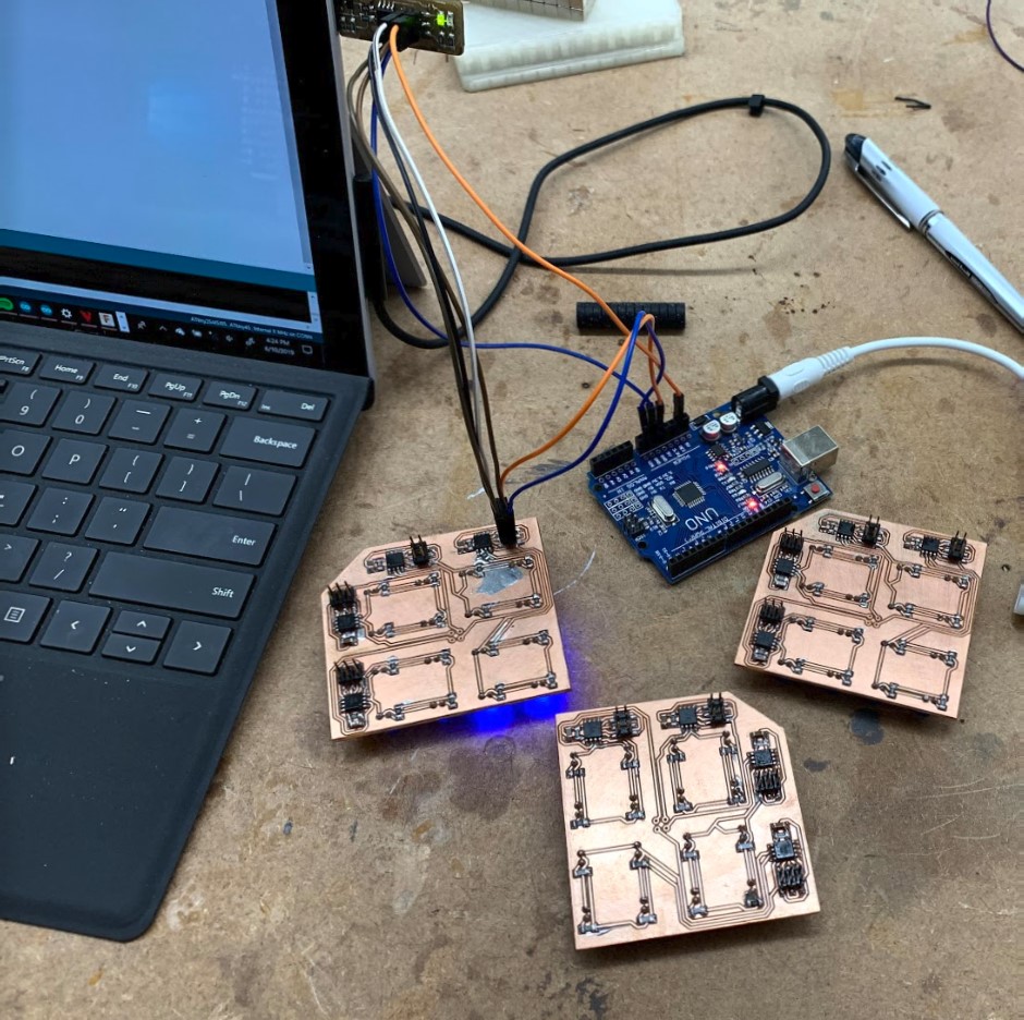
I programmed all of the chips on the board next by attaching my programmer that I made for electronics production week and sending the code through the arduino IDE. I have more details on this process documented here.
The programming process itself looks a little crazy, but that’s only because of all the connections that have to be made between computers, boards, and power sources. I was using an Arduino Uno as my main power source for the board and the programmer since it has two VCC-OUT pins as well as two open grounds.
Laser Cutting
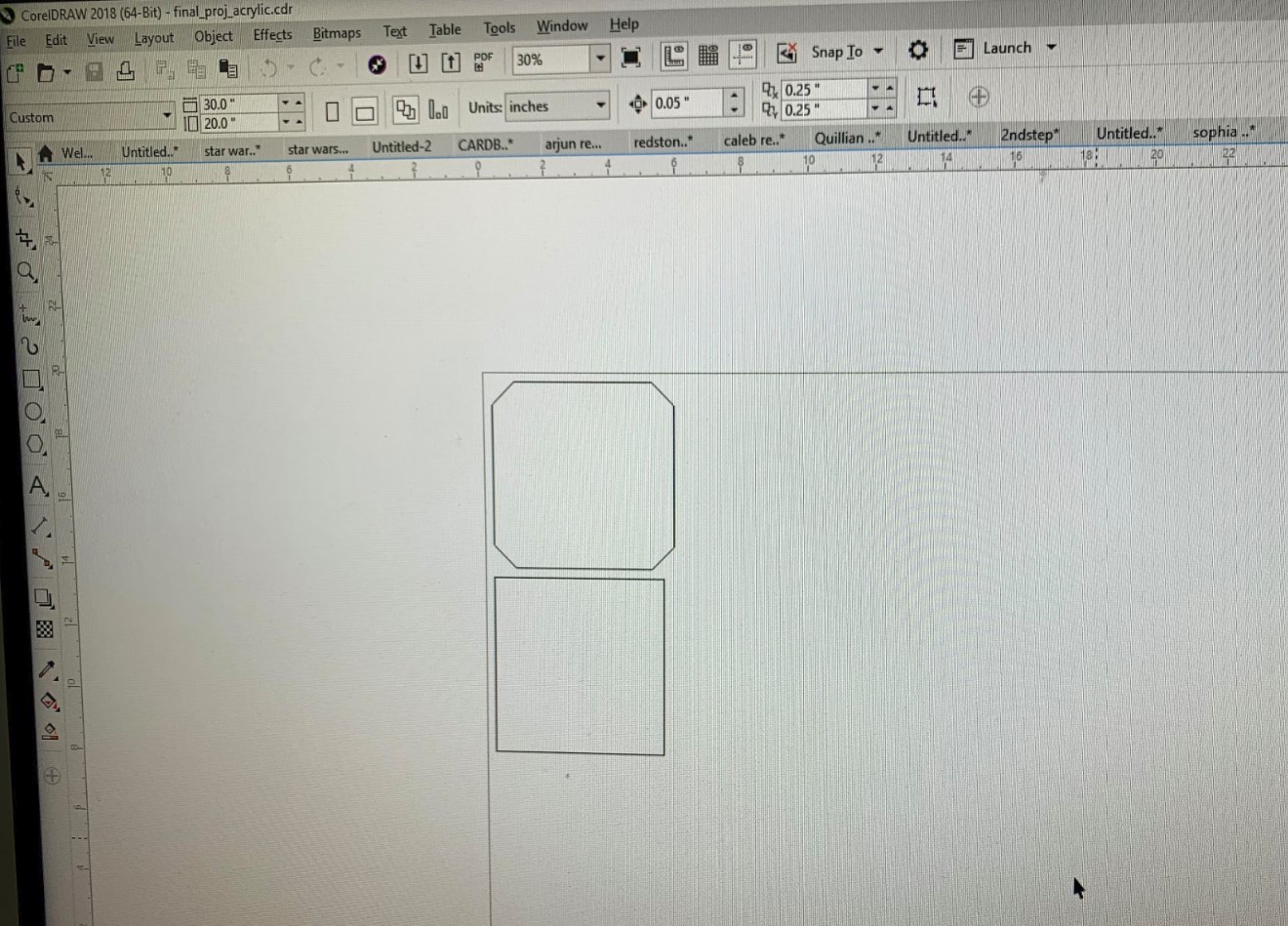
For my laser cut part in this project, I ended up using 1/8th inch acrylic to cut out two cover sheets for the two boxes in my project.
To make the files, I used CorelDRAW.
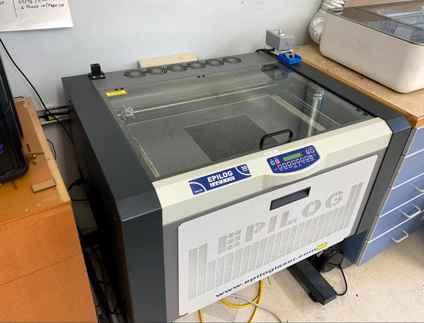
Then, I used our 30 watt CO2 laser to cut out the pieces. I’ve doccumented all about how to use the lasercutter here.
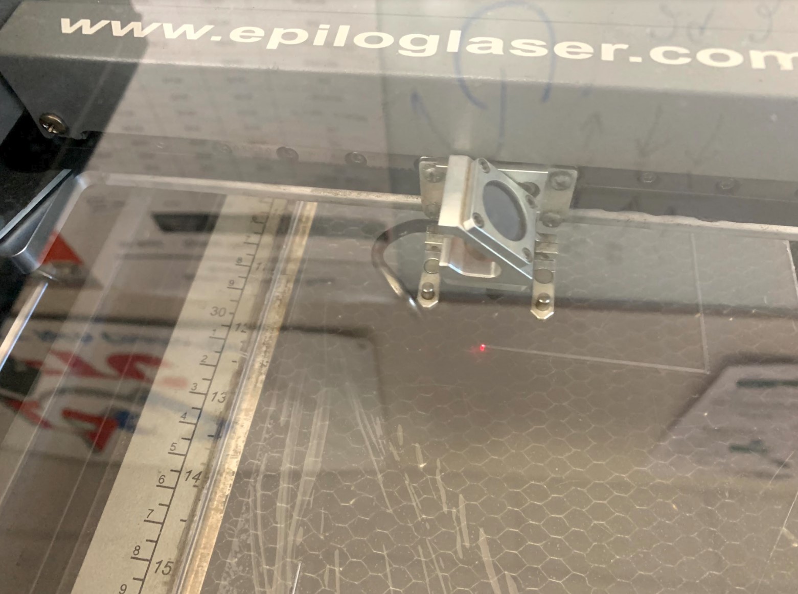
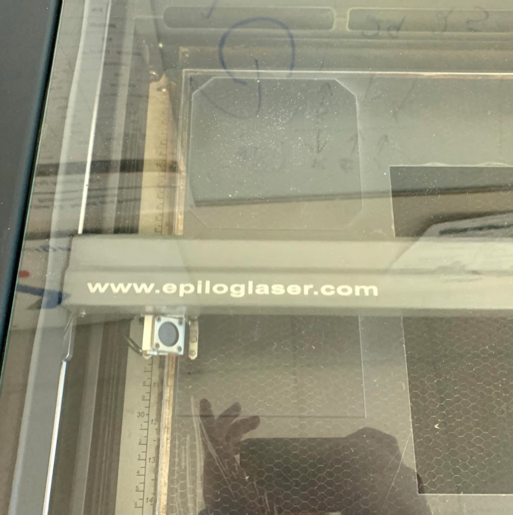
Once the cuts finished up, I attached them to the boxes.
Chosen Liscence
The license that I have chosen for my project is the Creative-Commons Attribution Noncommercial Share-Alike liscense. This means that people can use my work, but they have to credit me fully, they cant use my work to make money, and they have to licence any work they do off of mine under the exact same license.
Final Result
After all of that work, I was very happy with the final result. It looks a little confusing, especially underneath with all of the wires, but with some cable management it all ended up working out fine. It all works very well, and I am powering it from a single 5V 1A power brick with about 100 mA’s to spare.
This is my Presentation slide, and this is my presentation video.
Here are all of my files from my final project.