Exercise 07. Electronics Design
Situation
After the lesson about Electronics Design, on Wednesday 01 March, the assignment for this week was to:
			INDIVIDUAL ASSIGNMENT:
					_ redraw the echo hello-world board.
						+ add (at least) a button and LED (with current-limiting resistor).
					_ check the design rules, make it, and test it.
					_ extra credit: simulate its operation.
					_ extra credit: render it. (3D)

			GROUP ASSIGNMENT:
					_ use the test equipment in your lab to observe the operation of a micro-controller circuit board,
					use the circuit made in the individual assignment
PREVIOUS CONSIDERATIONS
Electronics concepts
Circuit design is the elaborate process to make an electronic circuit to satisfy a requirement.
Components:
_ Resistor: Limits the flow of the electrons through a circuit. The resistance is measured in ohms Ω. And an important aspect that we have to look at is the tolerance: how accurate it is. Current(I) = Voltage (V)/Resistor (R)
_ Capacitors: They store energy in an electric field and they can control voltage spikes (they “clean” circuits “noise”). They can be polarized and un-polarized. Capacity =Charge (Q)/Voltage (V)
_ Inductor: stores energy also but in a magnetic field.
_ Wire: allows the communication between programmer and the board.
_ Switch: this component allows you to control whether an electric circuit is opened or closed. They are very important for user interaction.
_ Resonator: Provide a clock signal to the circuit, it gives work frequency to the micro-controller.
_ Diodes: their main function is to control the direction of the current flow. They are directional components.
_ Transistors: A transistor is a semiconductor component that can either amplify or switch electronic signals and electrical power. A voltage or current applied to one pair of the transistor's terminals controls the current through another pair of terminals.
_ Regulator: It has a capacitor after. It establishes the voltage that you will have after it. If you have a higher voltage, 5V for example, you can regulate what it goes out, 3.3V for example.
_ Micro-controller: Brain of the PCB, each pin could have different functionalities, which would be defined later with Fuses.
INDIVIDUAL ASSIGNMENT
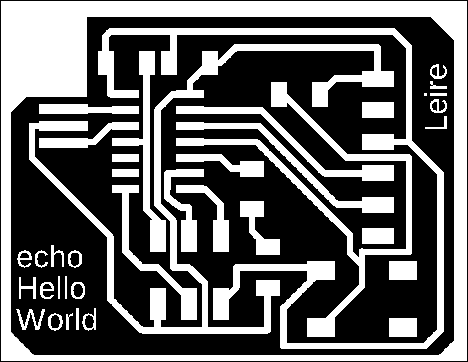
REDRAW THE ECHO HELLO-WORLD BOARD
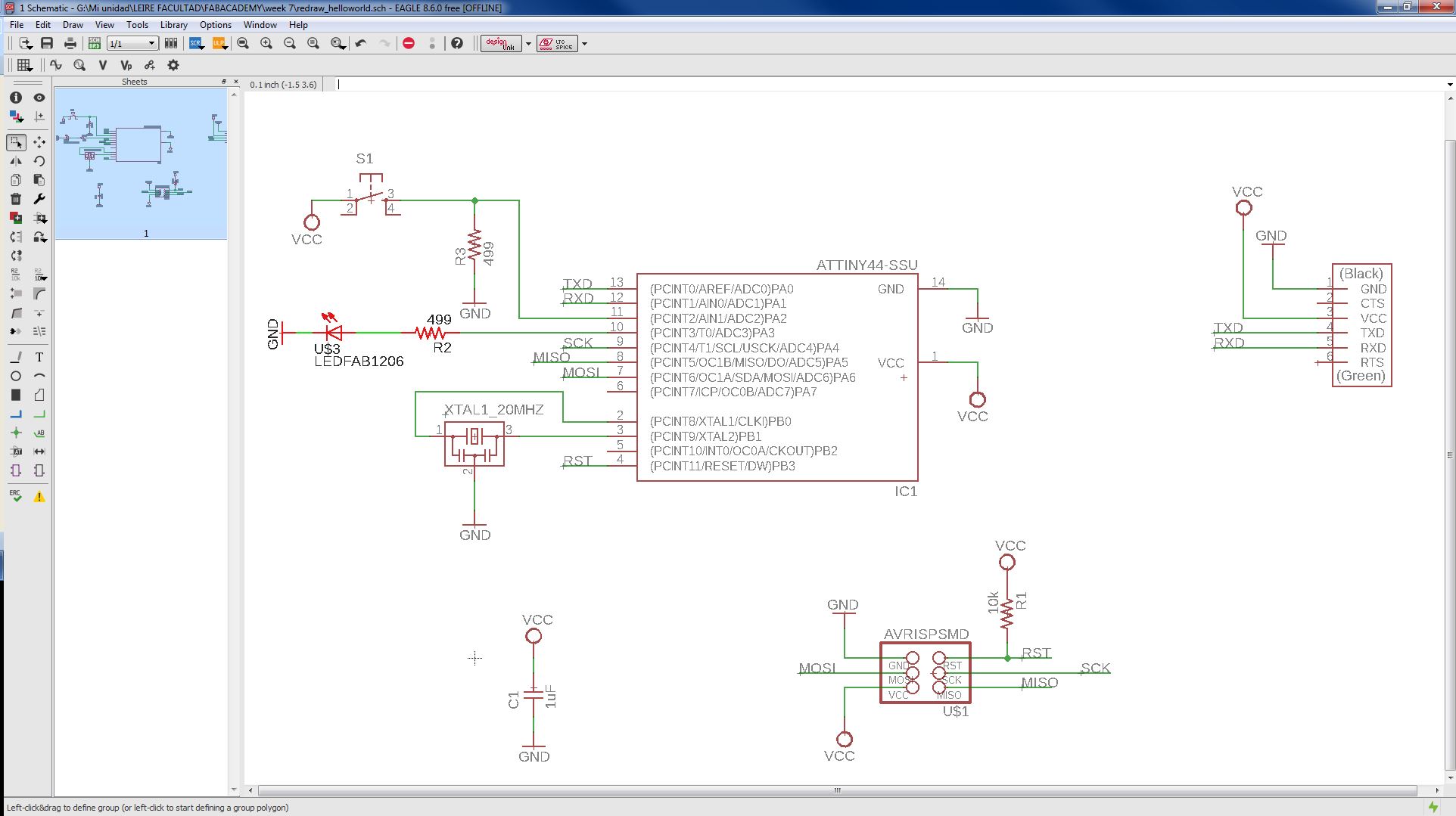
For this action, first of all, I had to take the Echo Hello-world board from the link here : board image, soldered components and board, traces image and interior image.
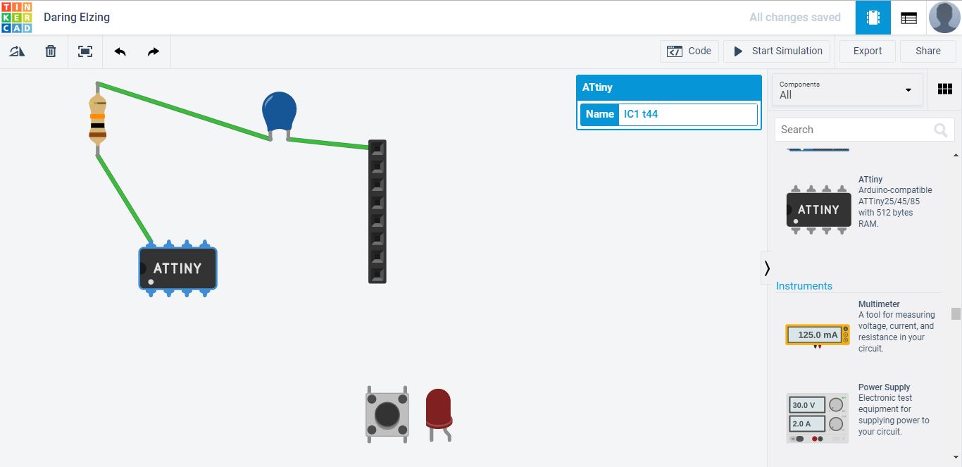
We were asked to redraw it, adding a button and a led, and we could use any software that we liked to accomplish this. I know something about Tinkercad Circuits due to Arduino, I have played with it years ago and we used to do here the simulations before mounting physical circuits. But, as Neil said on Wednesday, it is not for complexity and it is not parametric, it is fun way to the first time to play with circuits but it is very limited. I tried at a time to redraw here the echo Hello-world board but it hasn’t got all the components:
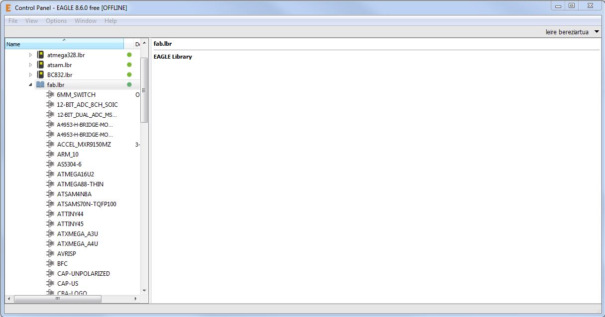
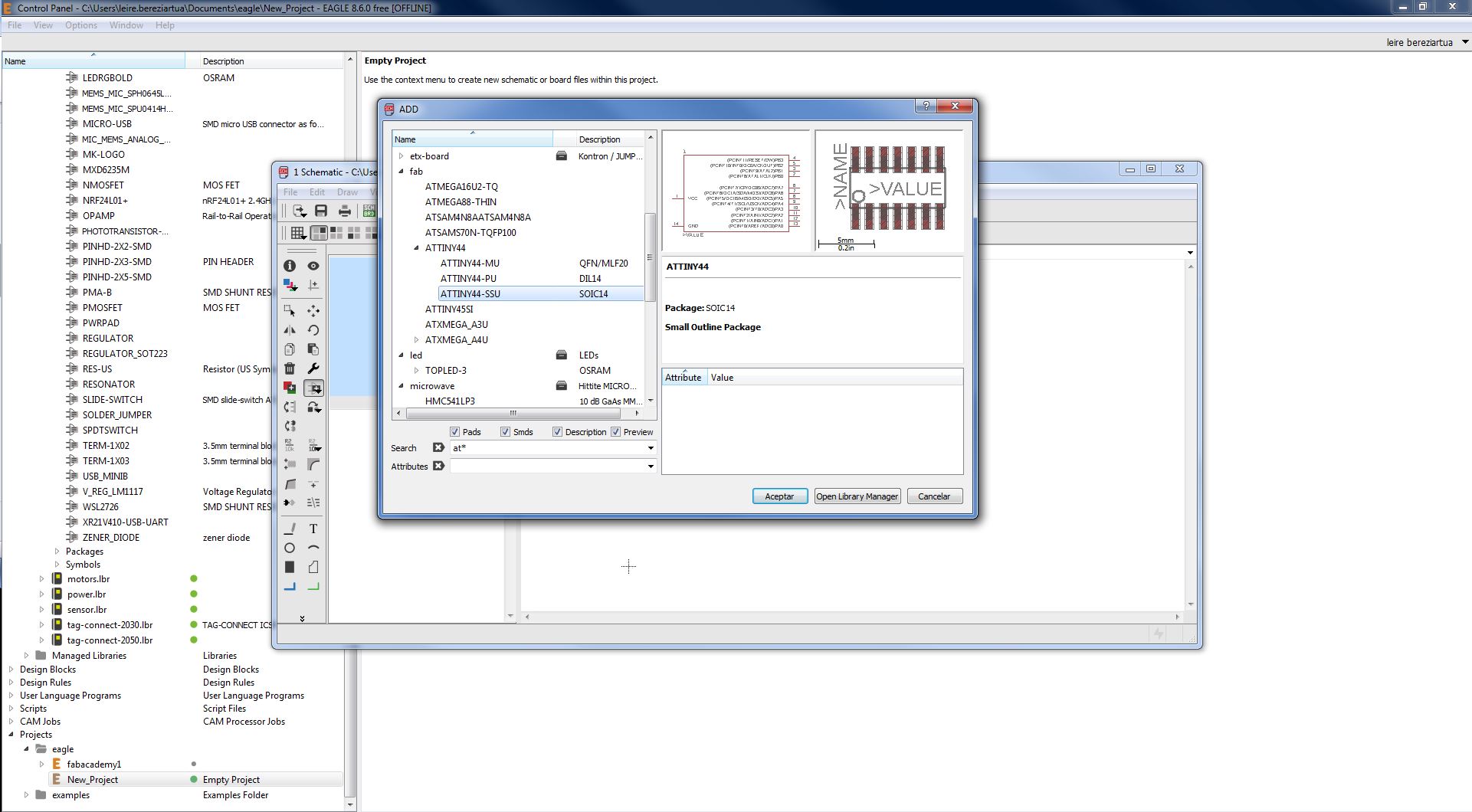
So finally I chose to use the EAGLE PCB Design Software which was highly recommended and easy to use. I downloaded and installed it in my computer.
The first step in this software is to lay out a schematic for how the circuit will operate, which involves knowing which components you will be using. I was able to import the fab.lbr which is a library containing all of the components that would be necessary for this assignment and made the selection process much easier.
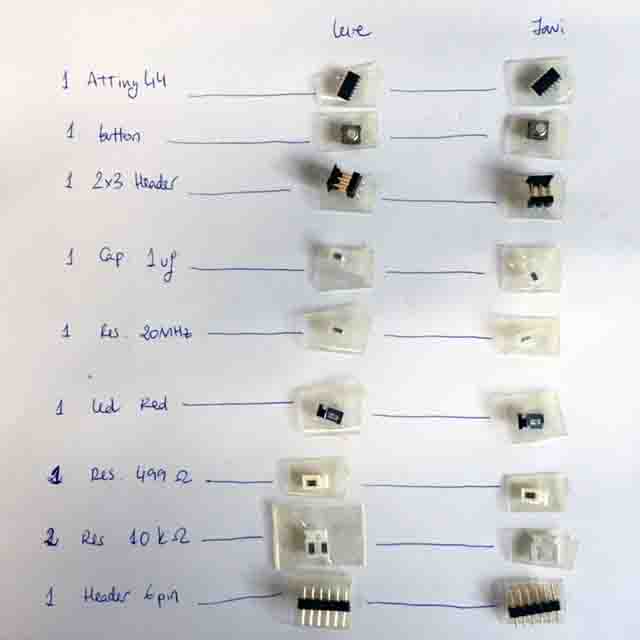
These are the components that I have used:
- ATTiny44-SSU, micro-controller
- AVRISPSMD, 2x3 header
- CAP UNPOLARIZEDFAB, 1uf capacitor
- RESONATOR, 20MHz crystal
- LEDFAB1206, one green for button
- RES-US1206FAB, resistors: (2) 499 ohm, (2) 10k ohm/p>
- FTDI-SMD-HEADER, 6-pin header
- SWITCH-6MM, button
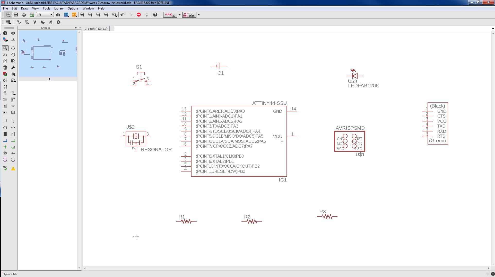
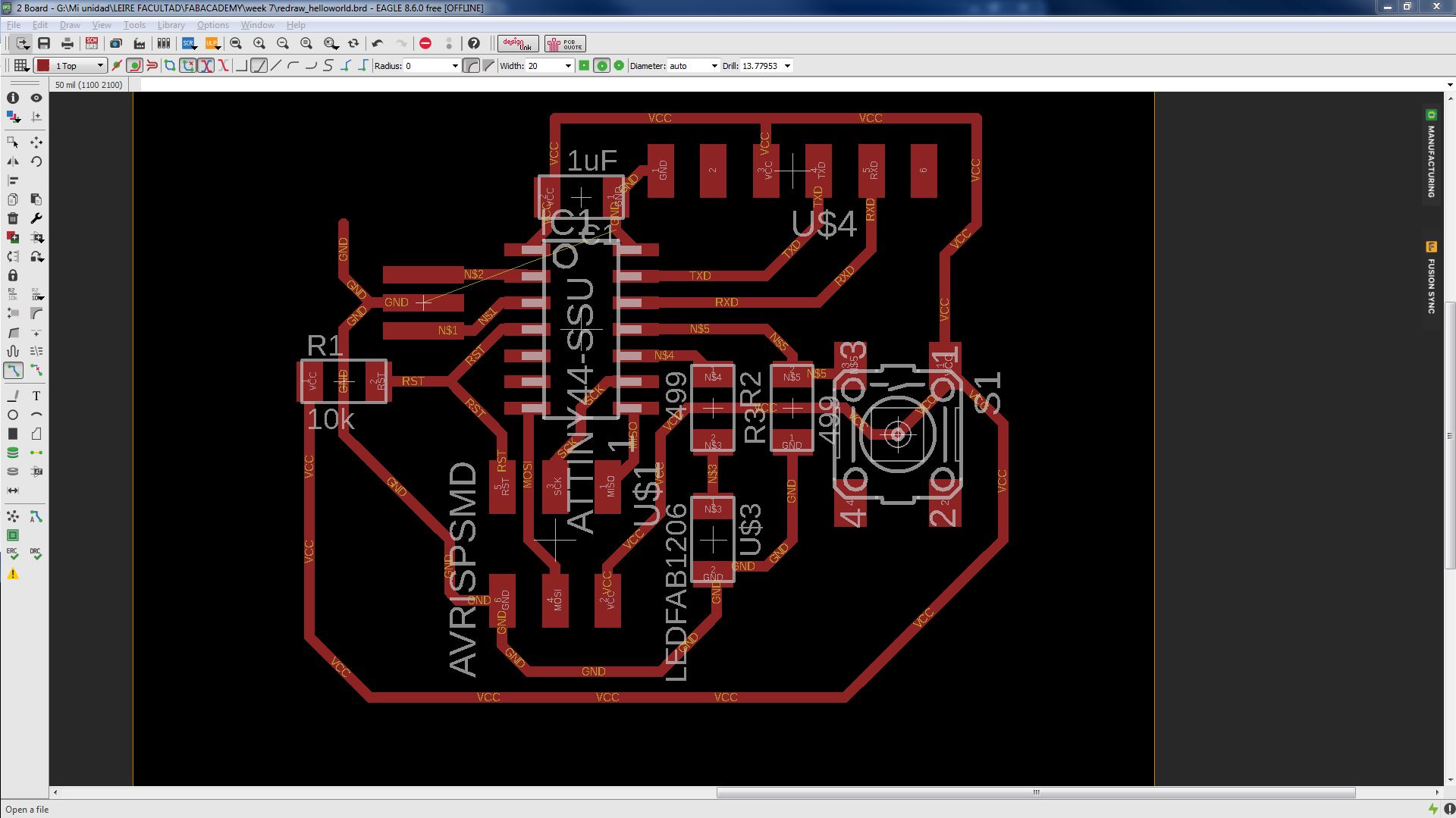
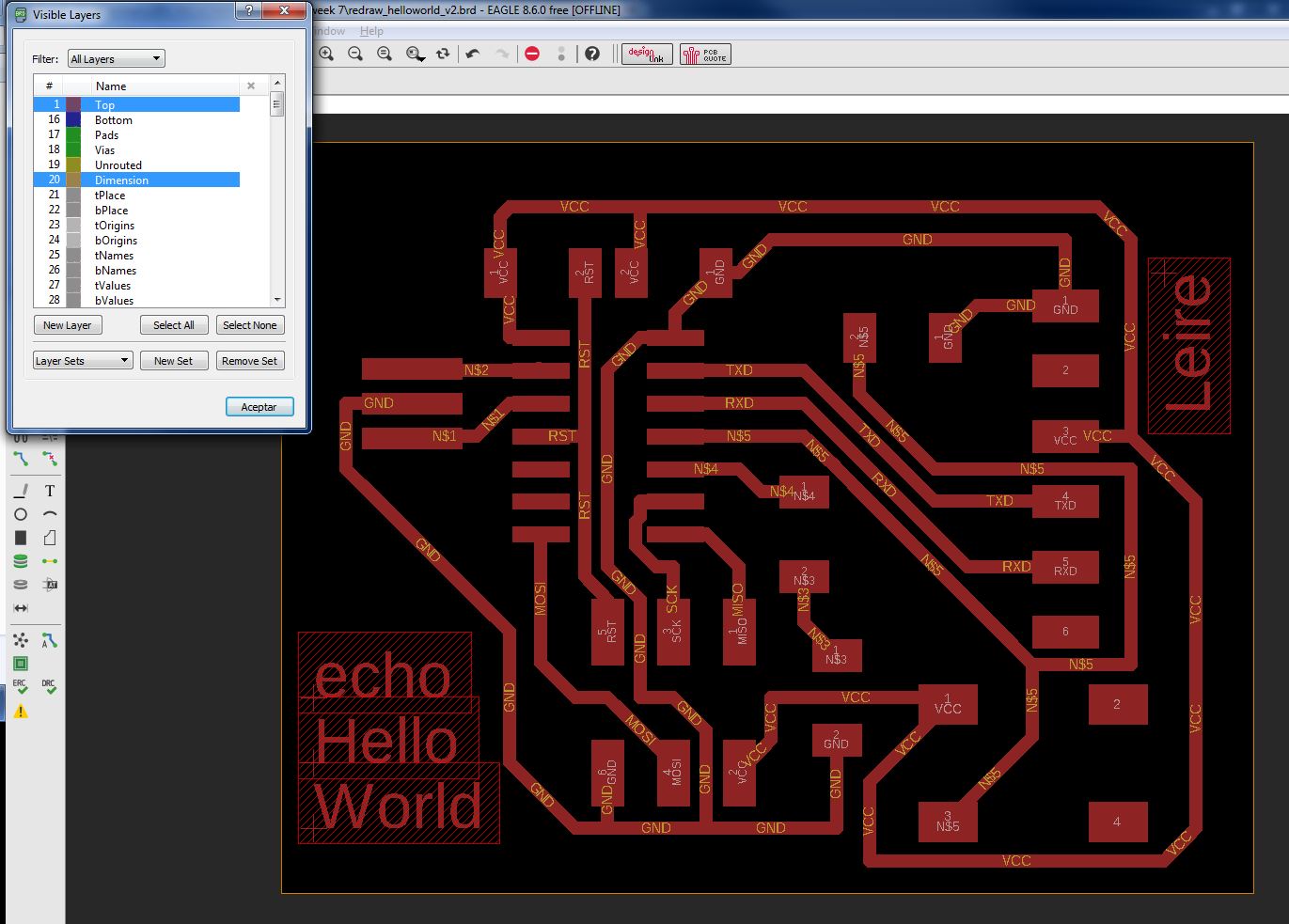
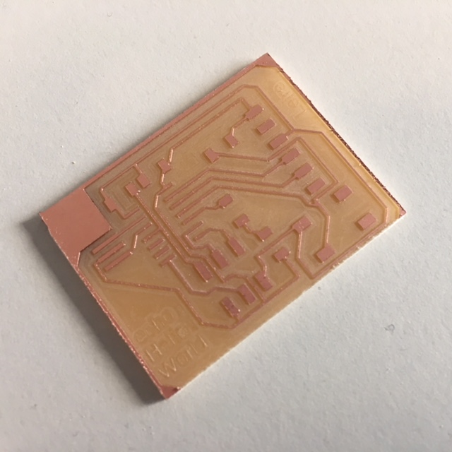
After laying out the components and creating "nets" between them, you can switch to board view where you position the elements as they will end up on the board and generate routes between them which will become the traces.
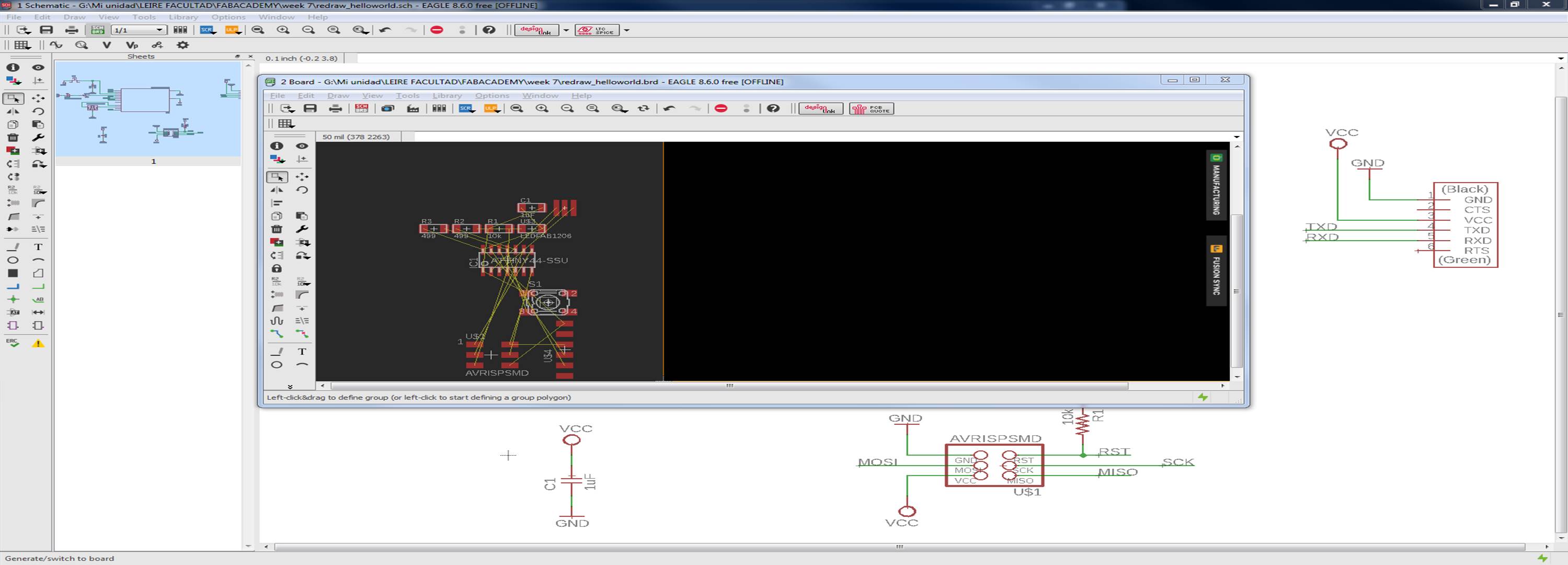
I have made two tries before obtaining a well-connected PCB. The routing step is slightly challenging as you do not want traces to cross over each other, but if viewed as a puzzle can be enjoyable. In the second round I had have to move all components!
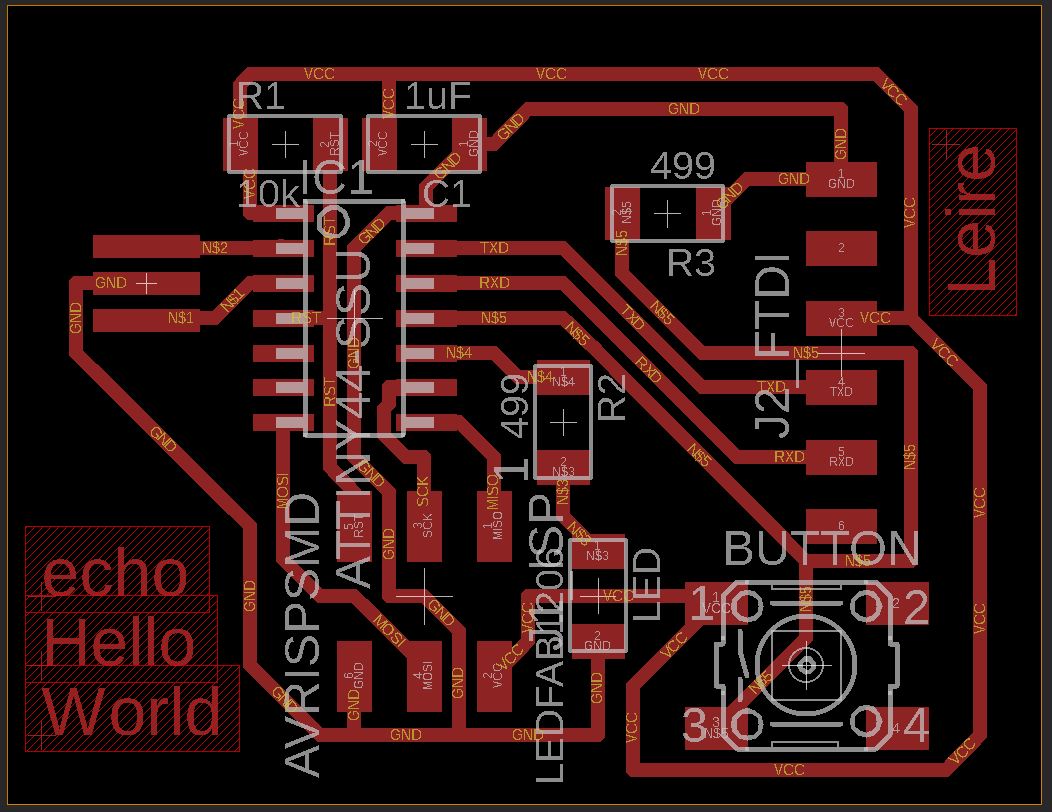
After the board layout looked good, I exported the traces and outline in the same .png file to then modify some aspects on Photoshop (reduce milling area, for example) and then go to mill on the Roland with a .bmp file.
First time I have imported it to Dr.Engrave (I first made a proof using Fab-modules, but it wasn't the option to choose Roland MDX-40A machine, and then, when it was calculating, it has been blocked, so I desisted), I realize that there were 2 points in which the milling process will be problematic, so I have opened Eagle again, and I change some routes distances to improve PCB design.
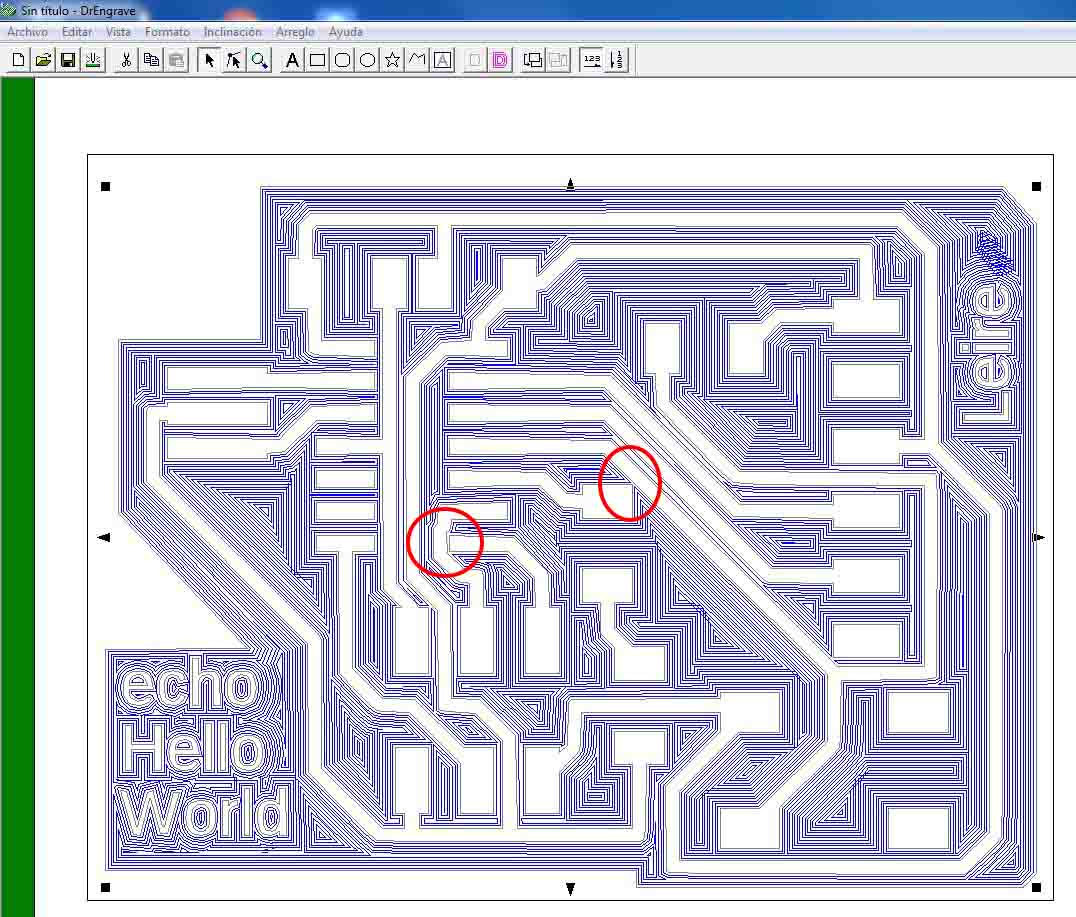
So I opened again it in Eagle and I move some traces to get them more separate each other.
Then, I made process again and when I saw it was right, I prepared Roland machine to mill it as I have done in exercise 05 .
You can find my Eagle files here and Dr.Engrave file here.
MAKE IT
In this case I have made a deeper analysis about the Engraver V tool we are using, to be sure of the width of the tool when we are going Z down 0.15 mm to engrave process, since, although the specifications of the tool should tell that was 10º angle, in reality it is not.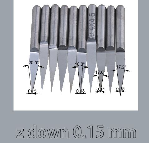
*We have to make more tests with this Engraver tool, it has done too thin traces this time :S For this kind of work it is fine, but it would be a big problem if we need to connect motors or heavier components there, they could be burned and not working.
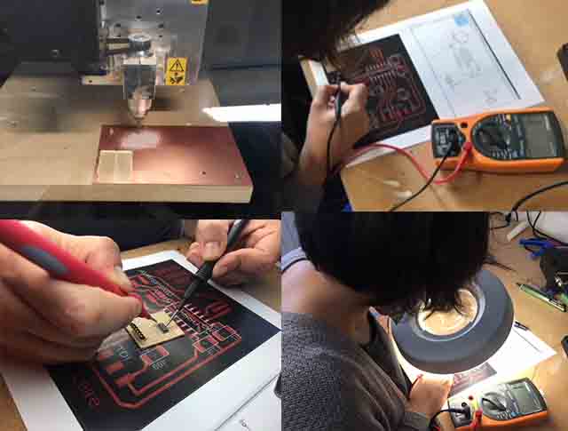
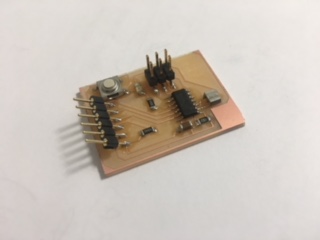
Once I had my milled PCB, I went to work stuffing it with the components, starting with the FTDI header. As Neil said, it is important to have this component near the edge of the circuit and I didn't remembre it, so I had it in a delicate place, on top of some traces.
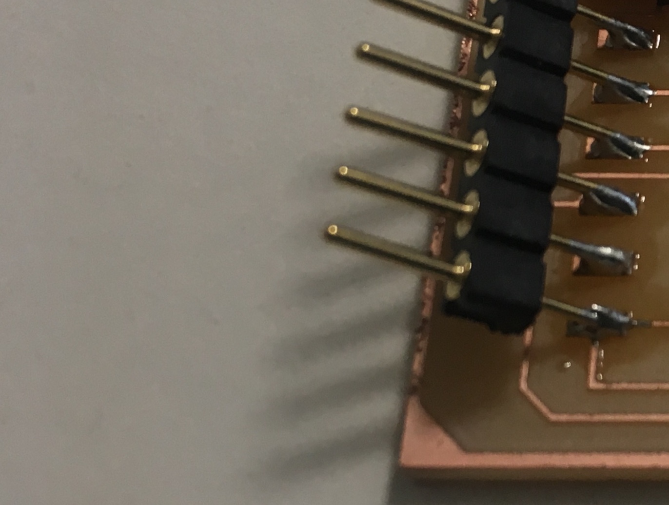
When I saw it was possible, and did it, I used the magnifying glass while soldering the components on this board, which I found to be very useful for the ATTiny 44 pins, which are so small.
I soldered first ATtiny 44 micro-controller, which is in the center part of the PCB, and then the other components around.
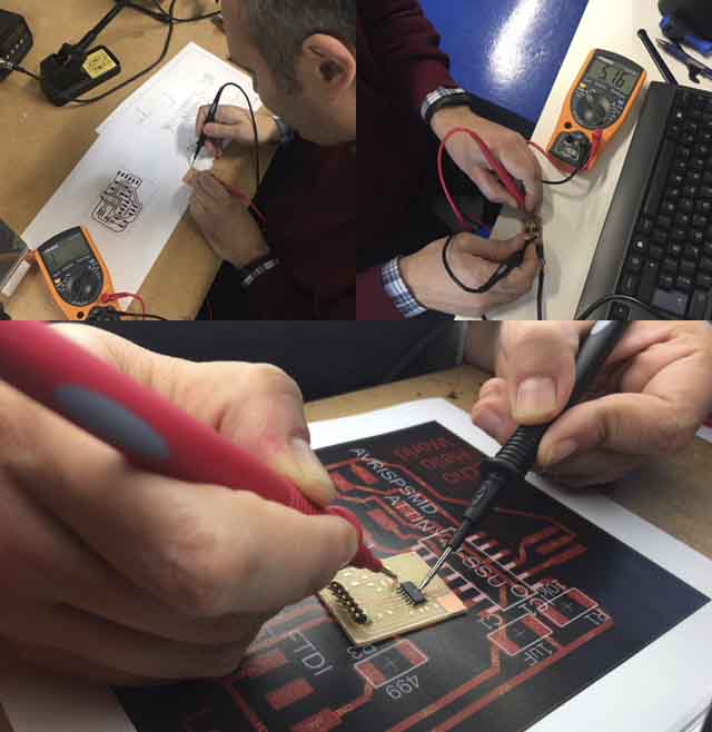
While I was soldering components, I test every pin and traces connection using a digital multimeter, to confirm that the traces were good and the board was receiving power.
TEST IT
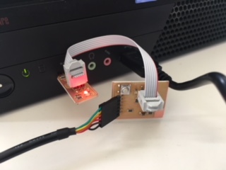
To test it physically we need to program it first. So, downloading from the site these two files:hello.ftdi.44.echo.c and hello.ftdi.44.echo.c.make, and following exercise 05 programming process, we did it:
i_ Connect with each other echo Hello-World PCB and USBTiny programmer, and then both to computer USB ports:
ii_ change name to file hello.ftdi.44.echo.c.make >> to Makefile
iii_ cmd.exe and execute: "make", "make program.usbtiny" and "make program-usbtiny-fuses"
The fact is that: We have added a led with a button, so what are they going to do? We have to program it.
1_Programming it with C: (Javi has helped me due to my low knowledge in this area)
i_ We have made a research and downloaded files needed to program a ATtiny44 micro-controller using cmd.exe.
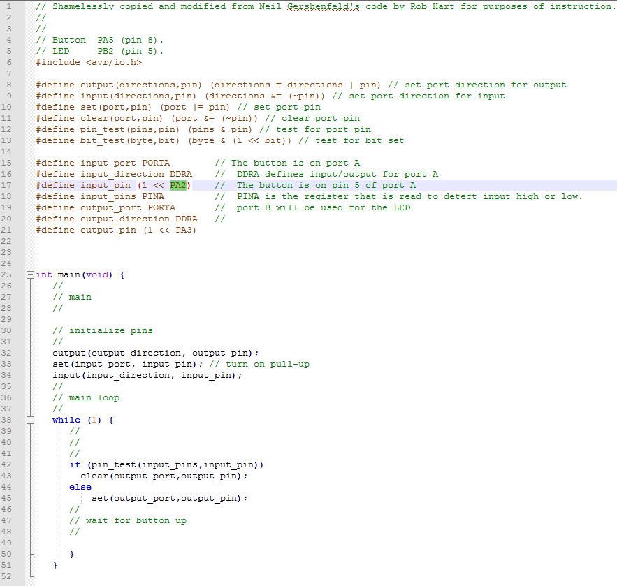
ii_ We took button_44_c.c file, and understanding which pin was output (Led) and input (Button), we changed this two variables with Notepad++.
iii_ We follow exercise 05 programming process, and it went OK!
The key in this option for programming is that it is complex and it needs knowledge about micro-processors inside architecture (cells, 0 and 1 positioning, OR and AND functions, DDRA, DINA, ecc.) and it is not easy to everybody :S
2_Programming it with ARDUINO: (easier way)
i_ Download Arduino software from the site.
ii_ In Internet we can find a lot of tutorials like this. In this web-page we can find a link to "install" ATtiny micro-controllers in Arduino libraries in Preferences.
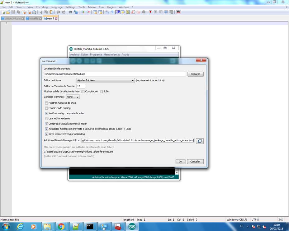
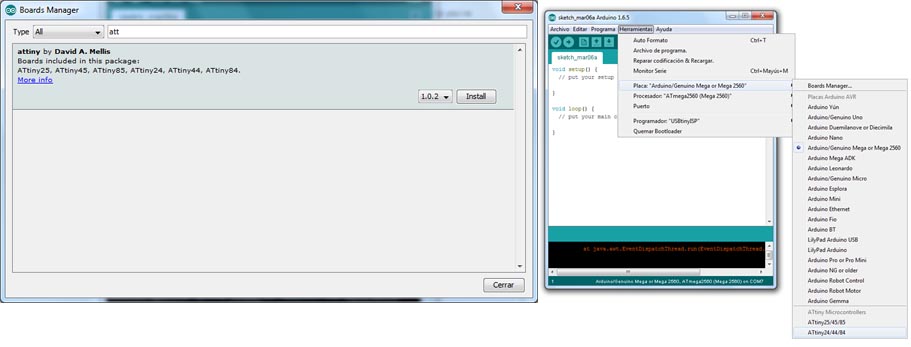
iii_ Select, in Boards Manager attiny and install it. Then, in Tools (Herramientas) select ATtiny44 as processor and USBtinyIPS as programmer.
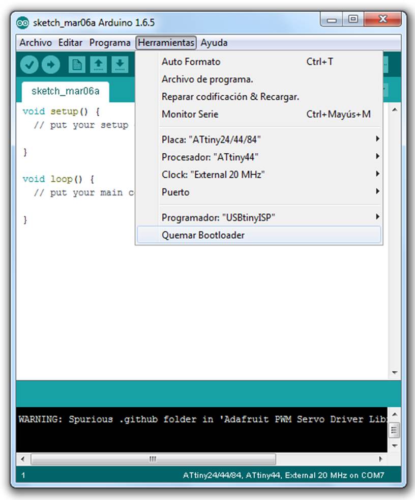
iv_ Burn Bootloader ("Quemar Bootloader") to say to USBtinyISP and PCB to be programmed with Arduino.
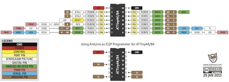
v_ See ATtiny scheme below to know each connection pin number in Arduino language. My scheme says that my INPUT (Button) is pin 2 and OUTPUT (Led) is pin 3.
vi_ Write the program taking in account these pins:
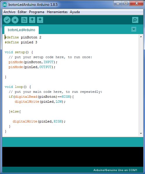
!! First time I made a mistake, I have write to have Led switched on everytime, and switch off it when Button was pushed, but I change it and it works well!
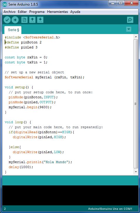
You can find my Arduino two programs here.
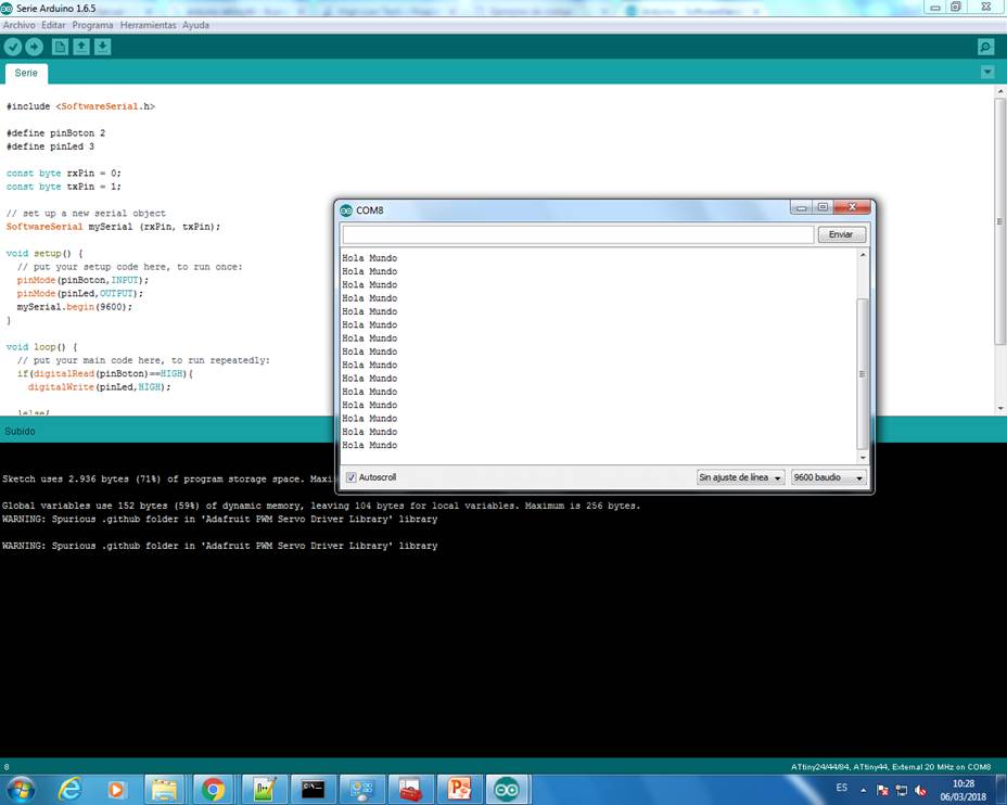
vii_ Test it with Arduinos :
It says "Hola mundo" (Hello world) and when I push Button in PCB the Led switches on, yeah!
*Future plans: download FabAcademy Arduino libraries.
RENDER ECHO HELLO-WORLD PCB
I have installed Fusion 360, also from Autodesk. It is free for educational related users like students or teachers.
And I found a tutorial to link Eagle files with Fusion files, so I have been making proofs with it.
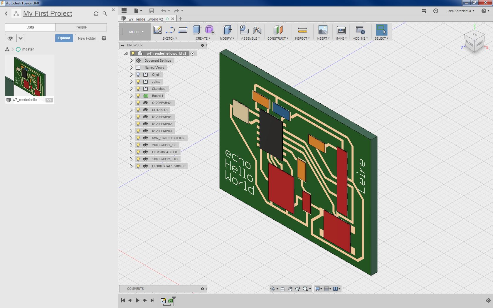
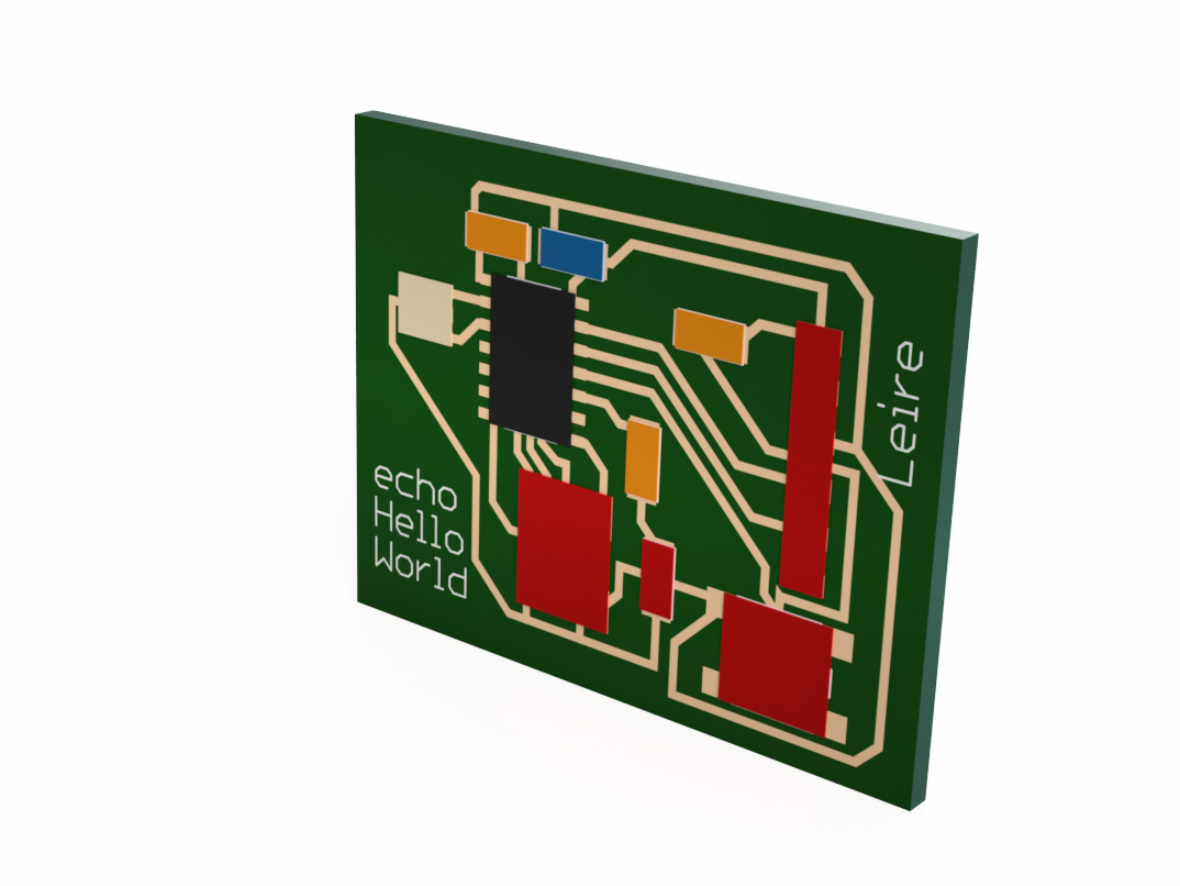
I also proof in BRD Viewer: it is a free on-line tool for rendering Eagle PCBs. It is easy to use, and results are very realistic:
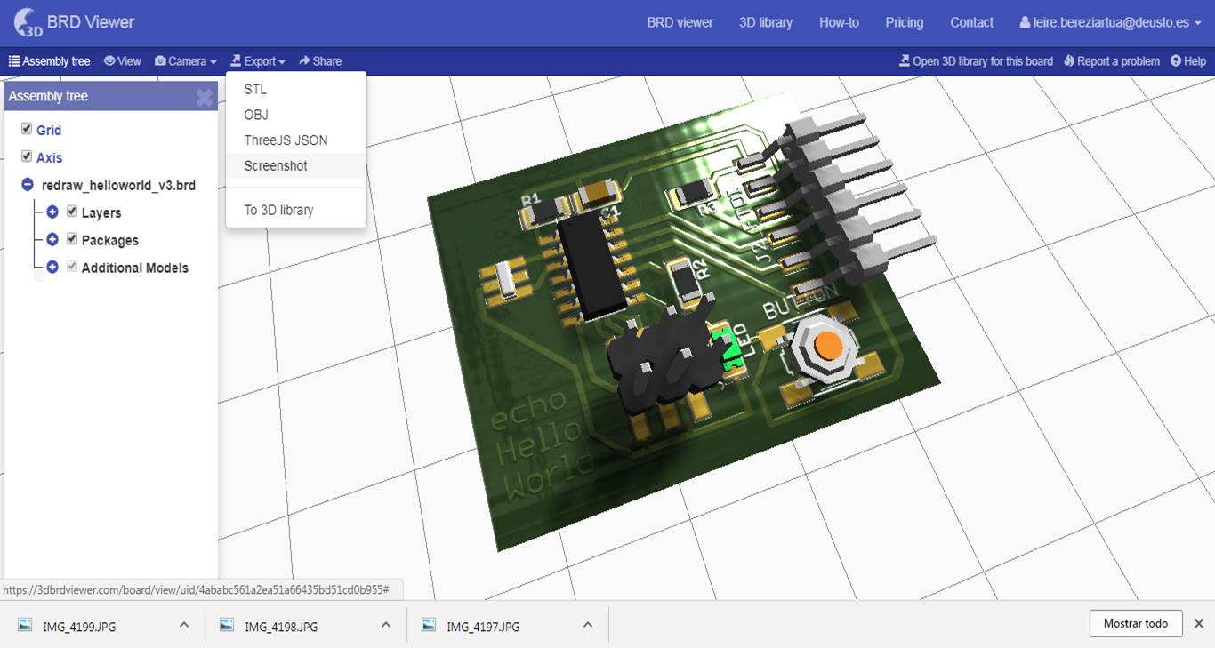
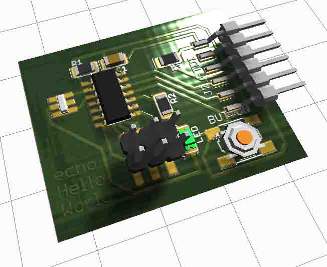
The unique problem is that we have used Fab-Components and it hasn't recognize them, because of its libraries, so I have had to link them manually using generic components.
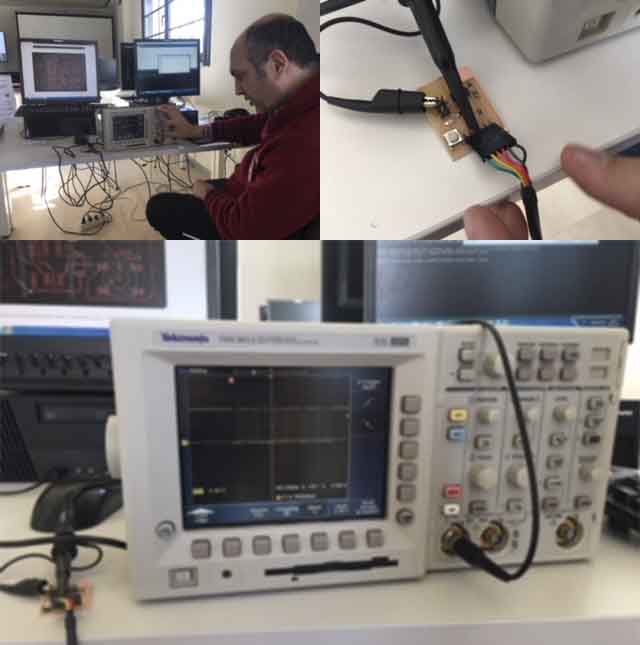
GROUP ASSIGNMENT
Once Javi Vicente and me have our PCB soldered, we test equipment in our lab to observe the operation of a micro-controller circuit board.
First of all we soldered the FTDI-SMD-HEADER (6-pin header), as I comment up in the individual assignment, and we connect 5V to it. With the digital multimeter we verified if each connector first of soldering the other components, to avoid burning them later, if it is not working well. Then, we use it to verify every connection pins and traces too, while we were soldering the other components. A digital multimeter (DMM) is a test tool used to measure two or more electrical values—principally voltage (volts), current (amps) and resistance (ohms). It is a standard diagnostic tool for technicians in the electrical/electronic industries.
Then, when we have PCB programmed and connected to the computer, we use the oscilloscope. An oscilloscope is a type of electronic test instrument that allows observation of varying signal voltages, usually as a two-dimensional plot of one or more signals as a function of time. Other signals (such as sound or vibration) can be converted to voltages and displayed too.
With this tool we could see the signal spectrum of the PCB "saying Hello world":
DOWNLOADS
_ ECHO HELLO-WORLD redraw BMP file
_ Files needed to program a ATtiny44 micro-controller using cmd.exe