Exercise 05. Electronics Production
Situation
After the lesson about PCB fabrication, materials and components, on Wednesday 14 February, the assignment for this week was to:
			GROUP ASSIGNMENT:
				_ characterize the specifications of our PCB production process.
			INDIVIDUAL ASSIGNMENT:
				_ make an in-circuit programmer by milling the PCB.
GROUP ASSIGNMENT
My FabAcademy mate, Javi Vicente, and me have to use the ROLAND MDX-40A machine to mill our PCB.
The MDX-40A High Precision CNC Milling Machine produces affordable and highly accurate prototypes from a wide variety of non-proprietary materials with greater precision and excellent surface finish.
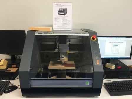
In this machine: X, Y, and Z operation strokes are 305 (X) x 305 (Y) x 105 (Z) mm.
And the softwares we have used are: Dr.Engrave and V-Panel. They are Roland specific drivers, which allows us to control the files we are going to engrave and cut, and machines parameters. None the less, we want to make tries with FabModules to master the control of the machine using this platform.
Dr. Engrave is a user-friendly program to engrave plates. It supports variable data, so you can engrave the same design on a series of plates with variable text or numbers. You can also engrave the space on the inside of a selected vector or text. The software can also detect the outline of an image and convert it to lines.
VPanel is a program to operate the modeling machine on the computer screen. It has functions to output cutting data, perform maintenance, and make various corrections.
You can find the document we have followed to make our in-circuit programmers here. It is the ATtiny45 process Brian has used to build his FabTinyISP.
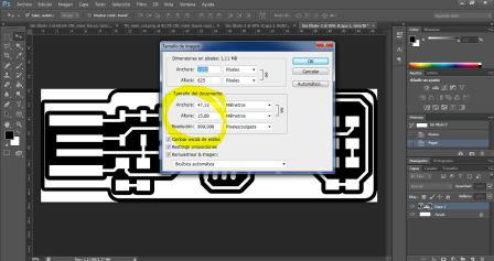
But, first of all, we needed to prepare the files from .png to .bmp, the file type Dr.Engrave uses to prepare the milling.
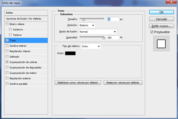
We opened Adobe Photoshop and we mesh Traces and Outline CutOut .png files maintaining the 1000dpi property. Then, the work was to obtain the perfect traces width and to optimize the engrave action of the machine, by using offsets, not to take time removing cupper “for nothing” in some sides.
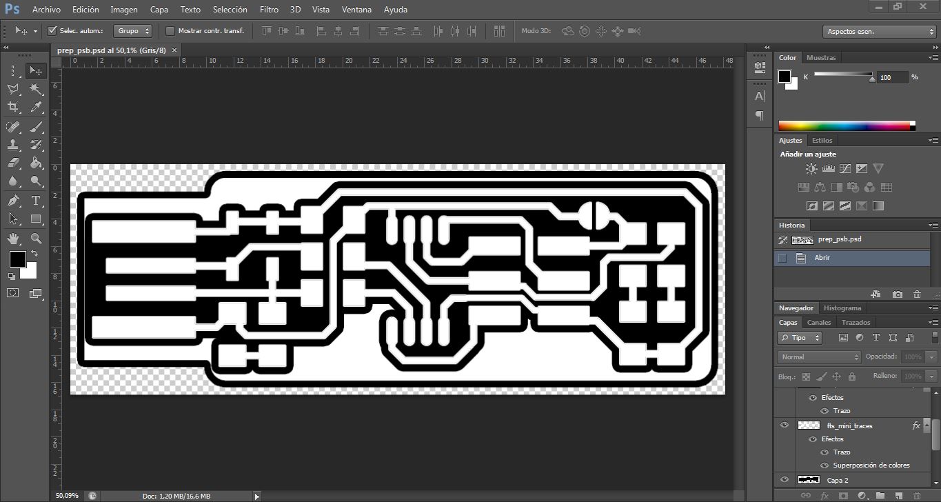
It is important too, having a 1000dpi file, to know the exact dimensions the PCB has to have:
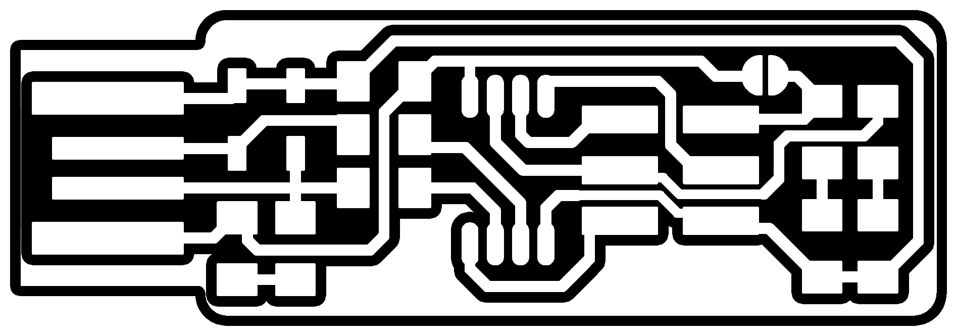
Once we have the .bmp file, we Import it in Dr.Engraver. To see the .bmp file click here.
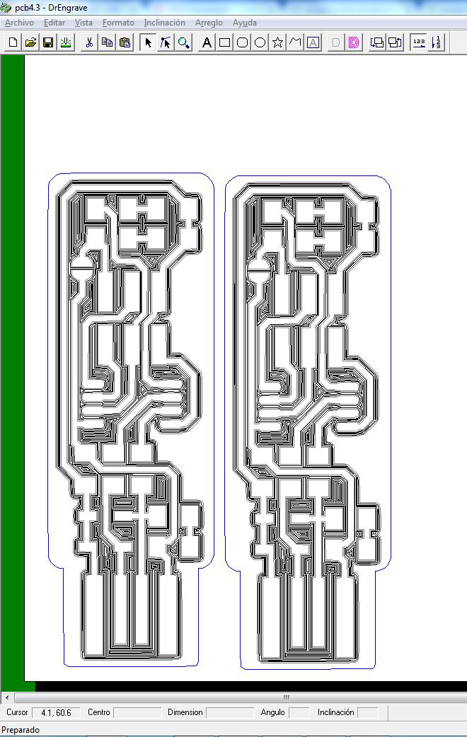
The work to do is:
_ Re-mesure included .bmp image size and re-sized it (47,12x15,88 mm) based on the 1000 dpi.
_ Separate all lines, and unify together the lines that compose traces. This action will simplify the selection of lines to each action: Engrave and Cut.
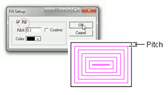
_ Select Traces line-group and Fill Setup with a Pitch of 0.1 (it depends always on the tool we are using, explained below), without “Contour”. The tool path is created on the inner side of the object.
Then we have to send them to mill.
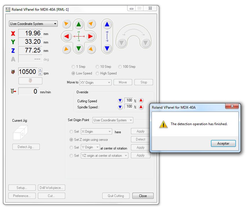
For this action, we have to prepare the machine: Material and axis origins (V-Panel).
We can use two materials in the PCB milling process:
• FR4: epoxy glass. We won't use it as is dangerous for health and also because the tool will wear out fast
• FR1: not as good at high temperatures but it machines beautifully.
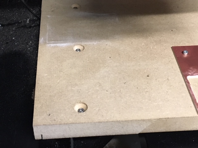
We chose FR1, and we attach it to the machine using the Sacrifice layer: The actual Roland plate is swapped for the DM sacrifice layer you see in the machine because of functional reasons (it is cheaper to swap a sacrifice layer than the actual Roland plate). In our case it is a piece of DM with threaded holes, it has underneath a simple nut and that is what helps us to screw down the PCB to mill, to be able to join the material on it.
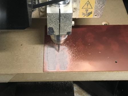
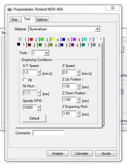
ENGRAVE ACTION
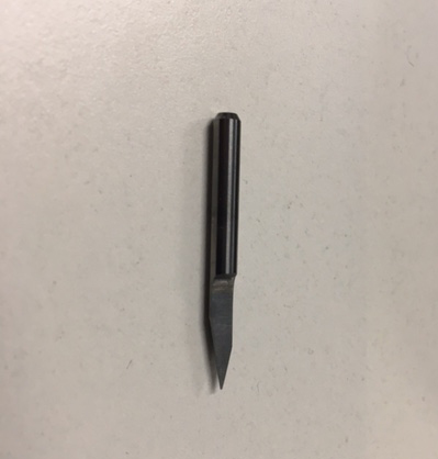
The tool we chose for engrave milling is 0.1mm Carbide Engraving Bits CNC Router Tool for PCB Board .
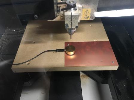
We put it in the machine head, carefully, due to its fragility and, using V-Panel, we set X, Y and Z origins. For setting Z origin we have a sensor you can see in the images below:
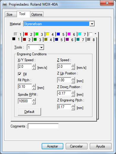
Back to Dr.Engrave we select “print” mode and in Properties we set up all the engrave parameters we need to make traces with the tool we are going to use. As we use Engraving Tool in V, good to engrave small and detailed items, we need to calculate how much the Z DOWN position had to be not to remove too much cupper, it would erase the Traces in that case and it is not good!
Parameters we used are:
_ Speed (X, Y, Z): 2 mm/s
_ Fill pitch: 0,1 mm
_ Spindle RPM: 10.500 rpm
_ Z UP Position: 1 mm
_ Z DOWN Position: -0,17 mm
_ Z engraving Pitch: 0,17 mm
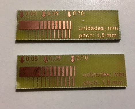
The reason of Z down position 0,17 is: we have done some tests (you can see it in the image below) for ensuring the depth that we must give to our tool to remove the copper layer properly. The sacrifice plate is not completely aligned with the surface of the machine (+-0,1mm), so we must ensure a depht for etching that removes the material well on the entire surface of our plate (in this case we have used FR4, with all the necessary security measures, to do these templates. After that we have used always FR1), although we know that the copper depth of this is 35 microns. After these tests we saw that we need 0'17mm Z down. :)
And we send to “print” the selection:
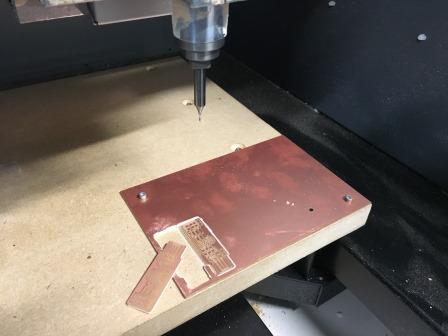
CUT ACTION
For doing the Outline Cutout we had to change the tool. In that case the tool we used has been 1 mm Straight End Mill, suitable for cutting flat items.
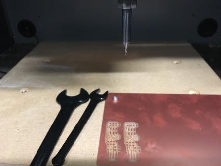
We have set again the Z origin, and after selecting the outline, the parameters we used for make the cutting action were:
_ Speed (X, Y): 1 mm/s
_ Z Speed: 0,5 mm/s
_ Fill pitch: NO
_ Spindle RPM: 10.500 rpm
_ Z UP Position: 1 mm
_ Z DOWN Position: -1,6 mm
_ Z engraving Pitch: 1,6 mm
And we send to “print” the selection:
All has gone fine in the first try so we are so happy!
INDIVIDUAL ASSIGNMENT
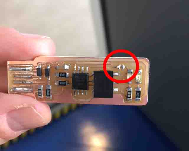
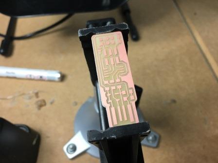
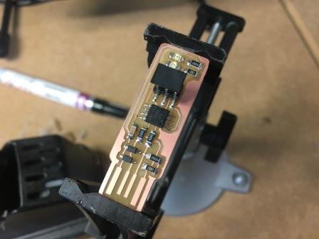
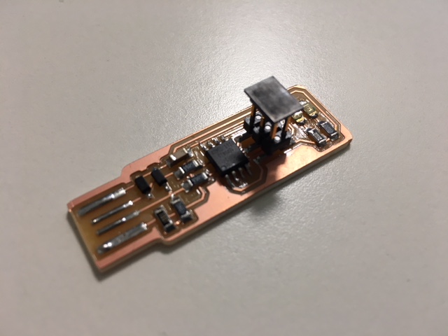
Once I had milled the board and I had washed it, this is the result of my PCB before being soldered:
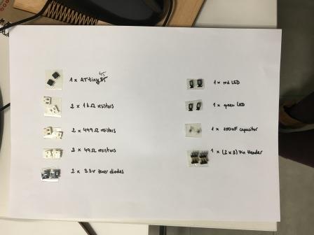
The components I used are:
1. ATtiny45small: Directional, it has a circle in the bottom left corner
2. Two 1kΩ resistors
3. Two 499Ω resistors
4. Two 49Ω resistors
5. Two 3.3v zener diodes, marked with a line on the cathode side.
6. One red and one green LED: they have a green line to know the cathode direction.
7. One 100nF capacitor
8. One 2x3 pin header
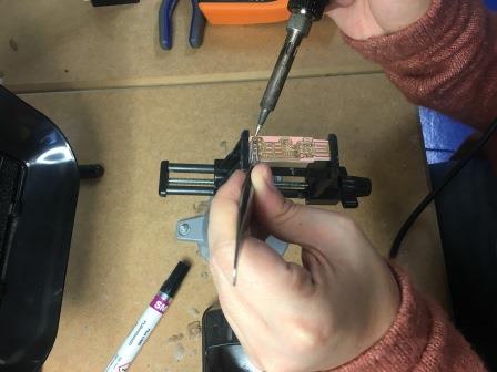
And it was almost the first time I was going to solder a PCB (I remember a little practice I did first year at the university :S) so I read about how to solder the components well:
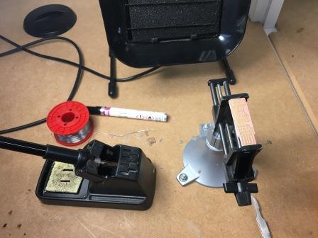
1. Wet the sponge for cleaning the tip of the heater.
2. Cut the a piece of solder from the roll to work better with it.
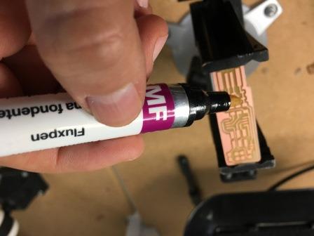
3. Put some flux on the board for transmitting better the heat and a better fixing.
4. Start from the bottom to the top and inside out.
5. Checking that there is continuity between the components.
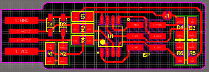
Scheme that I had to follow to place them:
The tutorial recommends starting with the most difficult parts, in this case the micro-controller, but I preferred to start soldering from one side to the other.
The general process to solder is:
• You smoothly put a bit of the solder
• You wait to the right temperature (10s aprox)
• The solder will flow up and down
• You take out the solder
One advice I read and it helps me has been: to place some solder material in one of the two connectors of each component location, before beginning to solder the components one by one.
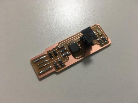
Then I began from leds and their resistors, and I continue one by one with all components, turning around the board to have the best position.
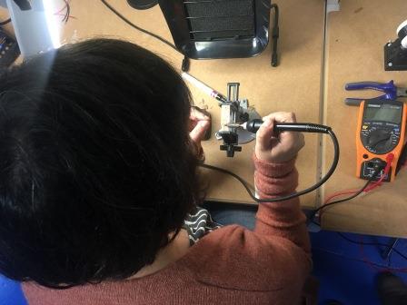
While I was soldering the components I checked the continuity looking at what connections they had in the red scheme to avoid short-circuits.
The PCB ends up just slightly thin to work well in most ports, so I flow some solder onto the USB contacts on the board to build them up a little bit.
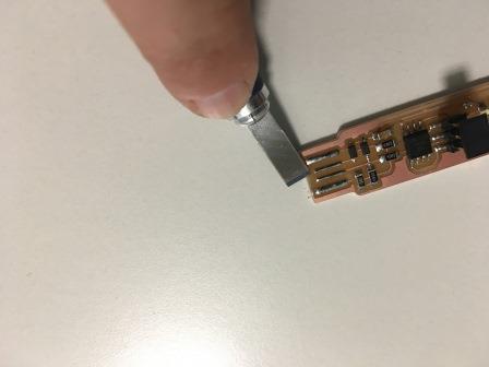
I realized that my PCB had a copper little line in front of the USB, so I remove the extra copper with a knife. Only the copper in front of the pads needs to be removed; the copper left on the sides is fine.
And woala! That is the result of my first PCB:
PROGRAMMING THE ISP
Steps to follow to program the PCB are:
1. To program the FabISP, you first need to install the necessary software for your operating system and download the firmware.
2. Then you edit the Makefile
3. Set the fuses / program the board
4. Verify that the board is working properly
5. Then you need to open up the jumpers to make it a programmer.
1. Install Necessary Software for AVR Programming:
I have Windows 7 Professional and I used this files for doing my computer able to program my PCB to be a ATtinyISP.
Proceed is:
_Install WinAVR-20100110.intall.exe: C compiler for Atmel micro-controllers.
_Copy make.exe: For being able to execute makefile and its actions to program our PCB.
_Install adafruit_drivers_2.0.0.0.exe: Drivers to recognize the ATtinyISP.
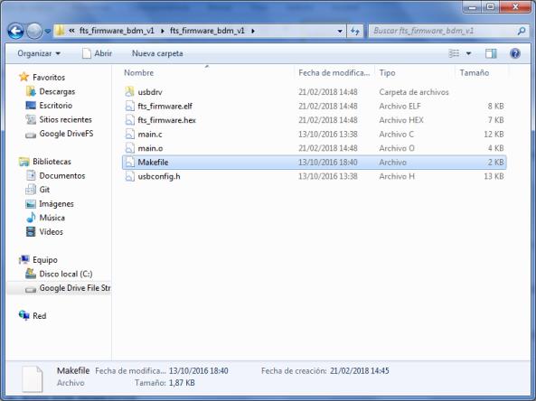
Then, we have to download the Firmware source code and decompress the folder with the files in our computer.
I will use my example >> the folder where I have decompressed the folder is G:\Mi unidad\LEIRE FACULTAD\FABACADEMY\week 5\para programador en windows\fts_firmware_bdm_v1\fts_firmware_bdm_v1.
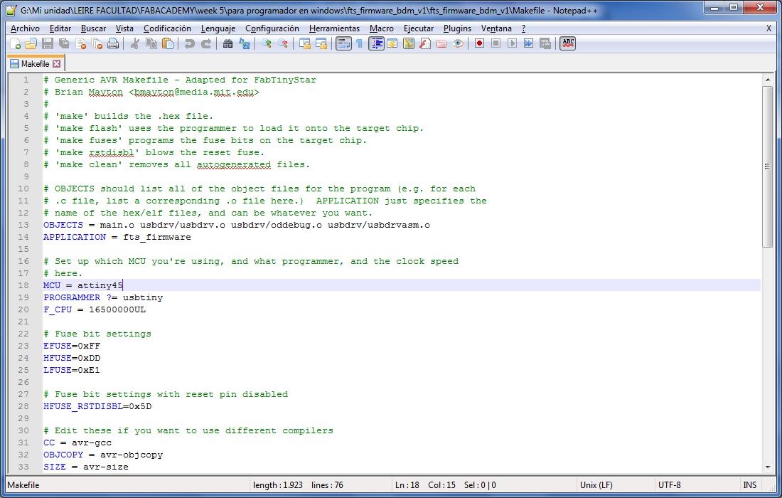
2. Edit the Makefile:
Edit makefile file with Notepad++.
In my case, I will not change anything in the code because the programmer I am going to use is the usbtiny we have in our FabLab. It is our instructors, Szilard Kados, UsbTiny. But be careful and read all specifications and see if you need to set up the MCU you're using, and what programmer are you going to use.
3. Set the fuses / program the board:
Connect with a Ribbon cablethe pcb to the programmer, and the programmer to a PC.
Connect my PCB to a computer using an USB port, red led is switched on. It goes well (dimensions) so I haven’t got the necessity to make the connection part fatter.
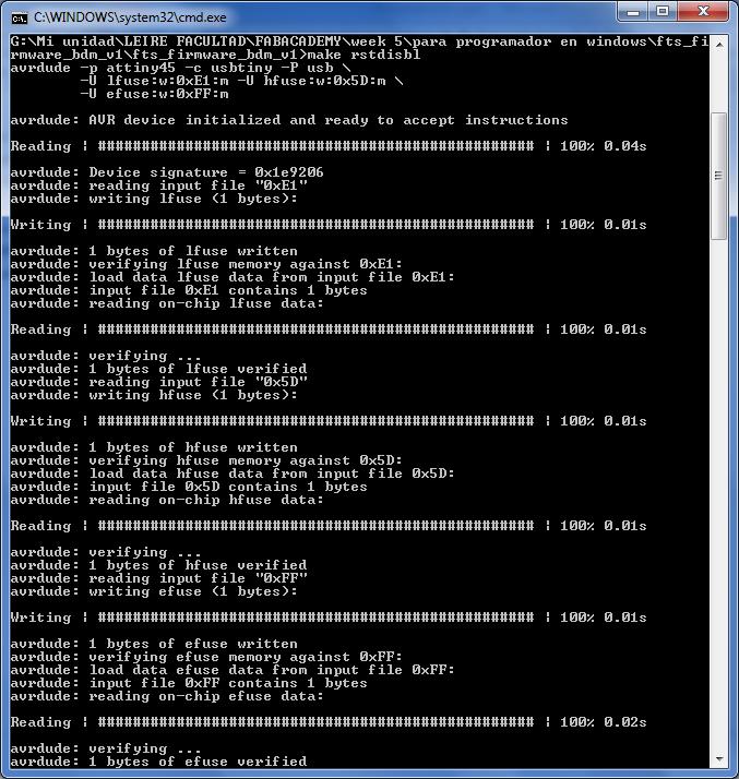
Execute cmd.exe (MSDOS) from Windows, and:
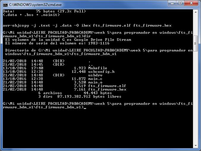
_ cd G:\Mi unidad\LEIRE FACULTAD\FABACADEMY\week 5\para programador en windows\fts_firmware_bdm_v1\fts_firmware_bdm_v1 + enter >> To go to directory of my folder, where I have placed the downloaded files.
_ dir + enter >> to see which files I have in this folder.
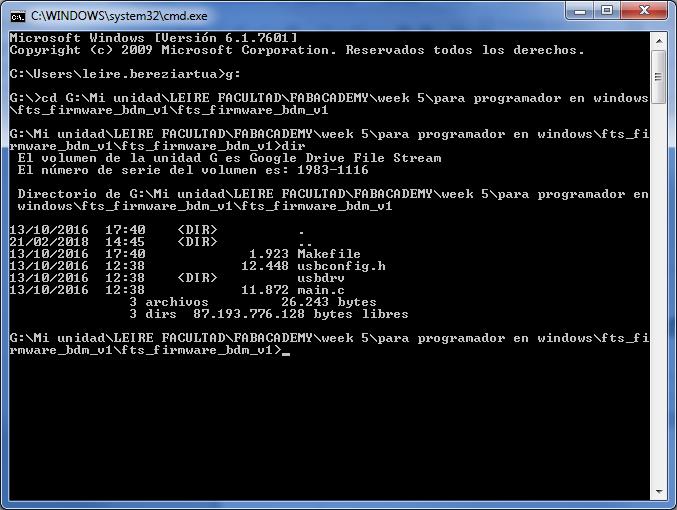
_ make + enter >> to compile, it traduces my “language” to machines “language” (micro-controller).
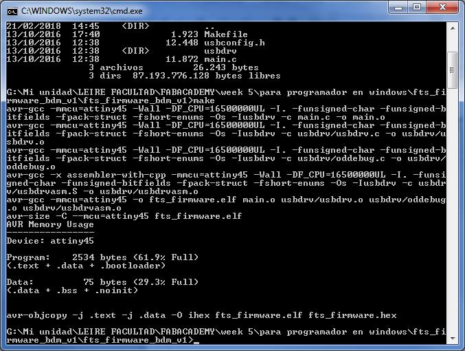
_ dir + enter >> we can see it has created fts_firmware.hex file.
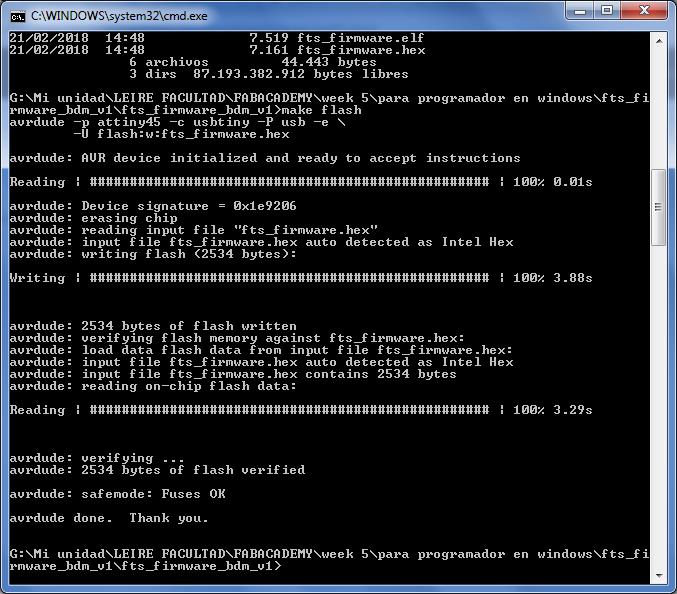
_ make flash + enter >> Uses the programmer connected to program my PCB.
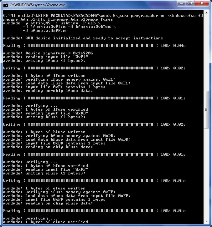
_ make fuses + enter >> Configures PCB to work as as USB.
4. Verify that the board is working properly:
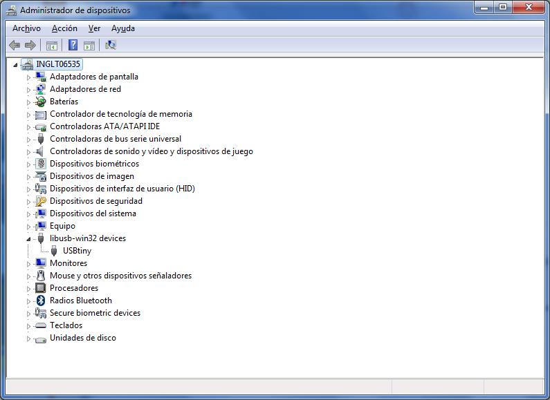
Now, first of doing next step, we have to ensure that PCB is working as an USB. So we disconnect everything, and connect PCB to a computer. Is it recognized?
We could see it in Control panel/System/Devices administration . It has to appear in libusb-win32-devices as USBtinySPI.
If it works well, we connect everything again, and in cmd.exe:
_ make rstdisbl + enter
5. Open up the jumpers to make it a programmer:
And Woala! It has been programmed. Now, last thing is to de-solder the J1 jumper.