
Lingyu Yue @ FAB LAB Szoil · 2018
© 2018 Lingyu Yue · Template by Bootstrapious

This work is licensed under a Creative Commons Attribution-NonCommercial-ShareAlike 4.0 International License.
Electronics Design
- Redraw the echo hello-world board, add (at least) a button and LED (with current-limiting resistor), check the design rules, make it (if you have time this week, test it). (Individual Project)
- Optional: Simulate its operation. Measure its operation.
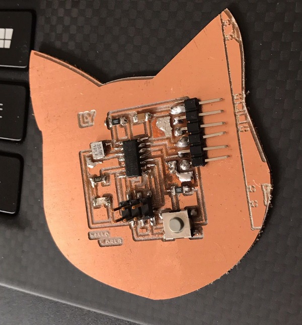
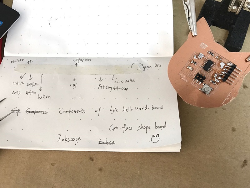
I drew a board with a kitten head outline, it is my first time to make customize outline. It is interesting to draw the ouline with Inkscape. And for this board,I can't find the smaller soldering head, and I was in a rush to solder, the joint was so ugly, I'll improve next time.
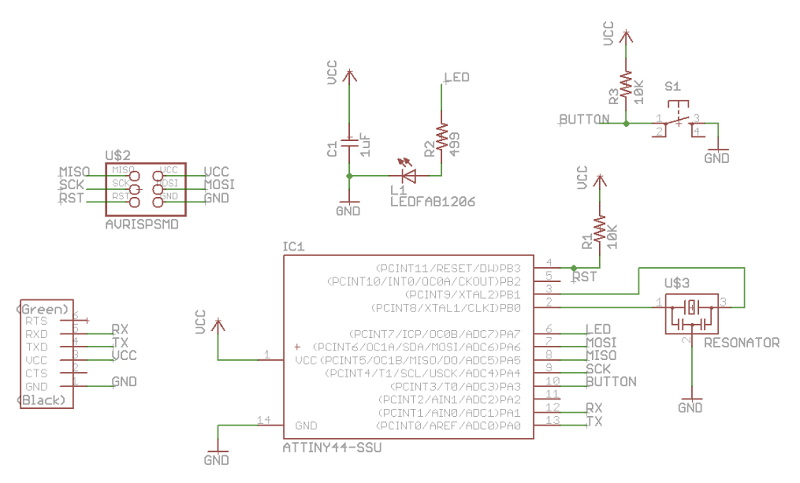
Redrawing the Echo Hello-World board
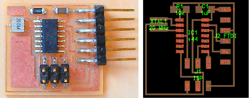
I used Autodesk Eagle 8.7.1 to redraw the Schematic and Board Layout of Echo Hello-World board.
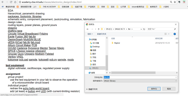
First of all, download the fab.lbr -component library by right-clicking 'Save the link' and adding the library to Eagle installation folder (C:\EAGLE 8.7.1\lbr).
Then, open the Eagle and navigate to Libraries > lbr where you can see the new library marked with the grey small dot. Activate the library by right-clicking it and selecting "Use".
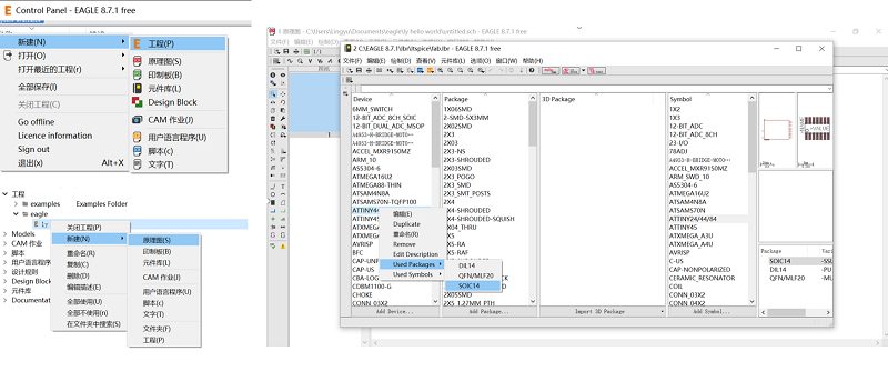
Next, I created a new project by navigating File > New > Project. Then, I created a new schematic by right-clicking the New Project > New > Schematic. After that, I added components to Schematic.
Besides these ones, I addd a button and a LED,
From the supply1 -library I added:
Then I read ATtiny44A datasheet to figure out the pin numbers of the micocontroller.
With the help of my tutor Yufei Ma ,I drew the schematic as below.
I finished the PCB and output this PCB as png format in 2000 dpi.
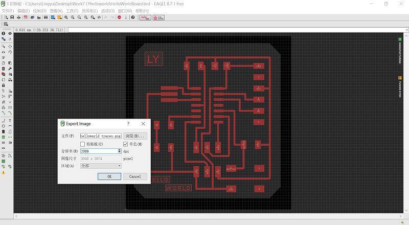
I tried to follow the design rules of drawing a PCB board. Starting from the settings, I did as follows:
Selecting the DRC (Design Rule Check) settings from the toolbar, I defined new values:
- Clearance // set all the 'Different Signals' and 'Same Signal' to be 16mil
- Distance // set Drill/Hole to be 16mil
- Sizes // set Minimum Widht to be 16mil, too
- Supply -tab // set 'Thermal isolation' to be 10mil, and 'Apply'
And then also run ERC option.
When the board layout is finished, select Layers and leave only the Top layer visible. Otherwise there will be some values on the png picture.
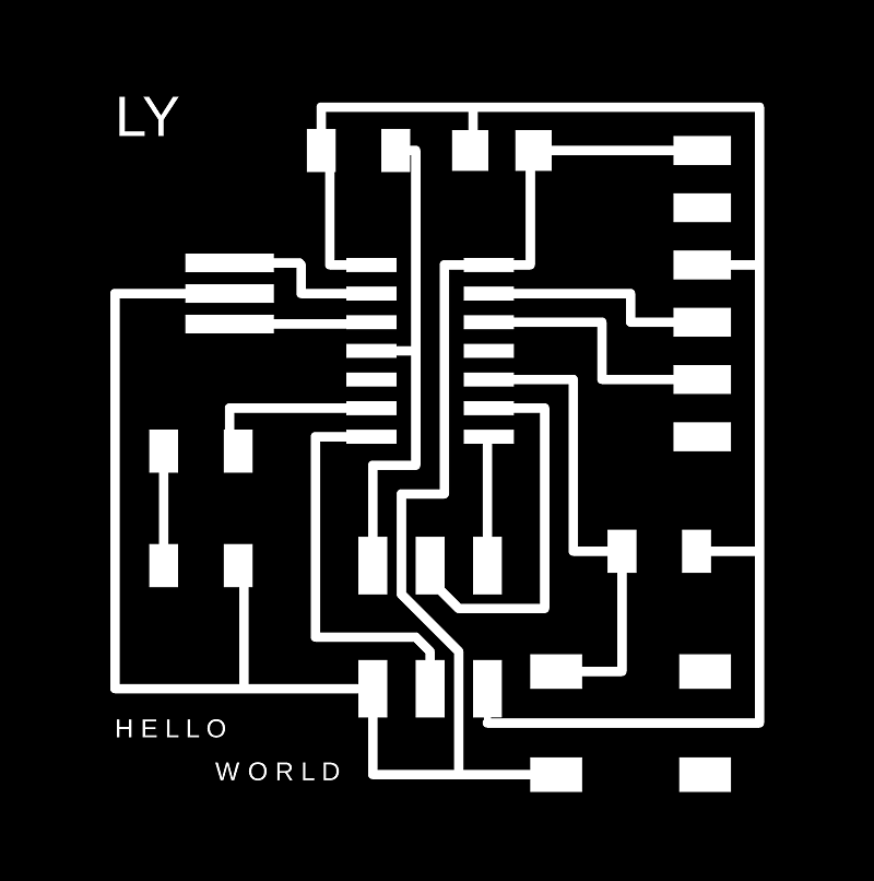
Get .rml -files and Assembling
Creating the .rml files in Fabmodules.org by importing the png file.And then assembled the board.
Here are the design files of LY Hello-World board I made this week.