Week 13: Networking and communication
Group assignment: Send a message between two projects
Individual assignment: Design and build a wired and/or wireless network connecting at least two processors
Individual assignment: Design and build a wired and/or wireless network connecting at least two processors
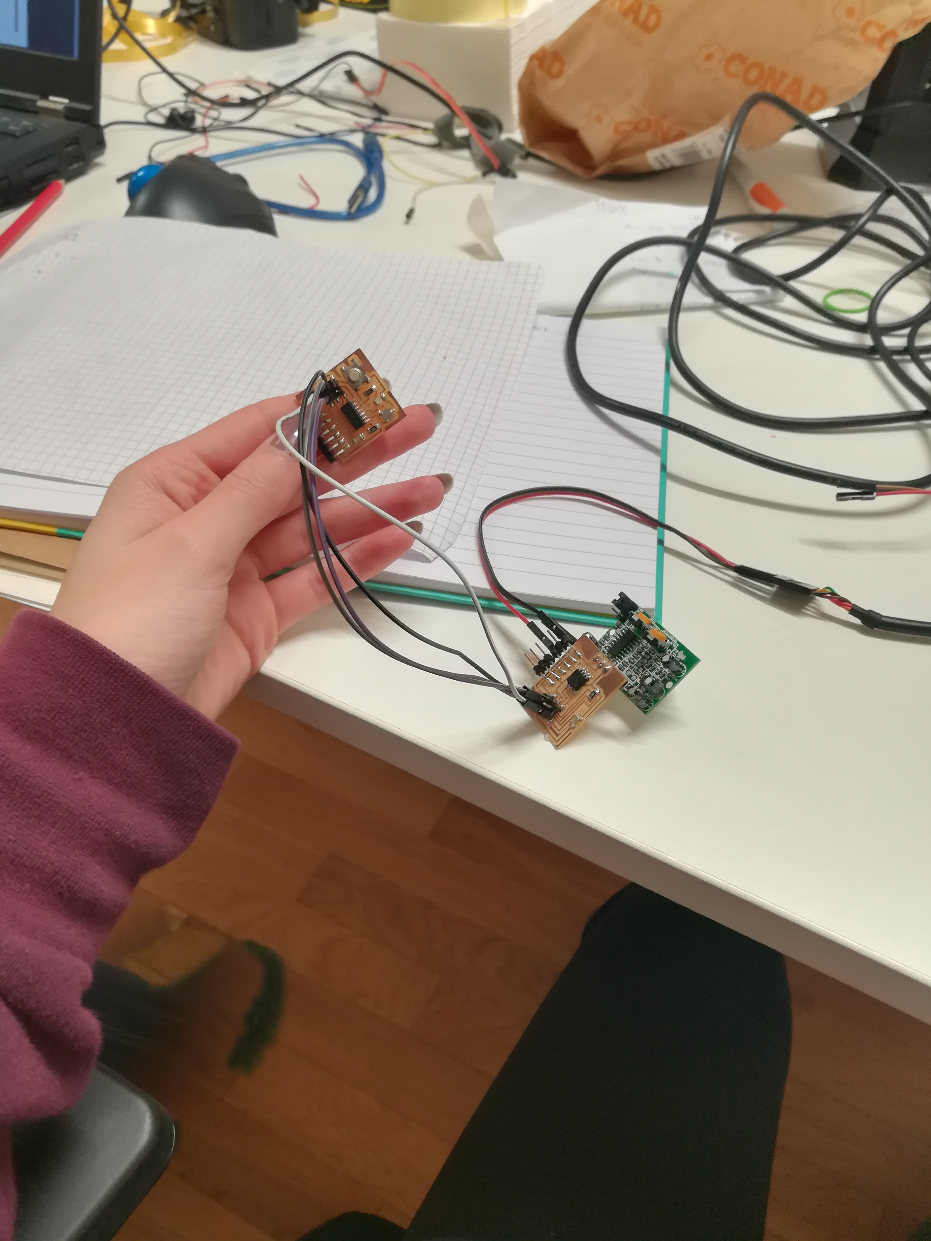
for this week I had to use two boards that I made and connect them with a network
(one is the board I made in the week 10 and the other is the one I made during week 6 ).
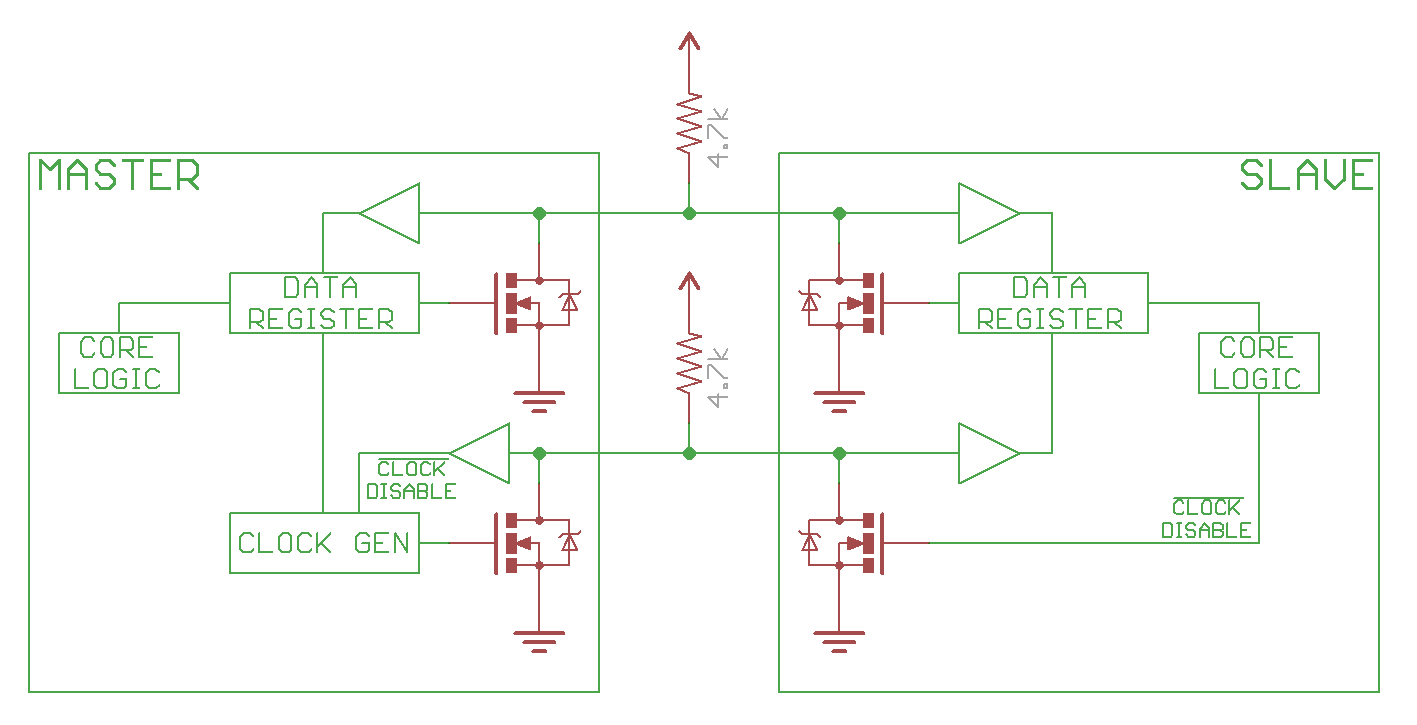
There are a lot of types of Networks, but i chose the I2C protocol.
I2C
The I2C Protocol is a protocol intended to allow multiple slave digital integrated circuits (chips)
to communicate with one or more master chips.
Like the Serial Peripheral Interface (SPI), it is only intended for short distance communications within a single device.
Like Asynchronous Serial Interfaces it only requires two signal wires to exchange information.
How does I2C work?
I2c it's a 2 wire protocol for a 7-bit addressing bus and it's using the SDA line for data transfer and SLC the clock line.
The clock signal is always generated by the current bus master. Some slave devices may force the clock low at times to delay the master sending more data
(or to require more time to prepare data before the master attempts to clock it out).
I took the most important part from this tutorial that explain how Master and Slave will communicate.
"To initiate the address frame, the master device leaves SCL high and pulls SDA low. This puts all slave devices on notice that a transmission is about to start.
The address frame is always first in any new communication sequence. For a 7-bit address, the address is clocked out most significant bit (MSB) first, followed by a R/W bit indicating whether this is a read (1) or write (0) operation.
The 9th bit of the frame is the NACK/ACK (Not Acknowledge/Acknowledge) bit. This is the case for all frames (data or address). Once the first 8 bits of the frame are sent, the receiving device is given control over SDA. If the receiving device does not pull the SDA line low before the 9th clock pulse, it can be inferred that the receiving device either did not receive the data or did not know how to parse the message. In that case, the exchange halts, and it’s up to the master of the system to decide how to proceed.
After the address frame has been sent, data can begin being transmitted. The master will simply continue generating clock pulses at a regular interval, and the data will be placed on SDA by either the master or the slave, d epending on whether the R/W bit indicated a read or write operation.
Once all the data frames have been sent, the master will generate a stop condition by a 0->1 (low to high) transition on SDA after a 0->1 transition on SCL, with SCL remaining high. During normal data writing operation, the value on SDA should not change when SCL is high, to avoid false stop conditions.""
for my project I will program my boards so that the master sends to the slave a value and this value is read by the slave, that will emitt a blink. Onestly for this project Simone Guercio helped me a lot.
Since the boards have AtTiny processor, this influenced the sketch's realization so I downloaded and installed the library from github, this for the master and this fore the slave. After this I made the sketches:
Master
I took the most important part from this tutorial that explain how Master and Slave will communicate.
"To initiate the address frame, the master device leaves SCL high and pulls SDA low. This puts all slave devices on notice that a transmission is about to start.
The address frame is always first in any new communication sequence. For a 7-bit address, the address is clocked out most significant bit (MSB) first, followed by a R/W bit indicating whether this is a read (1) or write (0) operation.
The 9th bit of the frame is the NACK/ACK (Not Acknowledge/Acknowledge) bit. This is the case for all frames (data or address). Once the first 8 bits of the frame are sent, the receiving device is given control over SDA. If the receiving device does not pull the SDA line low before the 9th clock pulse, it can be inferred that the receiving device either did not receive the data or did not know how to parse the message. In that case, the exchange halts, and it’s up to the master of the system to decide how to proceed.
After the address frame has been sent, data can begin being transmitted. The master will simply continue generating clock pulses at a regular interval, and the data will be placed on SDA by either the master or the slave, d epending on whether the R/W bit indicated a read or write operation.
Once all the data frames have been sent, the master will generate a stop condition by a 0->1 (low to high) transition on SDA after a 0->1 transition on SCL, with SCL remaining high. During normal data writing operation, the value on SDA should not change when SCL is high, to avoid false stop conditions.""
for my project I will program my boards so that the master sends to the slave a value and this value is read by the slave, that will emitt a blink. Onestly for this project Simone Guercio helped me a lot.
Master and slave
Since the boards have AtTiny processor, this influenced the sketch's realization so I downloaded and installed the library from github, this for the master and this fore the slave. After this I made the sketches:
Master
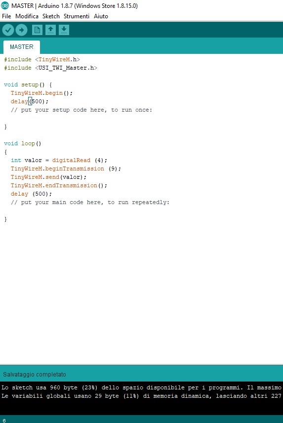
Basically the master with TinyWireM.beginTransmission connects with the slave with the same number.
TinyWireM.send sends a value to the slave.
Slave
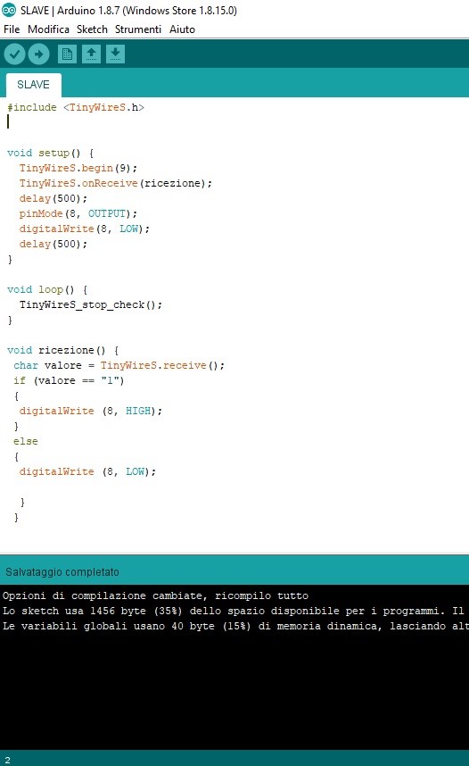
With TinyWireS.onReceive the slave knows that when it receives the value number 1 the led will be on, otherwise it will be off.
After I uploaded the sketches I connected the master to the FTDI (only ground and vcc) cable and the slave to the SPI through 4 cables. Fortunately it worked at the first time
Serial communications
in this type of communication the information travel one bit at time