Assignment
- Redraw the echo Hello-world board
- Add a least a button and LED (with resistor)
- Make-it and Test-it
Redrawing the board
To redraw the board is necessary to use a PCB design and schematic software as
Eagle . Which I'll use for this assignment.
Eagle is available for free if you open an Autodesk account and you'e student or a teacher (which is my case)
and runs in windows and Linux.
The steps to create a PCB (Printed circuit boards) in Eagle are: 1. create the schematic file, 2. Generate the board and
3. create the routes between the components.
Creating the schematic file
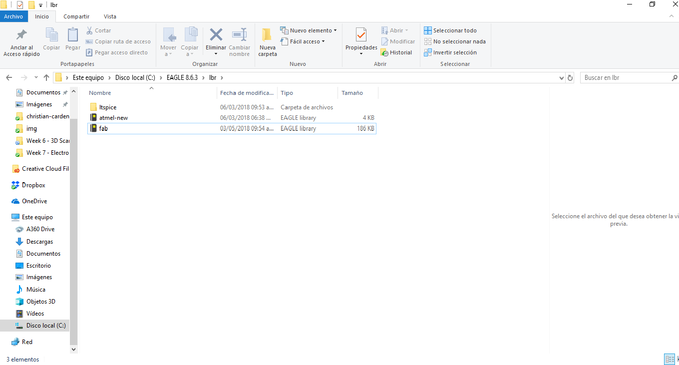
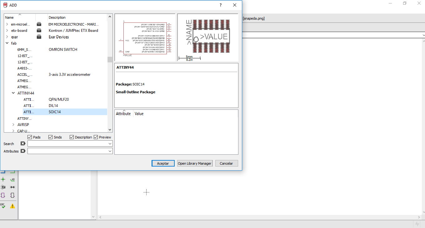
To create the schematic is necessary to add the library with the main components
used in any Fab Lab. This library is called fab.lbr, and install libraries is
very simple in eagle, copying the library file in the folder called lbr in eagle installation folder is enough. (Figure 1).
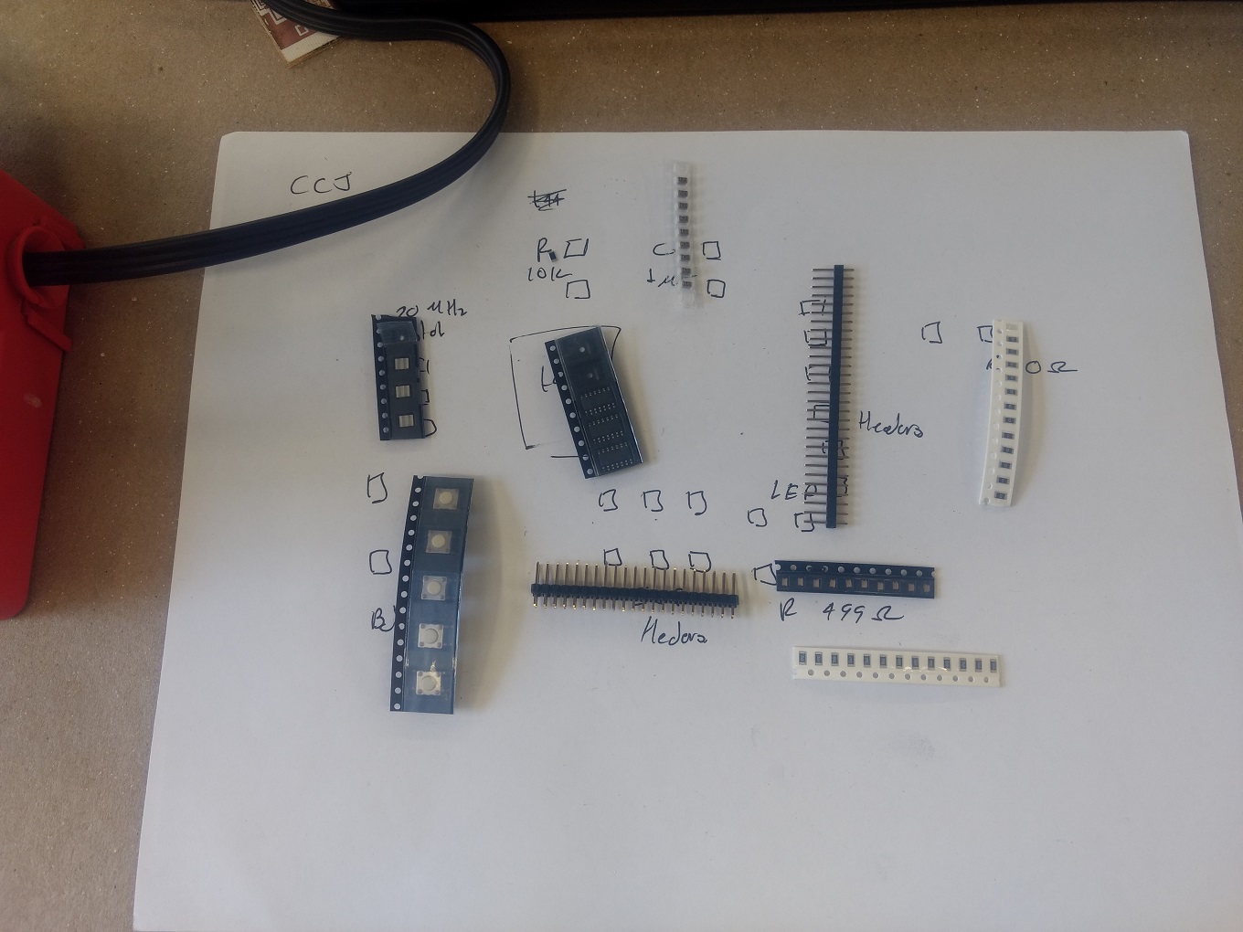
Once the library is installed the components of the board must be add to the schematic board (Figure 2). The components used are listed in the next table.
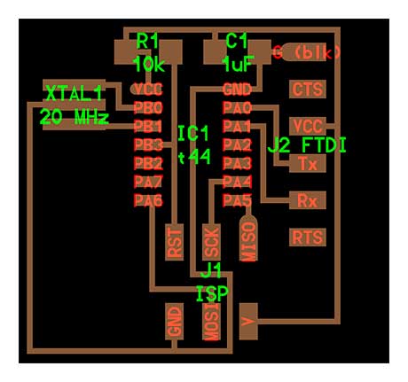
These components were selected according to the original Hello-world board (Figure 3) and the assignment which require add at least one button and one LED (with resistance).
| Components | Qty | Comments |
|---|---|---|
| Attiny 44a | 1 | -- |
| Crystal 20 MHz | 1 | -- |
| Resistance 10 KΩ | 1 | -- |
| Capacitor 1 µF | 1 | -- |
| ISP 6 Pin Header | 1 | -- |
| FTDI Header | 1 | -- |
| LED | 1 | New component |
| Resitance 330 Ω | 1 | New component |
| Resistance 0 Ω | 1 | New component * |
With the components in the schematic board (Figure 4) is necessary to make the connection between them. I found very useful to name or assign values to the resistors and capacitors, this way is easier to identify them and avoid mistakes during the creation of the net. The net that I made (Figure 5) was based in the hello-world board. The new components were added to the electrical network (or electrical circuit) using the available pins in the microcontroller.
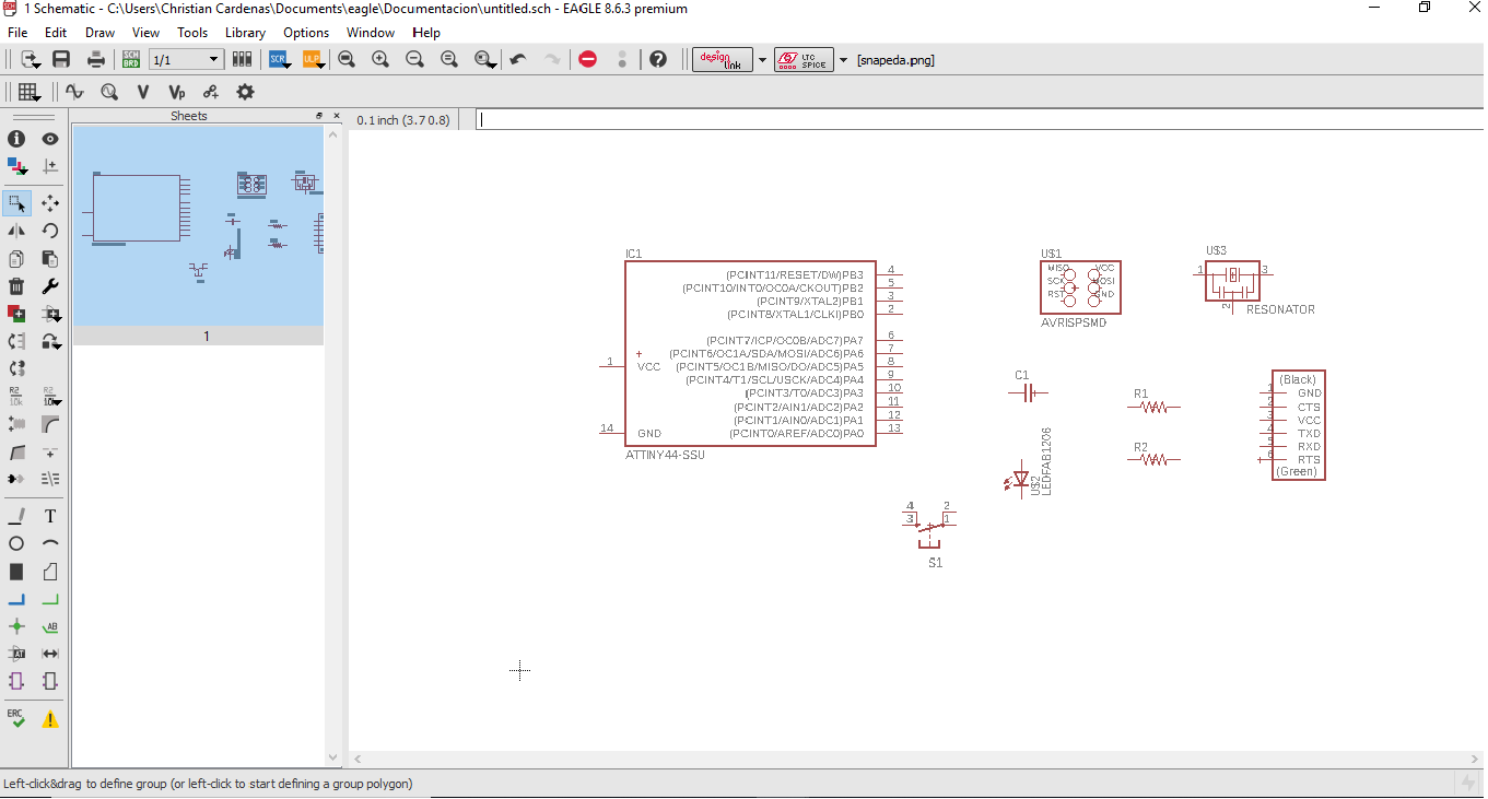
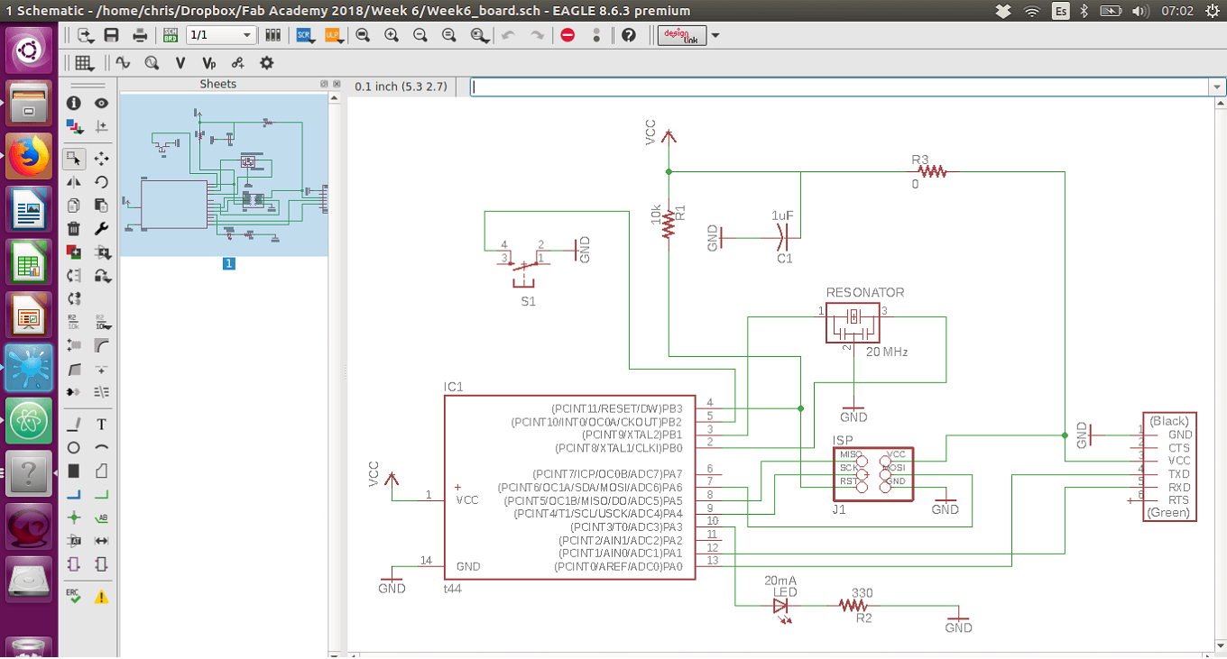
The LED with its 330 ohm current limiting resistor (The resistance value was calculated according to Ohm's law: V = IR; assuming 5 Volts, and 20 mA current) is connected to PA3 pin (number 10) and ground. The button is connected to PB2 pin (number 5) and ground. The zero resistance was added after some difficulties while tracing the route which is the next step.
Creating the Board file
With the schematic file complete (components and net) create the board file is easy with
eagle. Is enough with press the Generate/Switch to board button or in the menu File – Switch to board. With this command a new
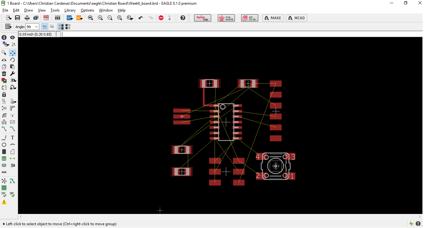
board is showed with the footprint of the components and yellow lines showing the connection that must be make (Figutre 6).
To trace the route there’s two options: 1) let the software do it (via autorouter) or 2) do it manually. I choose to do it manually according to
the recommendation of Neil and Ivan (my local instructor). Also as a newcomer in electronics for me was a good idea to increase
the track width to 24 mil and choose wire style bend 0 (only 90 degrees turns). This can be helpful specially in the moment of
welding the components.
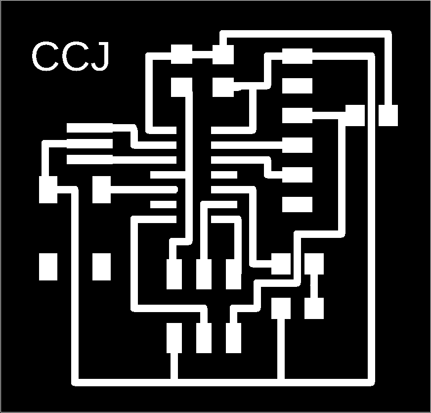
Before tracing the routes is also a good idea to limit the area only where the components are and also try different arrangements
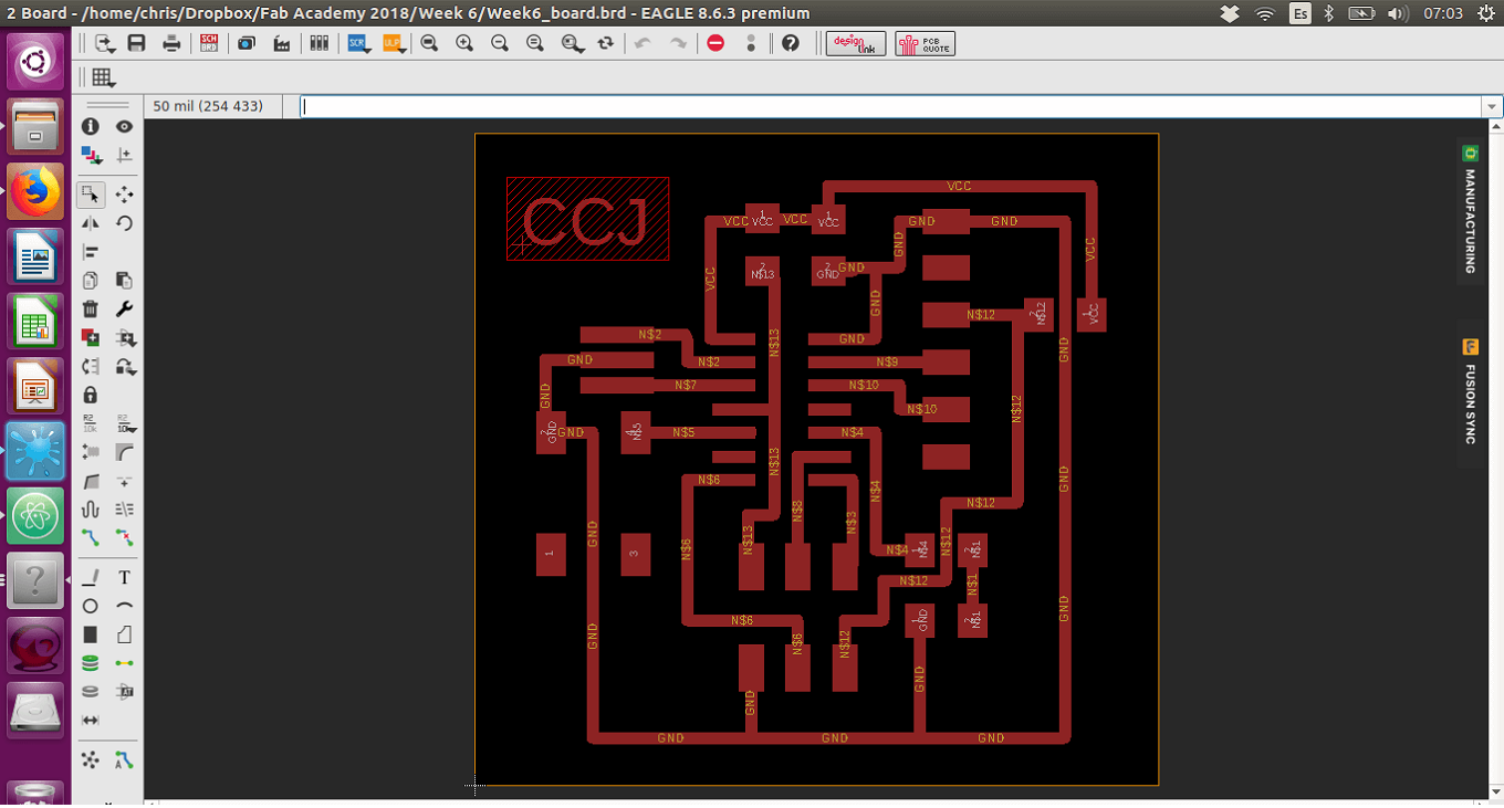
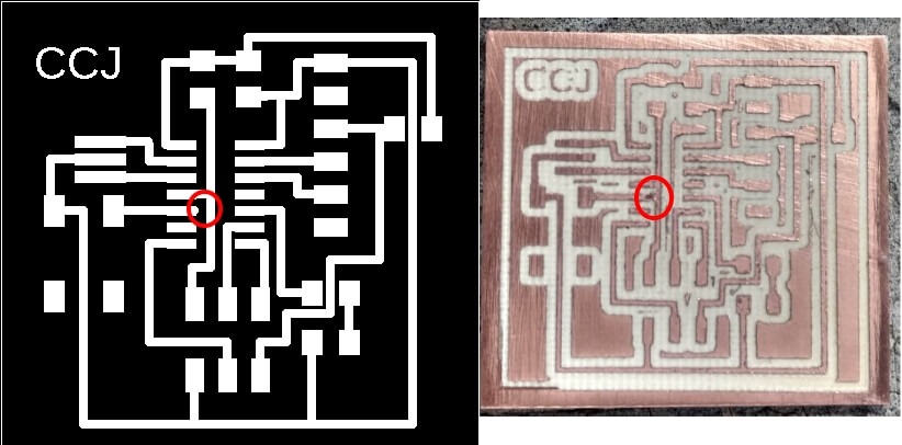
of them until the routes and easy to trace. Finally, after several attempts all the traces were done and checked with ERC and DRC;
and the board is ready to export as an image. (Figure 7).
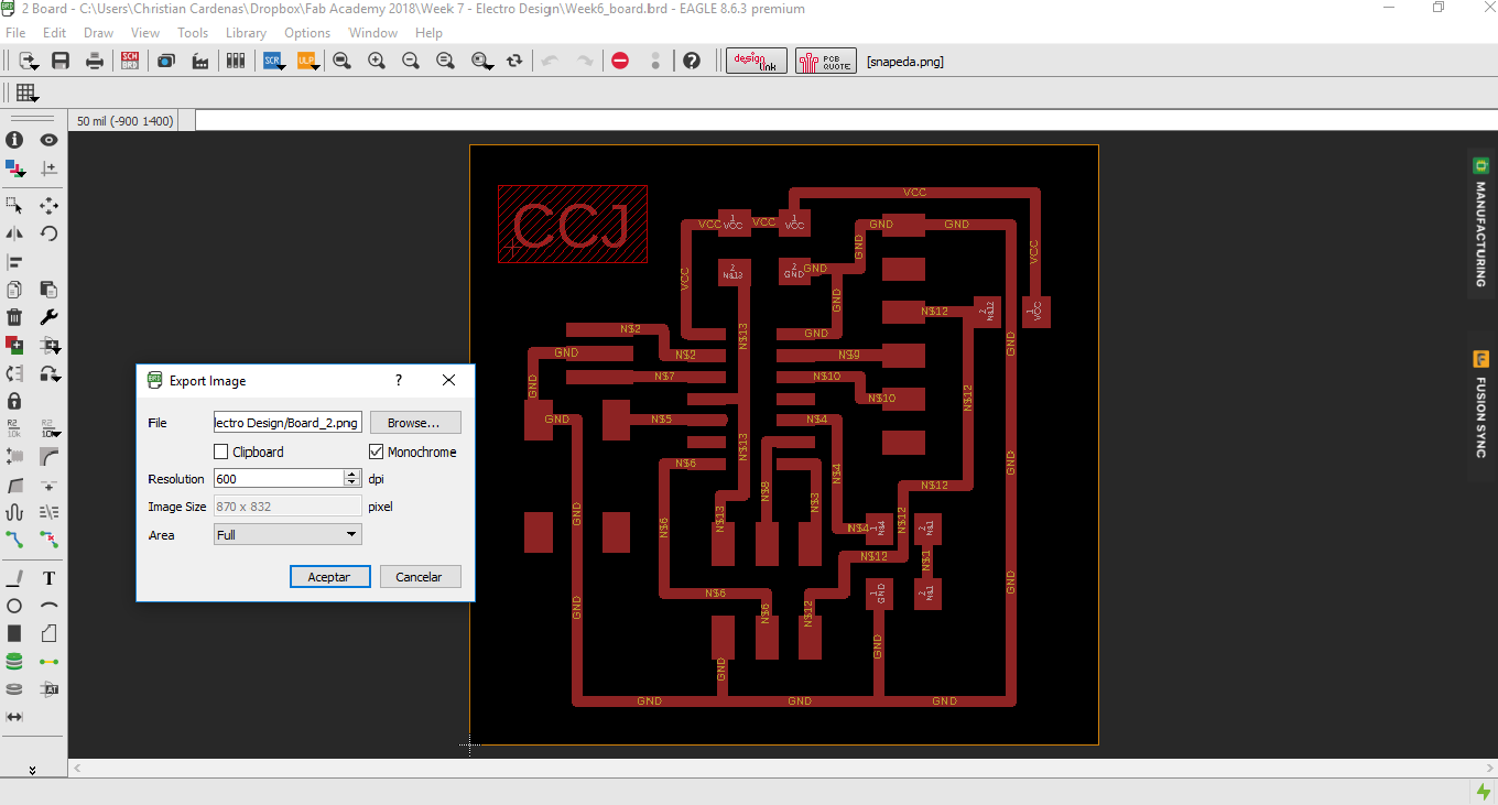
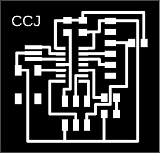
To obtain the image must be made through export (File – Export – image) and set the conditions for the image. I found the conditions set in the Figure 8 the best to work with fab modules.
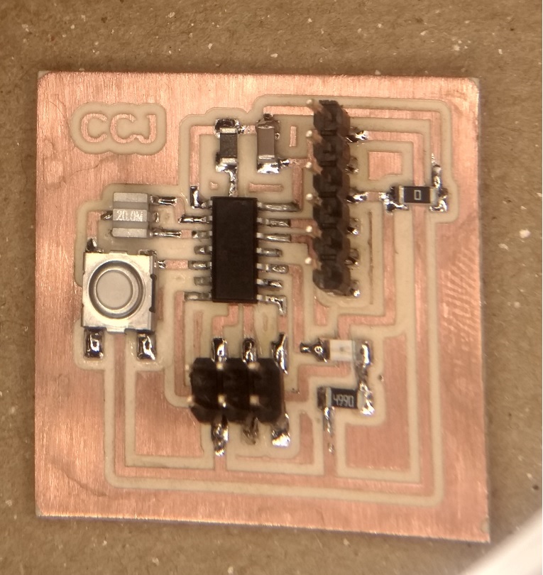
Making the PCB
Following the procedure describe in Week 5 the Board was make (Figure 10). Following the procedure describe in Week 5 (link) the Board was make (Figure 10). Further inspection of the board I found a defect in the board some of the tracks were separated (Figure 11). I Fixed this paper cutter just applying pressure to the copper layer and creating the gap between these tracks.
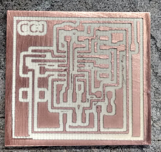
The PCB can be seen in Figure 13