TODO LIST
- Group project : use the test equipment in your lab to observe the operation of a microcontroller circuit board
- Redraw the echo hello-world board add (at least) a button and LED (with current-limiting resistor) check the design rules, make it, and test it
Introduction
This week assignment is mainly aimed at to learn and understand any of the PCB designing tools. I need to redesign the echo hello world board. I normally use Autodesk Eagle CAD tool to design all my PCBs. So decided to go with Eagle PCB. We also have a group assignment to do, We need to use and test the equipment in your lab to observe the operation of a microcontroller circuit board.
Printed Circuit Boards
Printed circuit board is the most common name but may also be called “printed wiring boards” or “printed wiring cards”. Before the advent of the PCB circuits were constructed through a laborious process of point-to-point wiring. This led to frequent failures at wire junctions and short circuits when wire insulation began to age and crack.
A significant advance was the development of wire wrapping, where a small gauge wire is literally wrapped around a post at each connection point, creating a gas-tight connection which is highly durable and easily changeable. As electronics moved from vacuum tubes and relays to silicon and integrated circuits, the size and cost of electronic components began to decrease. Electronics became more prevalent in consumer goods, and the pressure to reduce the size and manufacturing costs of electronic products drove manufacturers to look for better solutions. Thus was born the PCB
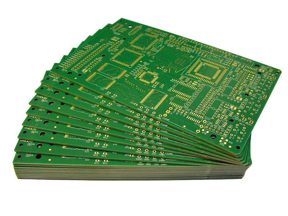
PCB is an acronym for printed circuit board. It is a board that has lines and pads that connect various points together. In the picture above, there are traces that electrically connect the various connectors and components to each other. A PCB allows signals and power to be routed between physical devices. Solder is the metal that makes the electrical connections between the surface of the PCB and the electronic components. Being metal, solder also serves as a strong mechanical adhesive.
Different Types Of PCB Material
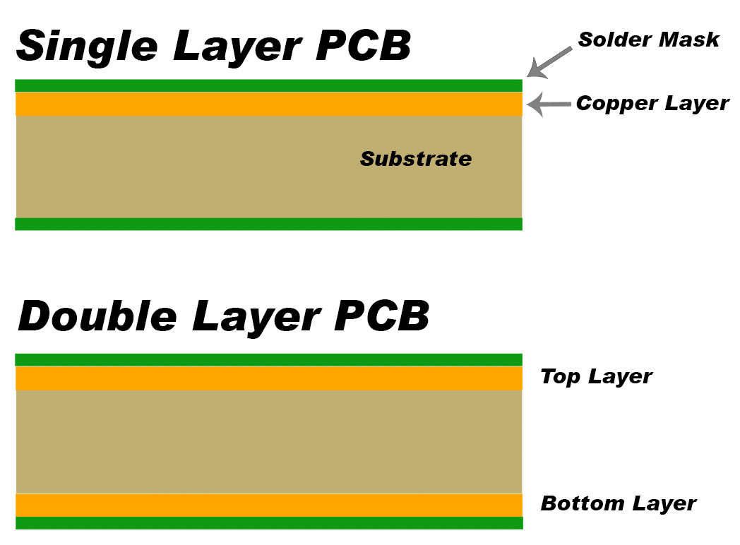
Different types of PCBs are available in the market. Both single sided and Multiple sided PCB are Using in the industry. The common using PCB is Single sided and Double sided PCB. PCBs are manufacturing with different types of materials like epoxy, fiberglass, ceramic etc... for the substrate layer.
The materials are chosen for the purpose and use case. However, We are using a pcb with FR (Flame Retardant). A fiberglass and epoxy laminated PCB. There are different grades of FR GRADE PCBs FR1,FR2,FR,FR4 etc We are using FR1 Grade PCB in Fablab Kochi.
FR 1 : Flame Retardant
The family of laminates under the name FR-1 and FR-2 by the NEMA (National Electrical Manufacturers Association, USA) classification. These materials are made from paper and phenol compounds and are used only for the production of single side printed circuit boards. FR-1 and FR-2 has the similar parameters, the main difference is that FR-1 has a higher glass transition temperature Tg. Because of the similarity of the parameters and applications of FR-1 and FR-2, many of the material suppliers produce only one type of laminates, most often FR-1. Laminates have a good ability to mechanical processing (milling, punching). Flammability rating is UL94-V0. To know more about FR-1 Vist here
FR-1/FR-2 laminates are divided into the following subclasses:
- Halogen-free, without phosphorus and antimony, non-toxic
- With normalized index of CTI ≥ 400, ≥ 600
- Non hydrophobic
PCB Designing
PCB designing is a process of designing physical connection of the circuit. The PCB designing will start from Schematics designing. To design PCBs, We have a lot of PCB designing CAD tools available. Both professional and beginner level tools are available. It is upon you, to choose the best for you. The schematic design is a representation of physical circuits and connections. We can add the components by picking from the component library. If you need a custom component library that doesn't come in your PCB designing tool's library. You can design your own component in the library editor in some PCB designing tools. After adding the components you can virtually do the connection using wiring tool or Net tool. After designing schematics the next stage is to Designing the PCB physical connection of the PCB by routing the Traces using trace tool. You could also change the Designing rules to your needs. You can do this using both manual routing and Auto Routing. Auto-routing did by the computer but in some cases, it is best to do manually routing the traces. After the PCB designing process, we can export the PCBs. The most software outputs into the GERBER Files, But different output files are supported by different software. The GERBER file is an open ASCII vector format for 2D binary images. It is the standard file format used in PCB manufacturing industry. But at FabLab, we are using Modela MDX20 Milling machine. So, we need PNG image. Here are some PCB Designing CAD tools. I'm Using Eagle PCB developed by Autodesk.
My Fav Tool : Eagle PCB
When it comes to PCB designing, I always prefer Eagle PCB. Eagle (Easily Applicable Graphical Layout Editor) developed by CADSOFT but now it is acqured by Autodesk. Eagle is free for students, hobyyists and teachers. But both premium and professional versions are also vailable. In my experience, Eagle is simple to use and have a large community support and Eagle is also easy to learn. Both professional and hobbyists are using Eagle PCB for their use. It is suitable for simple and complex PCB designing. You you wanna try on Eagle, follow this Documentation.
Eagle Work Flow
- Schematics Designing
- Component Library & Library Editor
- Board Designing & Layouting
- Check Design rules and ERC errors
- Give proper Board Dimension Outline and export as PNG file
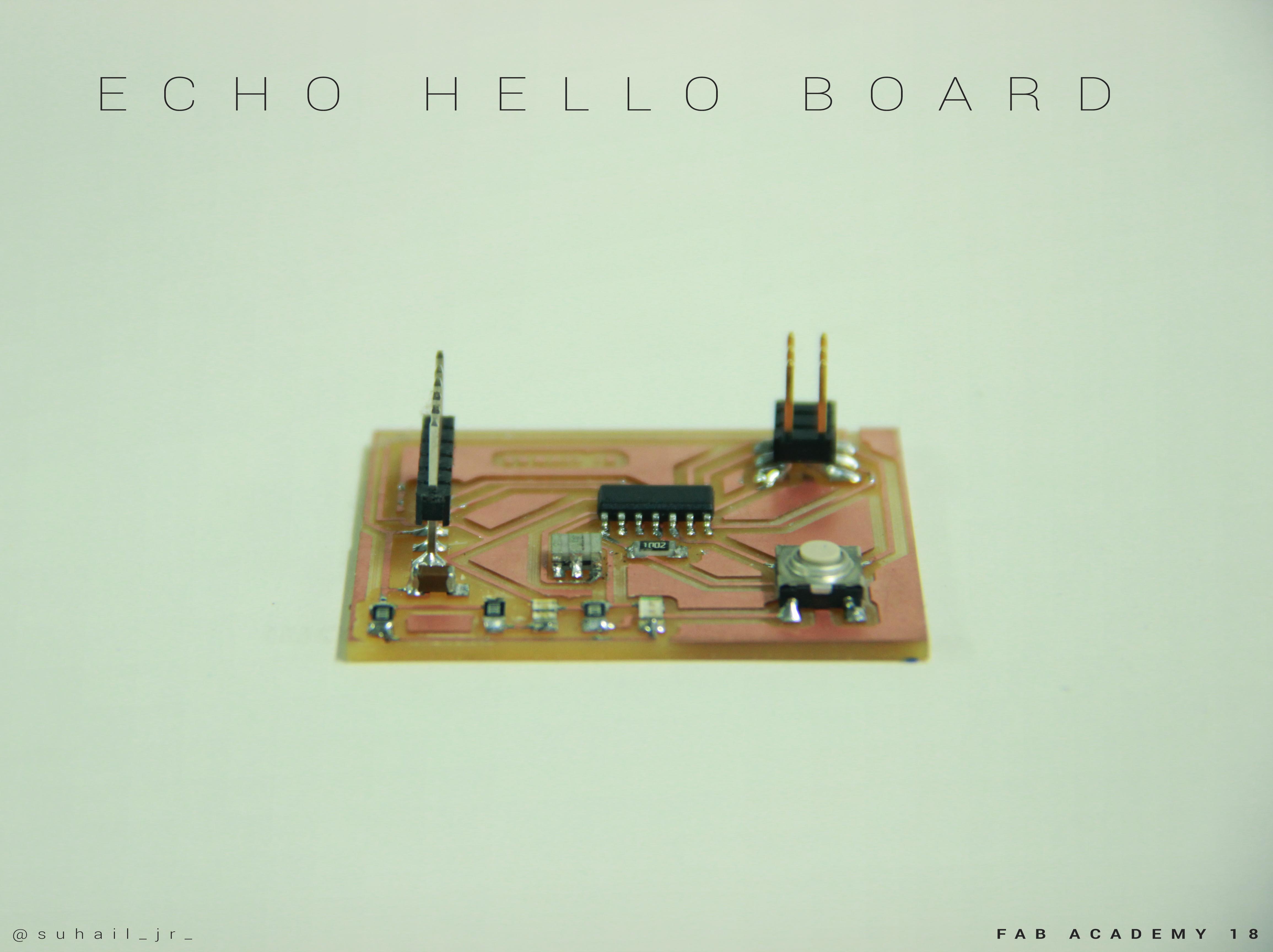
Designing Echo Hello World Board
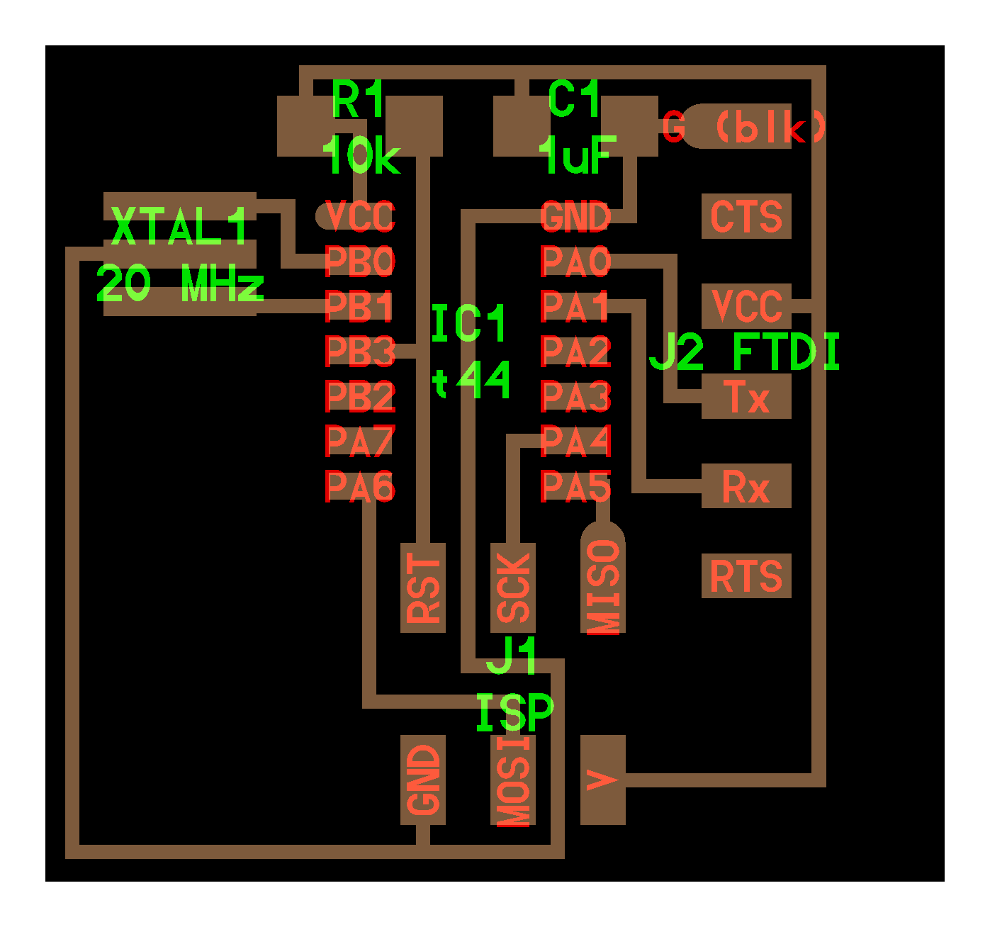
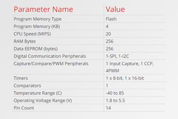
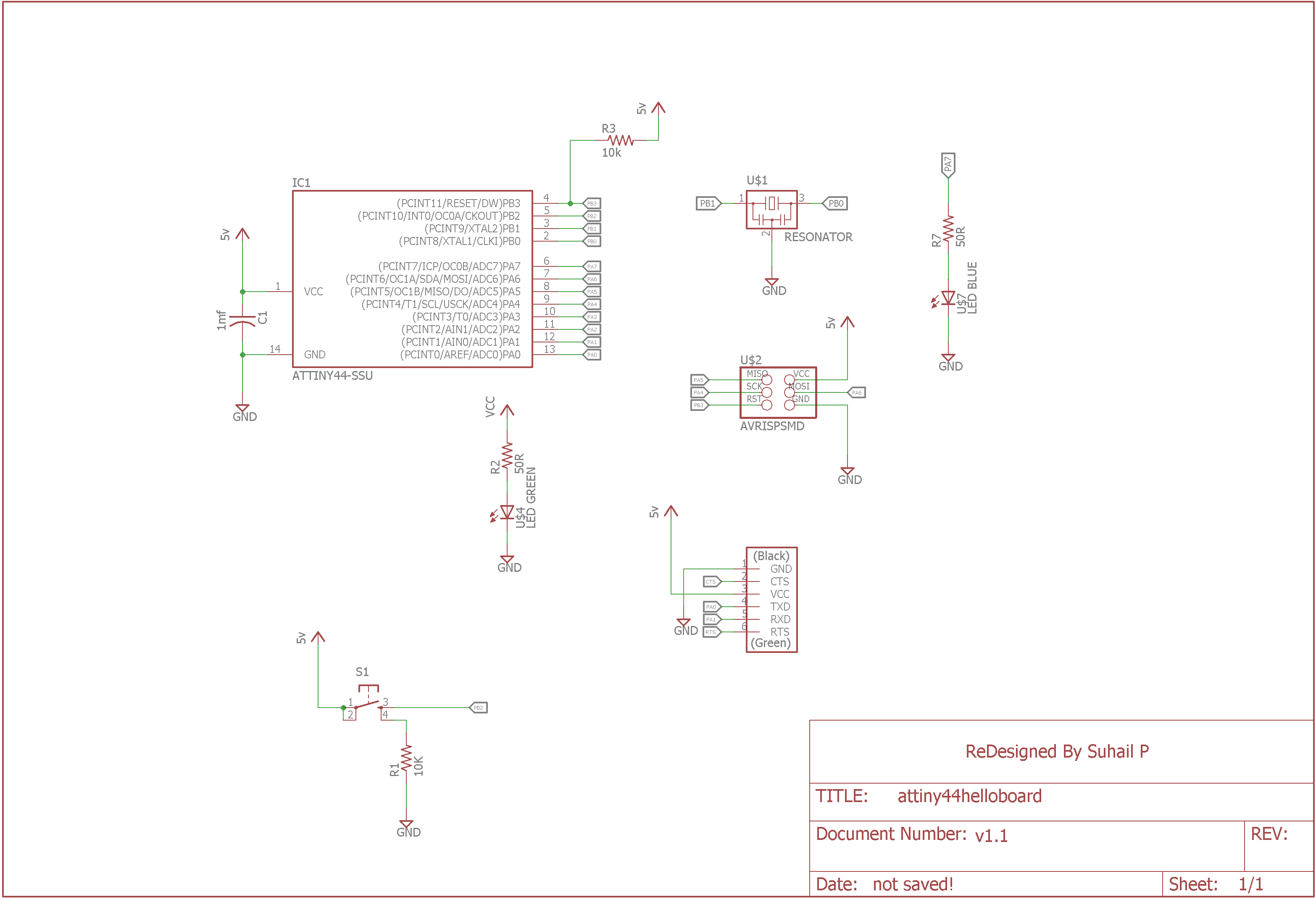
The Echo hello board is a Attiny44 based board. So first i downloaded the Attiny44 Documentations and datasheet from here. I go through the features and pin configruation and got a overall idea about Attiny44.
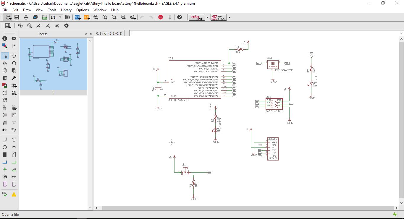
Then i opened the Eagle PCB software and select the new project and named it Fab projects (you can name it anything you want, but use a memorable one). Then i started with a New schematics with in the project. Before designing the Schematics i need some components library that doesn't comes in eagle default component library. Fortunatly Fab Foundation have its own Eagle library called fab.lbrfor all the components that available in the Fab inventory. You can download from Fab.lbr I downloaded in to my PC. To use the library, first you need to add the Fab.lbr into the library manager.
Steps to Add Library to Eagle
- Hover over your mouse cursor on the library tab on the top center of the window
- Then Open Library Manager
- Click on Browse Library
- Browse your downloaded Library
- Click on Open
- Click on Update
So now, i need to place all the components to the schematics designing window.
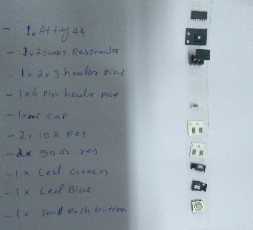
Components List :
- 1 x ATtiny44-SSU
- 1 x 20mhz resonator
- 2 x Resistor-10K
- 1 x Capacitor-1uF
- 1 x AVR ISP Header SMD
- 1 x FTDI Header
- 1 x Switch Omron 6mm
- 1 x Green LED SMD
- 1 x Blue LED SMD
- 2 x Resistor100-Ohm
Virtual Parts :
- VCC
- GND
Now, i started to conect the components each other properly. I used Label Tool to avoid some complicated wiring. You can also do to conect the component pins each other without using wire tool and Net tool. The Nets with same name will automatically get conected. What i updated in the board is ,I conected a omron switch along with a pull down resistor to the PB2 and Conected a LED with a current limiting resistor to the PA7. I also added a power indicator LED along with a current limiting resisitor.
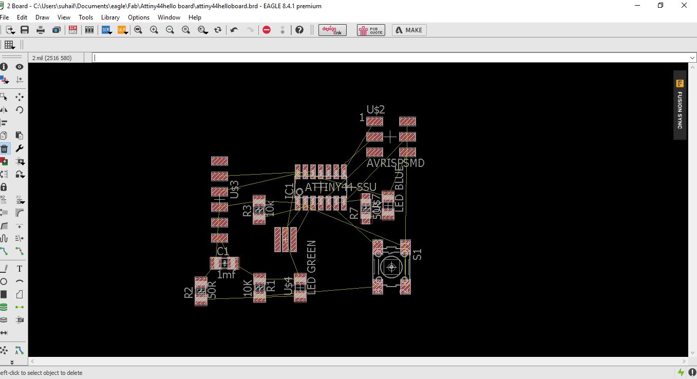
After design the schematics part. Now i need to design the PCB layout, by clicking on the button "Generate/switch to board". I arranged all the components properly and closest each other.
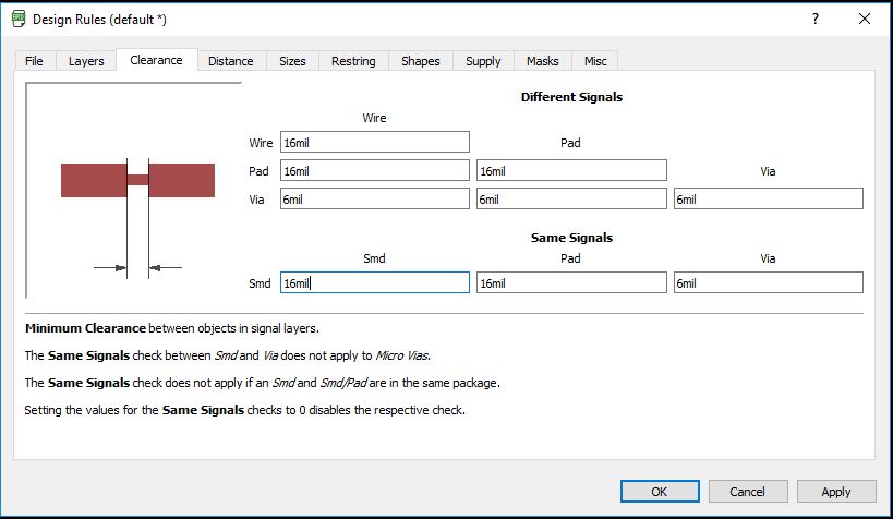
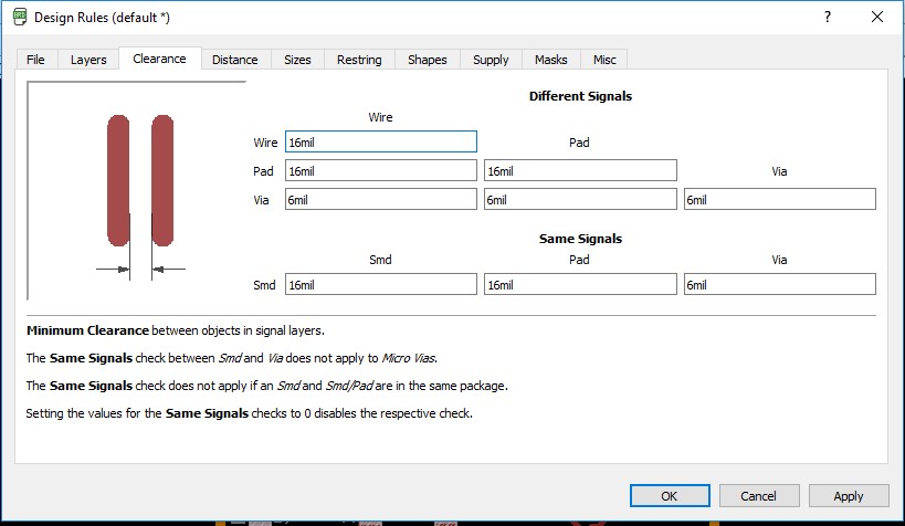
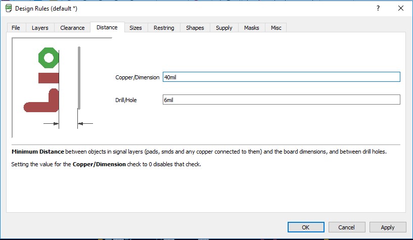
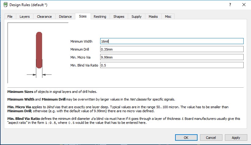
Before routing, I need to Change the Design rules. Do you think why i need to?. Design rules is the important part of PCB designing. We have 1/64 bit to mill the PCB and 1/32 to cutout the PCB. So i need to change some parameters in Design rules. The equalent value of 1/64 = 0.4mm (15.7) and 1/32 = 0.8mm (31.4). Here is the screenshot of my design rules window.
Now i need to route all the trace, I arranged the components much close that possible. Then tried the Auto Routing. But three traces doesn't routed by the computer. Its mostly because of the design rules. But i can't change design rules.
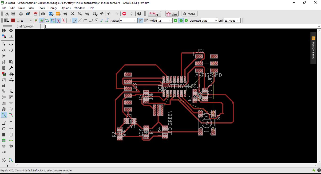
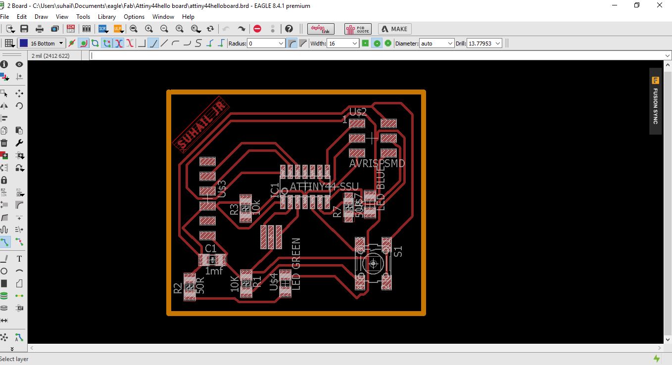
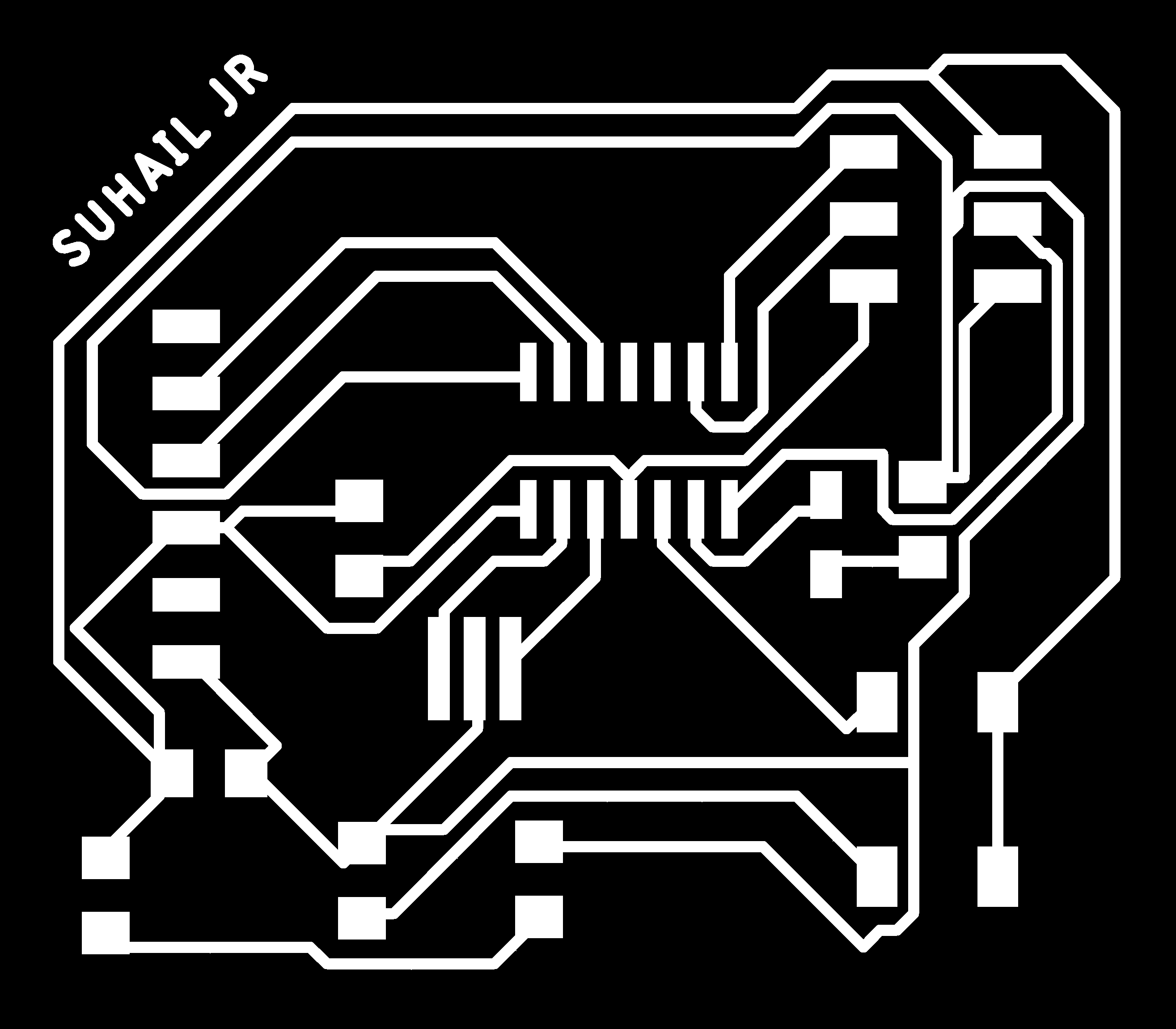
The routing is little bit tricky. I rearanged some components and did a Auto routing once again. But still two of the traces doesn't routed successfully. So manually routed them. This time its done. I also drawn the outline of the PCB with a width of 0.8mm. Here is the screenshot of the completed routing.
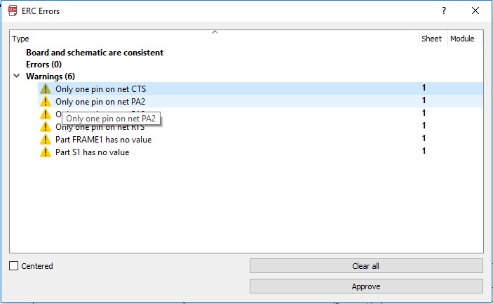
DRC and ERC check
Before milling the final board design, i need to design rule check and electronics rules check. You can view them in the below images. I have got some warning while in ERC check, but it id the common warnings like value missing, name missing etc... it wont effect the working of the circuit.
Final Schematics
Final Board Trace Layout

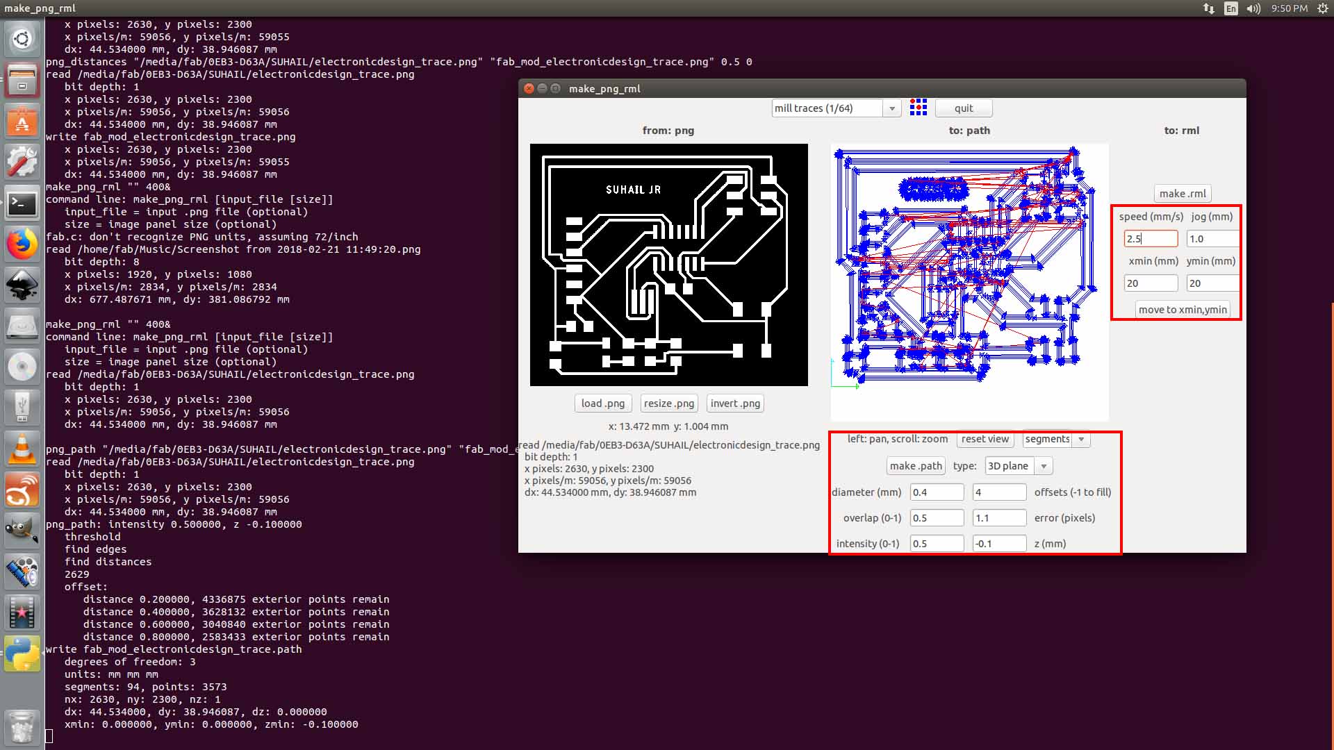
Download the resource File for This Week

Milling The Board Using PCB Milling Machine
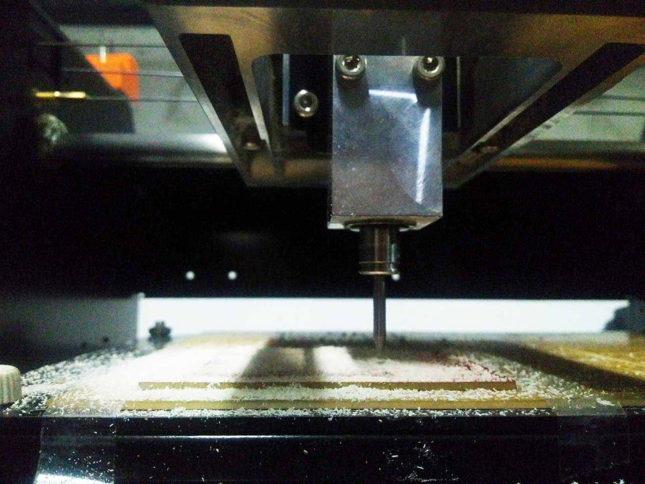
Now i need to Mill the Board. I explained how to mill the board in the Electronic Production Week. Nothing more in this section, i just followed the PCB milling with the 1/64 bit. Then set the X and Y parameters. Then i usual made the tool path and send into the machine. The mechine took almost 20minutes to millout the PCB and almost 2 minutes to cutout the PCB.
The milling is almost take upto 20 minutes approximatly. So, i go for a coffee. After milling and cutout the PCB. I immediatly started to the Soldering section.
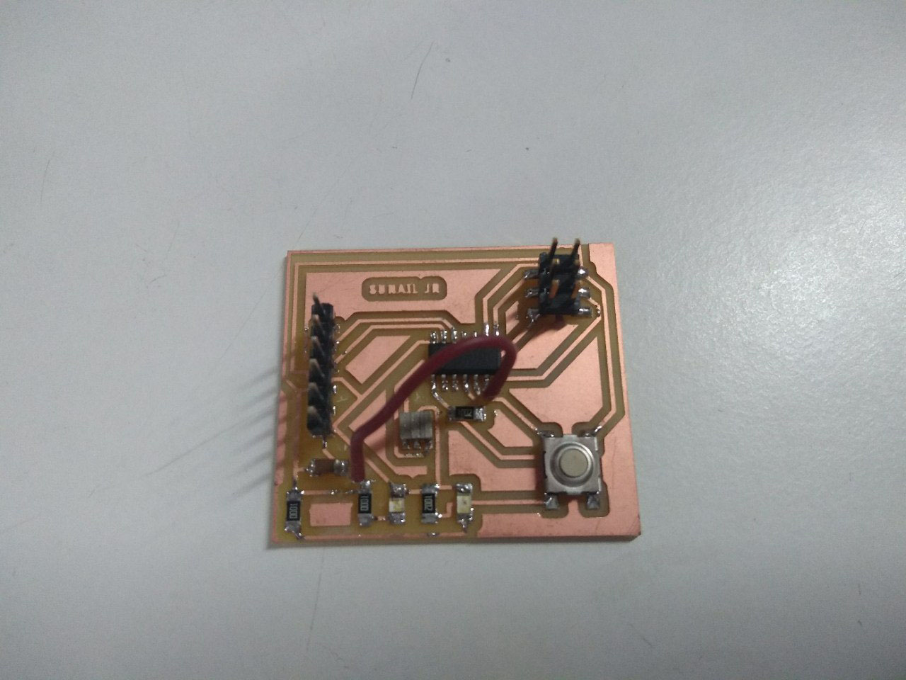
Soldering Echo Hello Board
First i need to Collect the necessory components for my Echo Hello Board. I already said the Components that used in schematics. All i need to do is collect the Components and solder them on the PCB.
I started to solder components on the PCB. As usual i soldered the Attiny44 on the PCB first. Then i soldered the Resonator. May be for beginers Soldering SMD resonator little hard, because of its footprint. I have a simple trick to do the soldering of the resonator. Just heatup and solder the pads then place the resonator carfully on the pads. Then once again heatup the three pads same time. It took 4 second to heatup the three pads in a 300 degree celcius temperature. The Resonator easly place on the pads. Take care of the over heating the pads or resonator. if you over heat one of them. The pads will ripoff. After soldering resonator i go for other components. The did'nt have the FTDI pins that available in the FAB inventory. Because it is already over. So we got alternative Trhrough Hole Male Header Pins. It has been done.
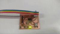
Final Board
Programing Echo Hello Board
So i have my own Echo Hello Board. I'am excited to program and use the board myself. So i'am going to program my Echo Hello Board using my FAB ISP that i made in electronics production week. So first iam going to program the board using Arduino IDE. Then i will go forward with Atmel Studio. So here it goes.
Method One : Programing With Arduino IDE
Arduino is a opensource electronic development platform. Usually we can program most of the AVR microcontroller using Arduino IDE learn more from here.
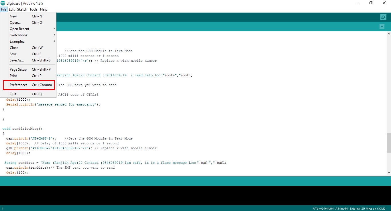
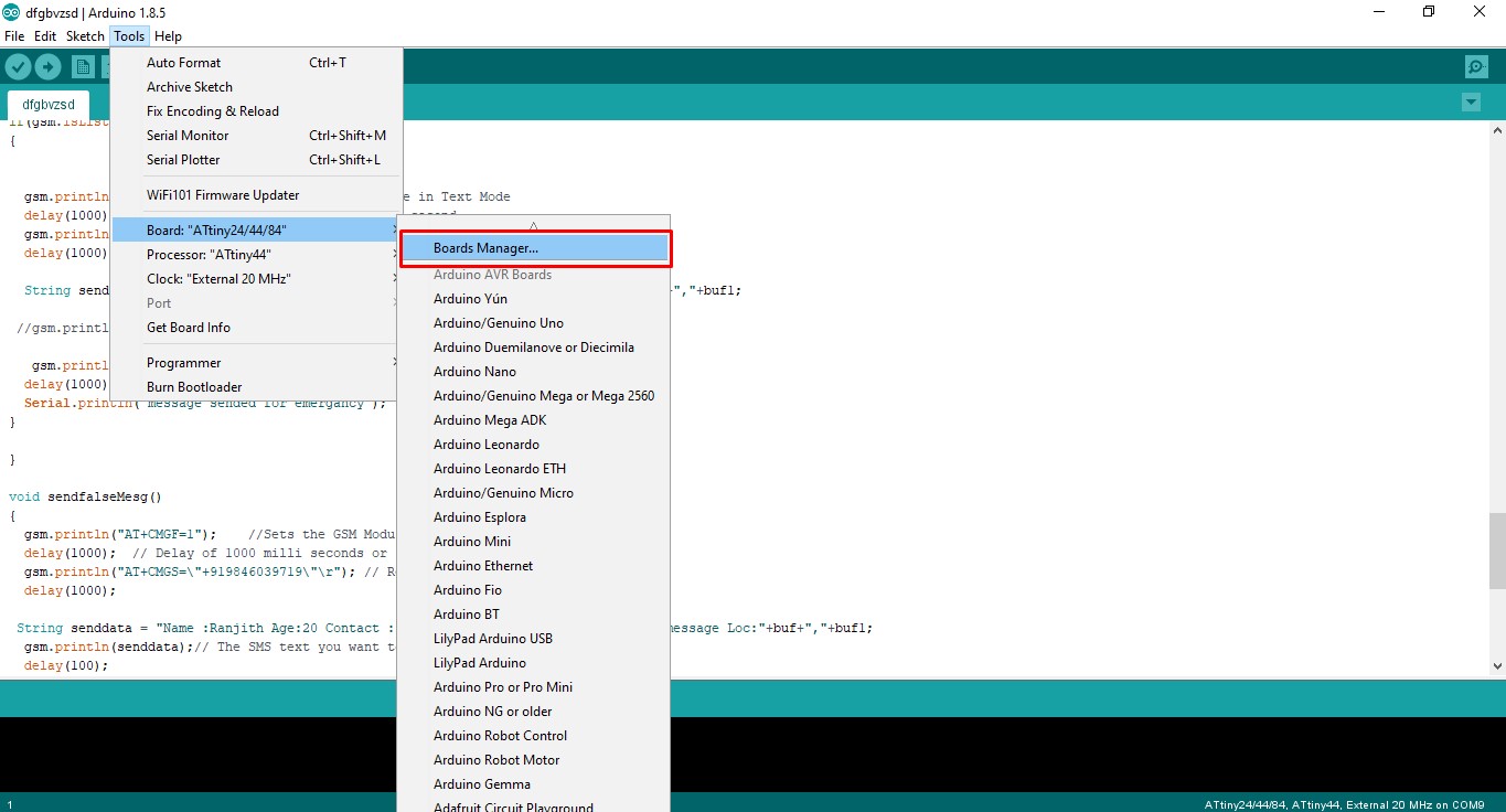
First you need to download and install Arduino IDE fromHere.First I open the arduino IDE. Then I need to Download the necessory board manager files in order to program the Attiny series microcontroller through Arduino IDE. Follow the below steps to install the board manager in your Arduino IDE.
Step One : Copy The Additional Board Manager URL
To apply the Additional Board Manager URL, first You need to Copy paste the Additional Board Manager ULL Below.https://raw.githubusercontent.com/damellis/attiny/ide-1.6.x-boards-manager/package_damellis_attiny_index.json
Then Follow the Below Steps:
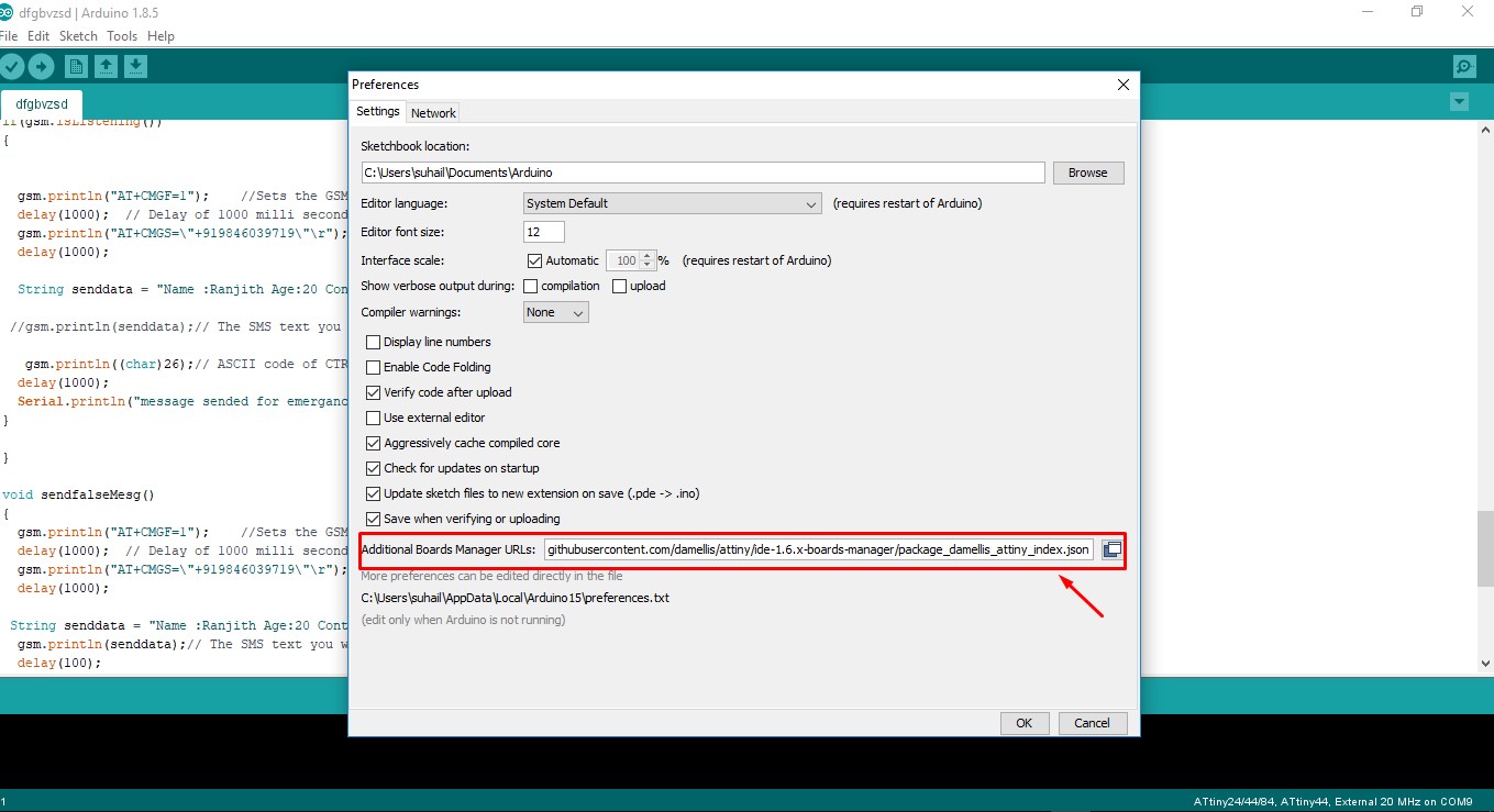
- Go to File -> Prefererance -> Additional Board Manager URL
- Paste the URL in the text field and click ok
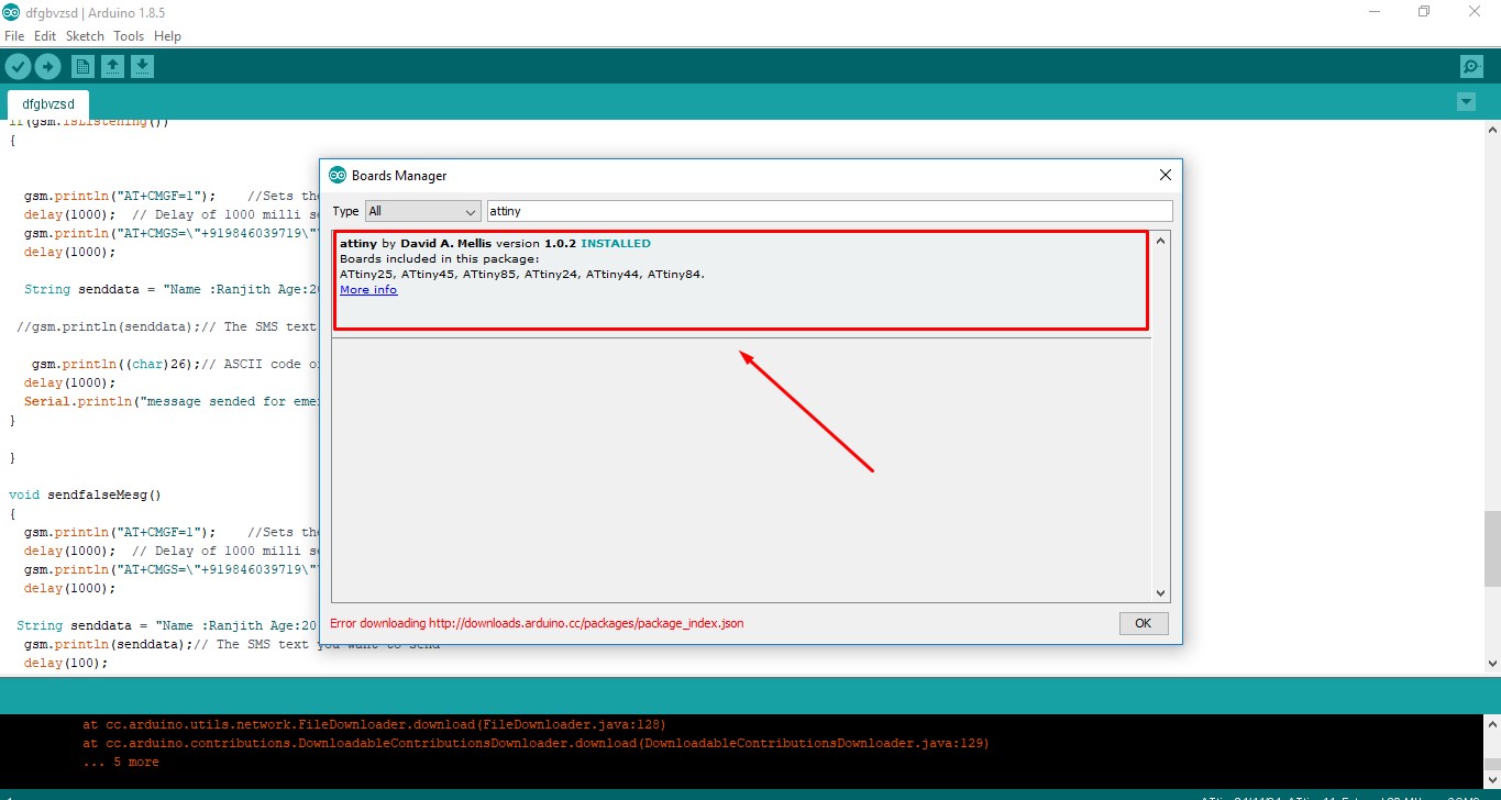
- The go to Tools -> Boards -> Board Manager
- Search for "Attiny"
- Install the board manager for Attiny 44 by david A. mellis
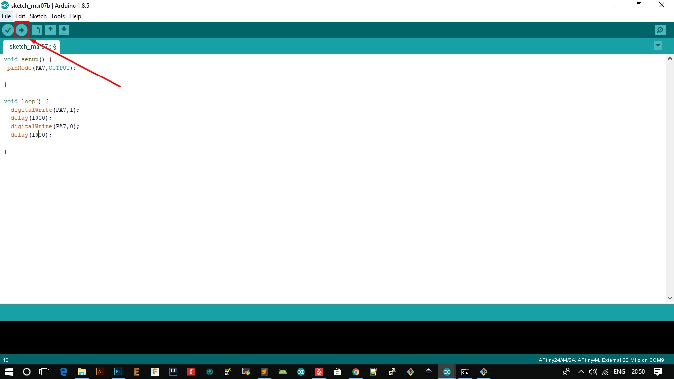
Step Two : Write a Blink LED COde
Now i wrote a simple Blink LED sketch for my Board. I have a Blue LED conected to the Attiny44's PA7 pin. The code is given below:void setup() {
pinMode(PA7,OUTPUT);
}
void loop() {
digitalWrite(PA7,1);
delay(1000);
digitalWrite(PA7,0);
delay(1000);
}After writing the code Upload by clicking the Arrow button on the top left corner of Arduino IDE.
ERROR IN MY PCB
There is remarkable error that i made in PCB. I accidentaly give the LED Anode Pin to vcc that i would need to conect to the PA7 pin. So the led is always lights up. So i redesigned the board immediatly and i updated the resource files too. But we are using the final milling bit left in our LAB. It was broke while in milling of a board. So, We dont have milling bits now. We should need to wait about weeks to arrive the bits. So, what i did is, i cut of the vcc trace to the LED and conect a jumper wire between LED anode pad and PA7 pin of attiny44. It is works well see it below.
OUTPUT
Group Assignment
In this week we need to complete week assignment too. We need use and test the electronics equipment in your lab to observe the operation of a microcontroller circuit board. So we started to test our equipents in our lab. First we madee a basic understanding about the Equipments. SO i explain what i learned from the group assignment.
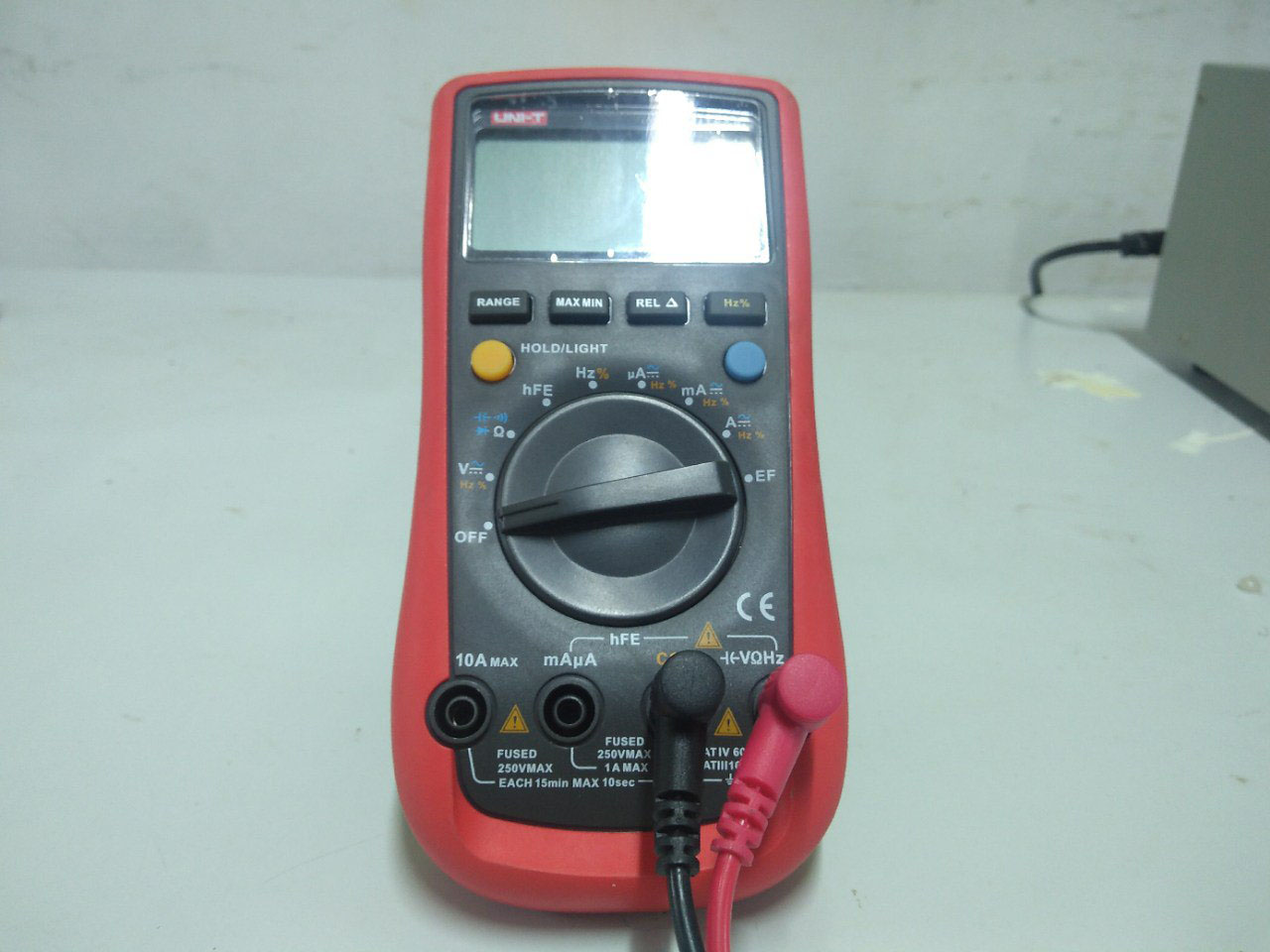
MultiMeter : UNI-T UT61A
Multimeter is the most and primary tool that every electronics enthusuiast needed in their Lab. We have many types of multimeter available in the market. Its depends upon US, wich one we needed. We have a Amprobe PM55A available in our Fablab. Amprobe PM55A is Automatic precision pocket sized multimeter. It is a excellent one. But i use my personal Multimeter because it is more suits for my needs. I use UNI -T UT61A Multimeter. The UT61A is a 4000 counts DMM featuring 41 segment analog bar display and 400Hz bandwidth multimeter. This is not the best one. but its suits my needs. The UNIT - UT 61A is automatic range selection. UT61 series complies with CE, ETL, and GS standards. This series is all auto ranged with seletected True RMS models (UT61 D/E). This series has an abundant of features, combined with high safety rating of C AT IV 600 V. It is suitable for both beginners and advanced electronics, and electrical users.
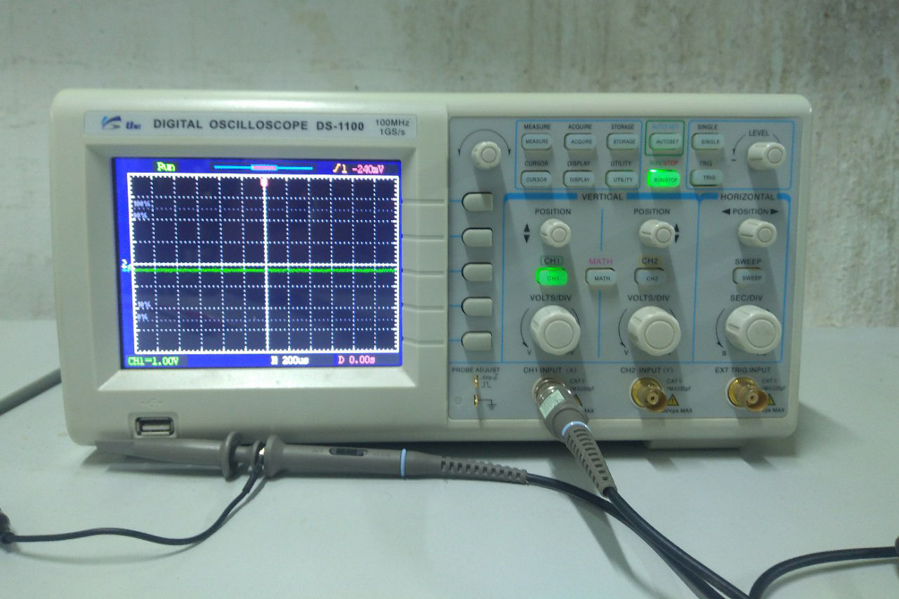
Oscilloscope : UniSource DS-1100 100 MHz
When We are doing singnal based stuffs or input and output devices we always needed a Oscilloscope to test the signals. Oscilloscopes will visualize the data and other information reagrding the signal that we testing. We have a UniSource DS-1100 100 MHz, 2 Channel Digital Storage Oscilloscope in our F 100 MHz bandwidth, 1 M Memory abLab kochi.
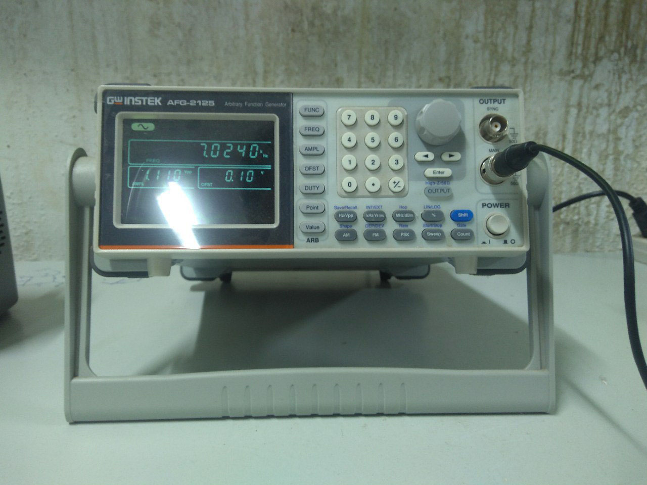
Function Generator : UniSource DS-1100 100 MHz
The AFG-2100/2000 Series Arbitrary Function Generator is a DDS (Direct Digital Synthesized) based signal generato.It can generate output of Sine, Square (Pulse), Ramp (Triangle), Noise and Arbitrary waveforms. It provides 20M Sa/s sampling rate, 10 bit vertical resolution and 4k point memory .Also it can generate 0.1Hz resolution of Sine, Square and Triangle waveforms and the 1% ~ 99% adjustable duty cycle of Square (Pulse) waveform We can conect our devices that we needed to test with the probes of the function generator. It should help us to decide both the output and input devices signal range and voltages etc...
Function Generator : UniSource DS-1100 100 MHz
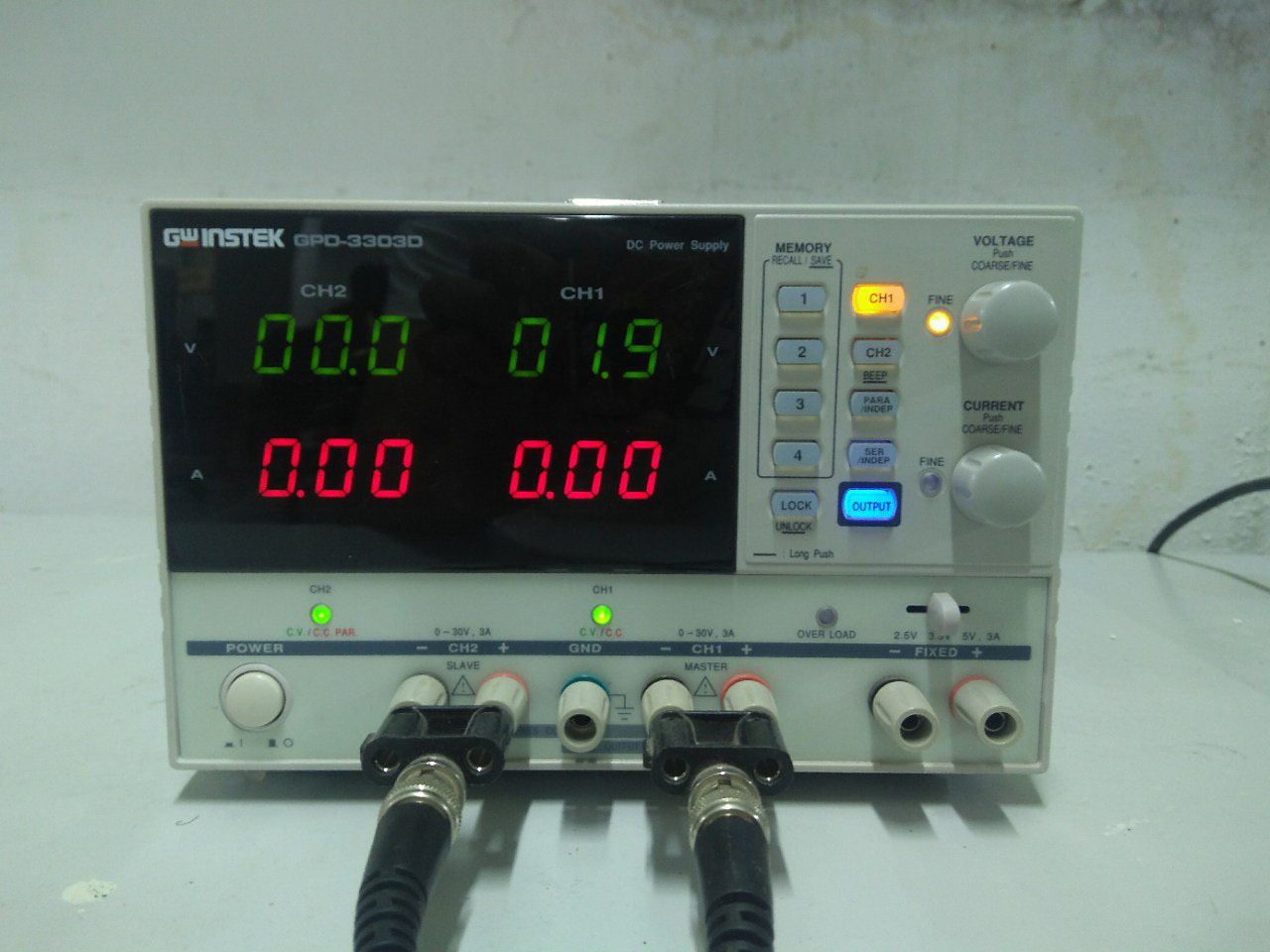
If we are making some cool electronics stuff or even we need to power a circuit. We always need a bench power supply that have a adjustable power supply features. We always need Bench power supply in our lab. The Instek GPD-3303D 3-Channel Programmable Linear DC Power Supply, 195W, 100mV/10mA is a good bench power supply that we had in our Fablab Kochi. I used the bench power supply to test my LED is working or not by powering the Board. It works well.