TODO LIST
- Make an ISP with the help of PCB Milling Machine
Introduction
The Fifth-week assignment is to learn about PCB fabrication and milling. I need to mill a Fab ISP (In - System - Programmer) by using Modela PCB milling machine. I have experience in Electronics and PCB designing. I never used a PCB milling machine much before. But i used an assembled opensource Milling mechine . I usually fabricated my PCBs using toner transfer method. In some case, it was so easy but the most case it is time taking and expensive when comparing with PCB milling machine. In fab Lab, we have a modela PCB milling machine. My primary goal is to learn and use Modella PCB milling machine and make a Fab ISP.
PCB fabrication
PCB ( printed circuit board ) fabrication is the assembly technique for circuit boards used in electronic devices. The layers of the board stuff together in a specific surface pattern. The conductive traces are physically connected together according to the circuit. The PCB made out of a base layer and conductive layers. The re-enforcement base is commonly made out of glass or epoxy. They are highly heat resistant. The conductive layers are made out of copper. Copper is the most commonly used conductive layer for PCBs. PCBs come in both single sided and double sided. But in manufacturing level we have multiple layers like 3 or 4 layer PCBs
Eg :: Motherboards are commonly made out of 4Layer PCBs.
Different Prototype PCB fabrication Methods:
- Screen printing
- Toner transfer method
- Dry film tranfer method
- PCB milling
PCB milling Mechine
PCB milling mechine is a CNC (Computer Numerical Control) machine that used to fabricate rapid PCB prototypes . PCB milling mechines are mill away the copper parts of the copper clad to make out traces and pads of the PCB. The PCB milling mechine is comes with a three axis mechanical movement (X,Y,Z) . Each axis are controlled by stepper motor for precisional movements. These axis movements are controlled by a computer program by giving Gcode commands. Gcode is a widely using Numerical control programming languages, most machines are using gcode to control the axis of the mschines. A tool head (usially a milling bit) is conected to these axis will mill out the PCBs. We have a Modela MDX20 Machine at fablab kochi.
Modela MDX20
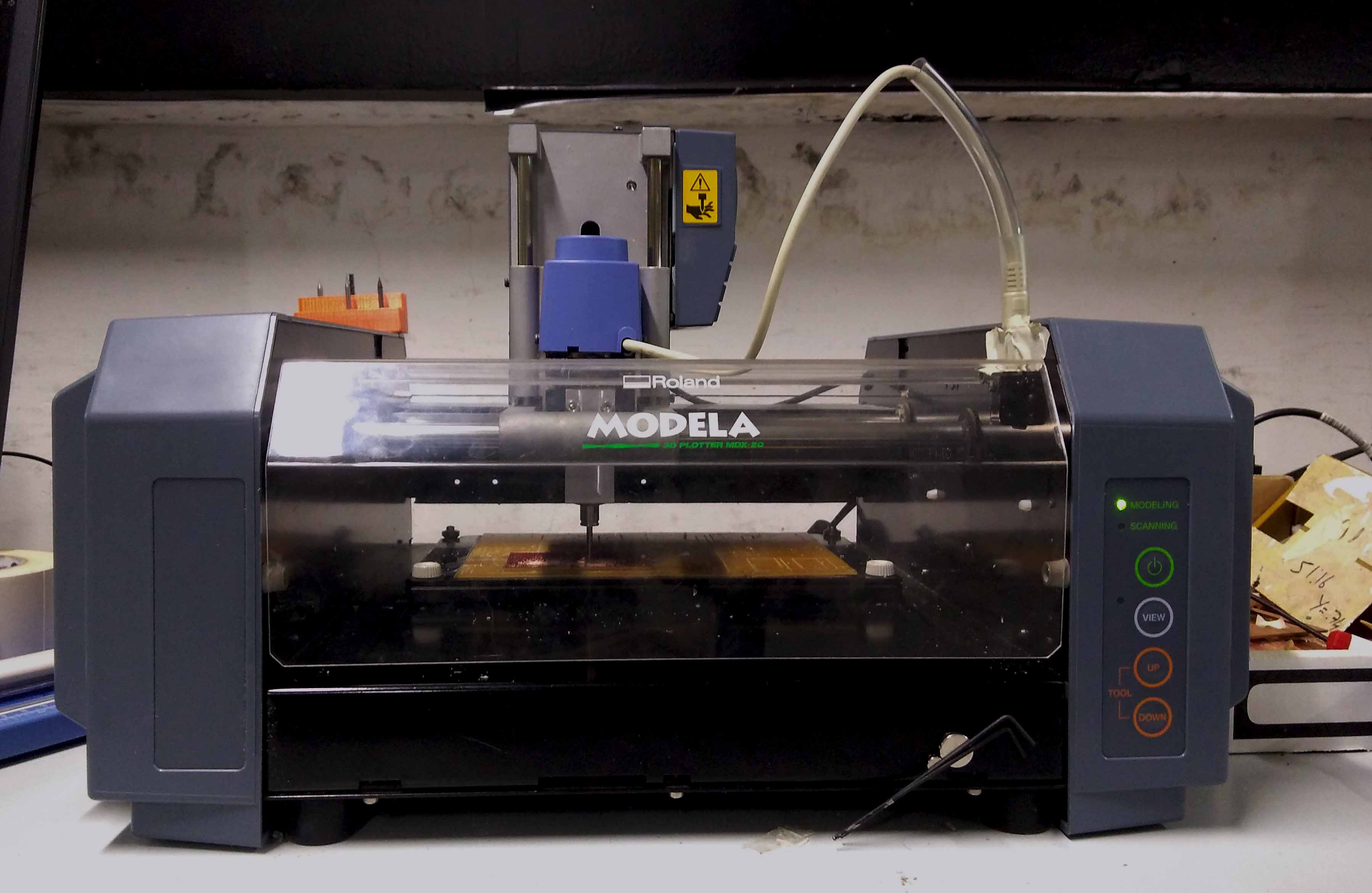
Modela MDX20 is PCB milling machine. Modela MDX20 is usually used to fabricate PCBs but we can also make moldsings, etchings etc... Modela can mill on different materials like Plywood, Wax, Acrylic, Differents PCB materials like Fr1 Fr4 etc... The modela is light weight and comes with small in size. We can place it on even a small desktop. The bed (milling surface) is attached to Y axis and the tool head is attached to X and Z. That means the movement of bed is controled by Y axis and movement of tool head is controled my X axis and the height of tool head is controled by Z axis. Modela have its own computer program. But we use Fab Modules to communicate with Modela to control the cutting and milling process . Fab Modules never set X,Y,Z axis automatically, we need to set them manually. It is more precisefull.
Get started with Modela MDX20
If i wan't to mill my PCB, in this case a FabISP programmer. First I need a PCB design layout and a PCB outline layout. The PCB milling is a two stage process. In first stage, i need to mill out the traces and pads of the PCB and in the second stage i need to cut out the PCB outline.
Using fab modules we can convert .png PCB design layout to G-code. The G-code contains the coordinations and tool path to mill the PCB. The .png image should be in black and white color combination. The milling machine will mill out the white portions using the tool head and the black portions will leave without mill. So, the traces and pads should be in black color format.
General overview
- Workspace : 203.2 x 152.4 mm
- Z axix stroke : 60.5mm
- Spindle speed : 6500RPM
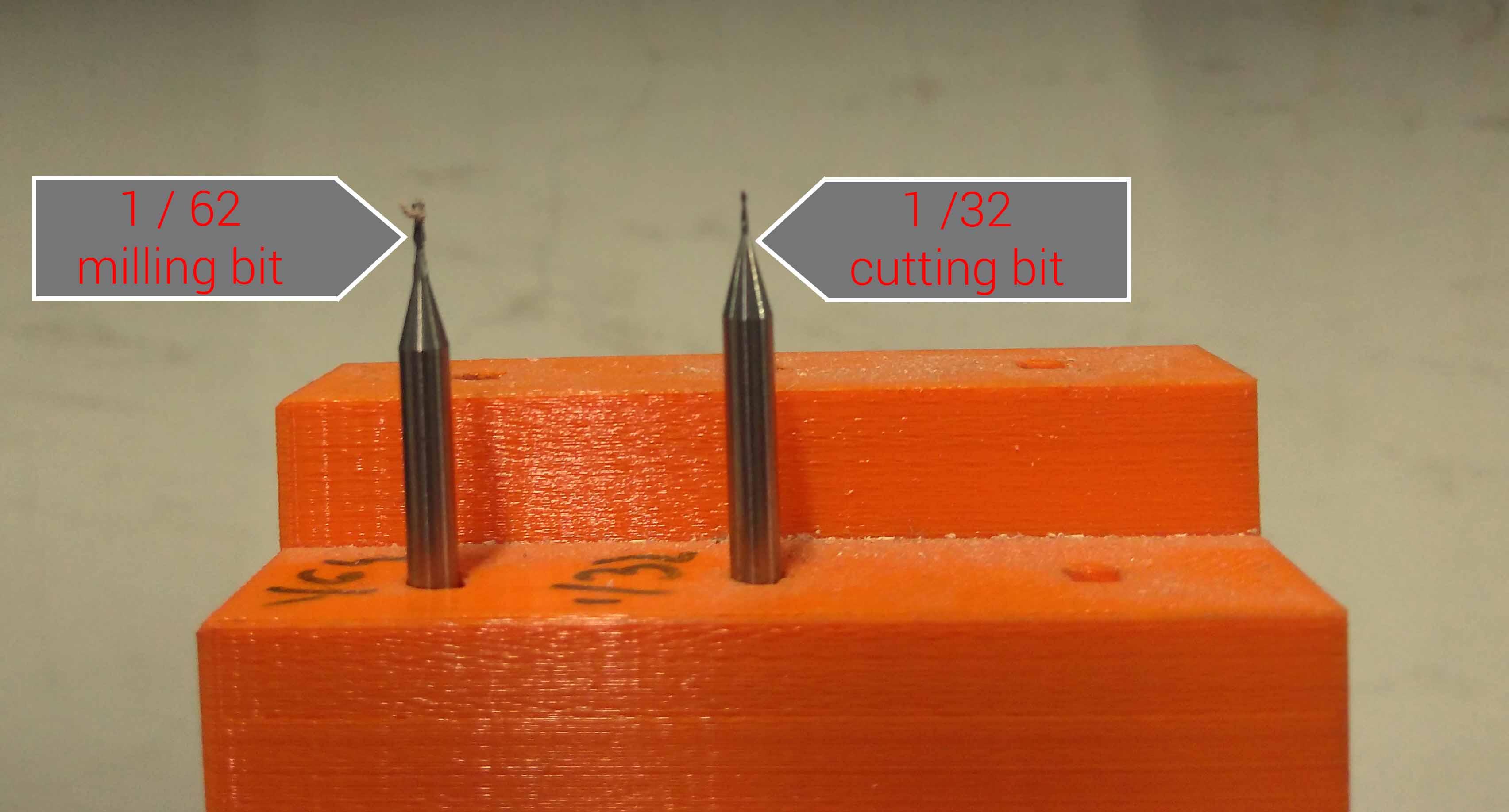
Milling Bits To use
- Milling Bit : 1/64 inch (0.4 mm) bit
- Cutting Bit : 1/32 inch (0.8 mm) bit
What IS ISP (In - System - Programmer)
In System Programmer (ISP) also known as In Circuit Serial programmer (ICSP) is a microcontroller programmer. The ISP will read the instructions and commands from the computer USB and send to the Microcontroller through the serial peripheral interface (SPI). Simply ISP devices allow us to communicate with microcontroller using SPI lines. SPI is the way of communication in microcontroller. Every conected peripherals and interfaces are communicate with microcontrollers through SPI. As a electronic enthusiast, the first thing comes to my mind when say about ISP is MISO, MOSI SCK .
These three pin are the important pins.
ICSP pin Diagram
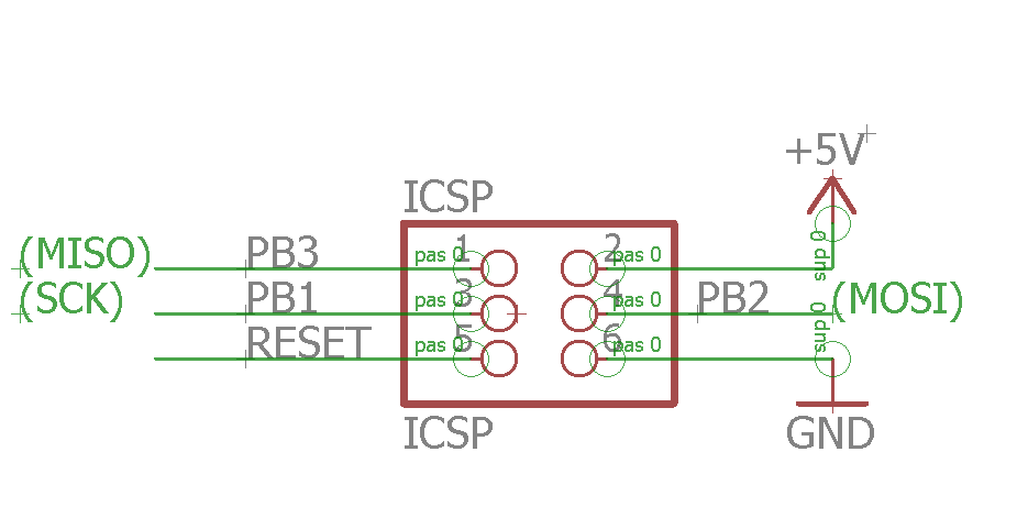
ICSP pin diagram
Fabricating FabTinyISP
FabISP is availabe in two versions. The original FabISP by Neil Gershenfeild and FabTinyISP contributed by many peoples. The ATtiny44 is the microcontroller usid in FabISP and the Attiny45 is used in FabTinyISP. I decided to use FabTinyISP because it is small in size. I used this Documentation to get all resources to make one by myself.
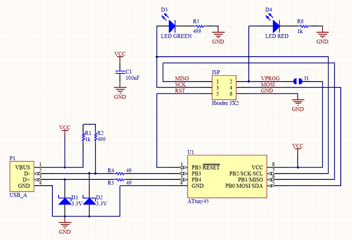
FabTinyISP Circuit Diagram
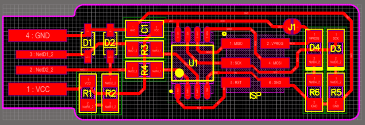
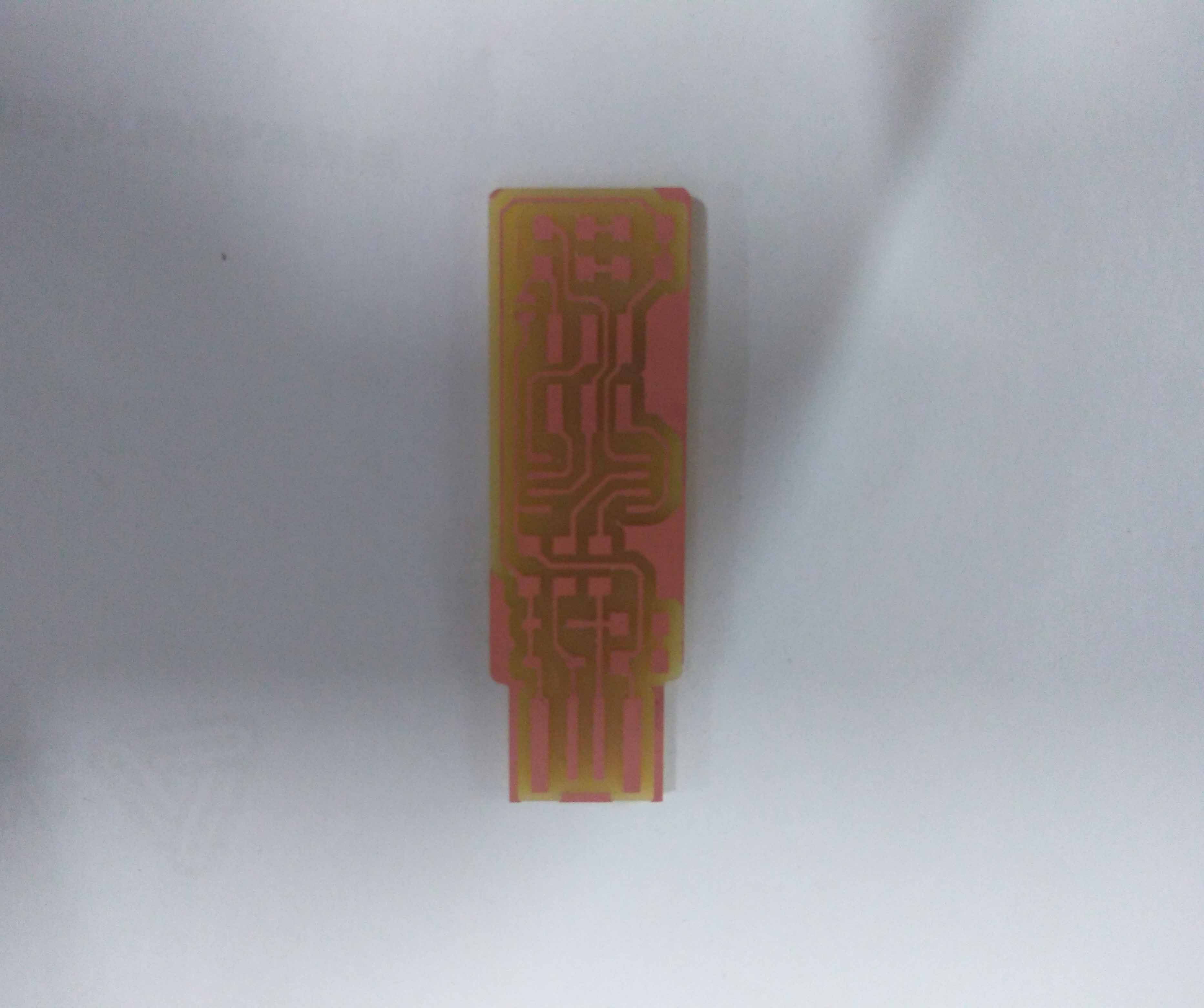
FabTinyISP PCB Overall Layout
ATtiny 45 Microcontroller
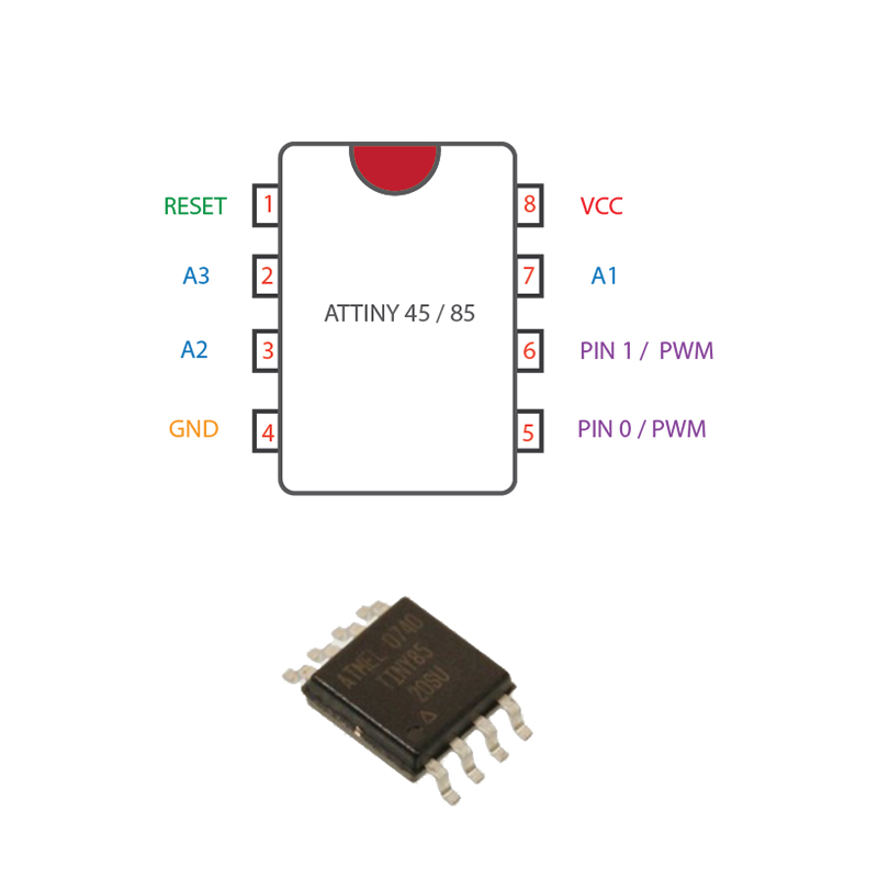
The microcontroller that is using in FabTinyISP is Attiny 45. Attiny45 is a High perfomance and low power 8- bit AVR microcontroller running on RISC Architecture by Atmel (microchip acqured Atmel recently). Attiny 45 comes in a 8 pin package. Attiny 45 have 6 I/O pins, Three of them are ADC pins (10 bit ADC) and other two are Digital pins supporting PWM.It comes with a 4KM flash memory, 256 In-System Programmable EEPROM and 256B SRAM. Operating voltage around 1.8V to 5.5v 300mA. Attiny 45 support Universal Serial Interface. Both SMD version and THT versions are available in the market. Attiny 85 is a higher version of Attiny 45, They are almost same. Tghe only difference is in the Flash memory, Attiny 45 have 4KB flash and Attiny 85 have 8KB flash. We can choose either Attiny 45 or Attiny 85, Not a big deal but Attiny 45 is more enough to make FabTinyISP. In fablab we have SMD version of Attiny 45 is available. See the official documentation from here.
- ATtiny 45 : 4KB FLASH /256 B EEPROM / 256 B SRAM
- ATtiny 85 : 8KB FLASH / 512B EEPROM / 512 B SRAM
Special Features :-
Setting Up Machine
In the previous section, i simply explained about PCB milling machine and model MDX20. In this part i need to setup the modela MDX20 to mill my PCB. I alreday said about milling bits and computer program to send instructions to the mechine. Here i explain the way i configured to mill my PCB.
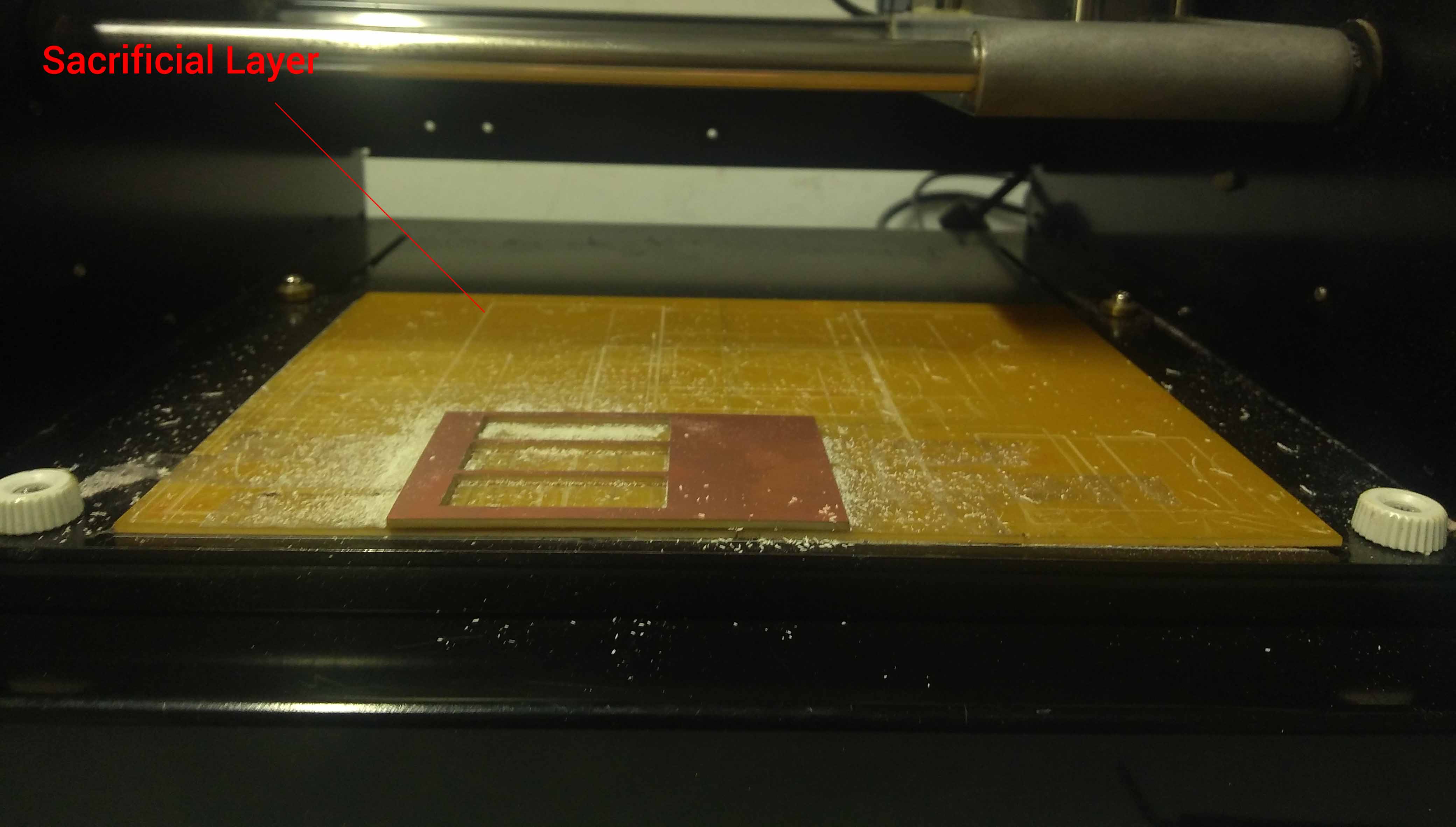
Step 1: Sacrificial layer
First of all, the work plate of the PCB milling machine (AKA milling bed) is a metal plate. It is sturdy and well build. But in some case it may damage while cutting in over depth by mistake. So at fablab kochi we place a sacrficial layer on top of the milling bed (a copper clad placed on top of milling bed to avoid touching bits in the plate). A copper clad sheet is used as a sacrificial layer.
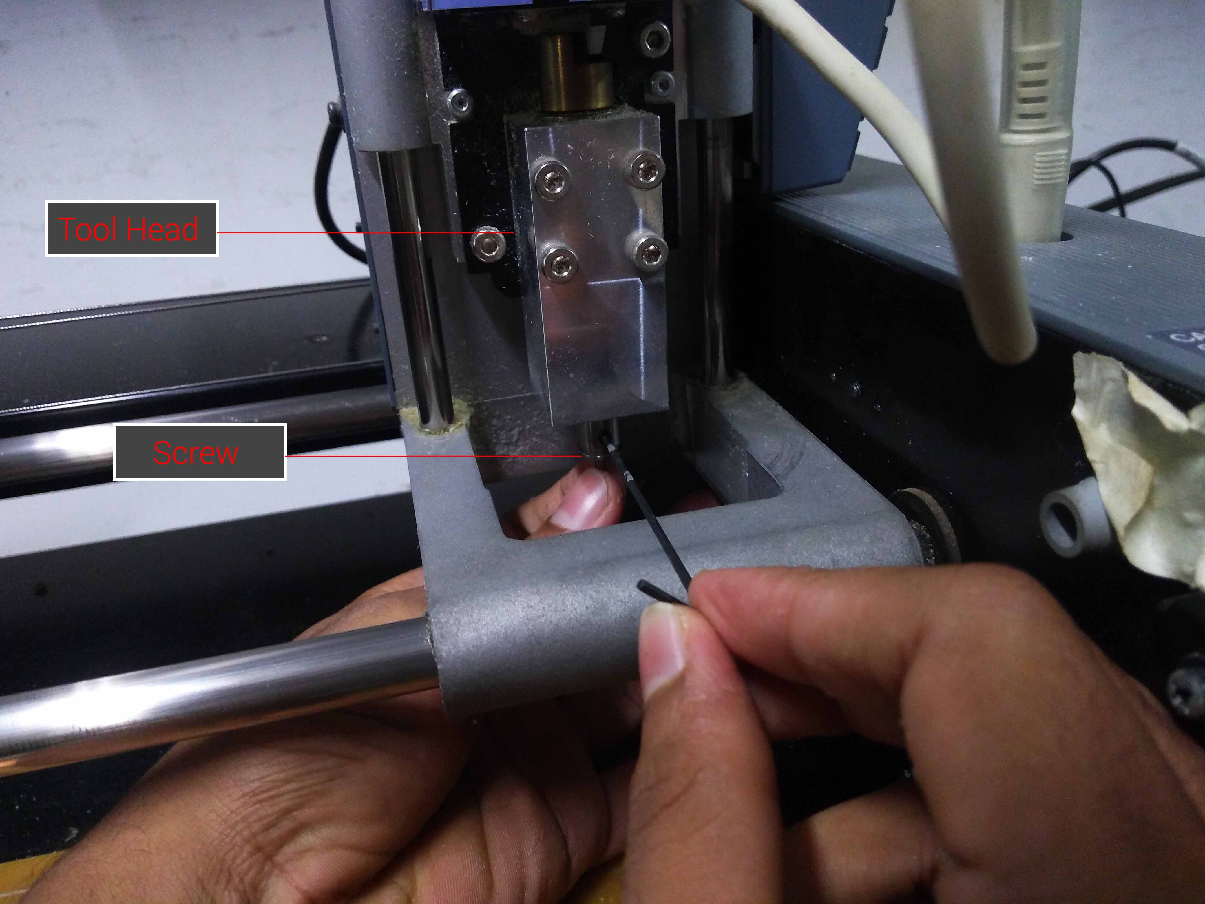
Step 2: Fix the 1/62 milling bit in the tool head
After placing the sacrificial layer, Now i need to fix the milling bit (usually used a 1/62 milling bit) in the tool head. I alreday explained the two stage process of milling PCB in PCB milling machines. First i need to mill the traces and pads of the PCB, thats why i changed the fixed the milling bit first. While cchanging the bits, always give extra care to the bits. The bit's tips are so thin. It have more chances to break the bit while slip from our hands even it is a small fall. to over come this situations i placed a small piece of foam under the tool head to protect from the accidental falls
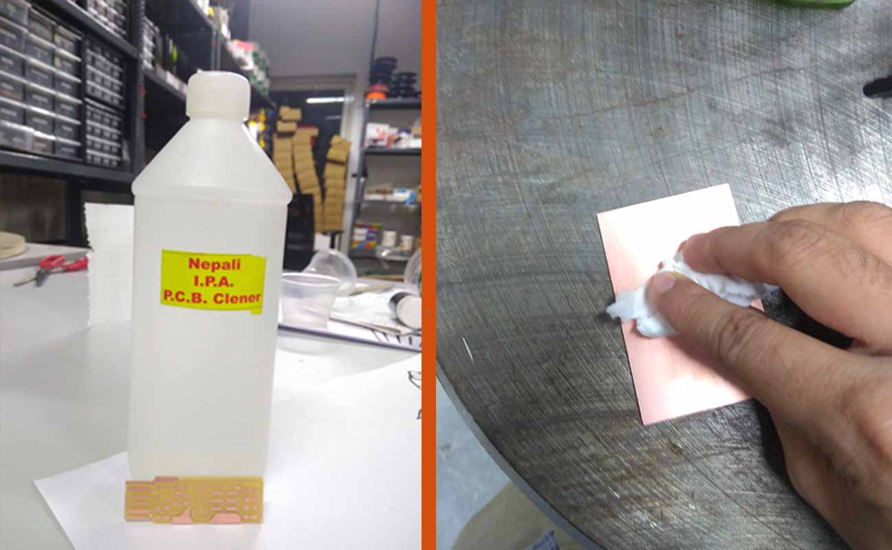
Step 3: Clean the copper clad
We have FR-1 type copper clads at Fablab kochi. The FR-1 are heat resistant and more durable. But copper clads will oxidize quickly and the copper profile are finger print magnets. So before using a copper clad even it is a new one, i recomend you to clean the PCB with a PCB cleaner or acetone before and after milling the PCB. I used a PCB cleaner to clean the PCB.
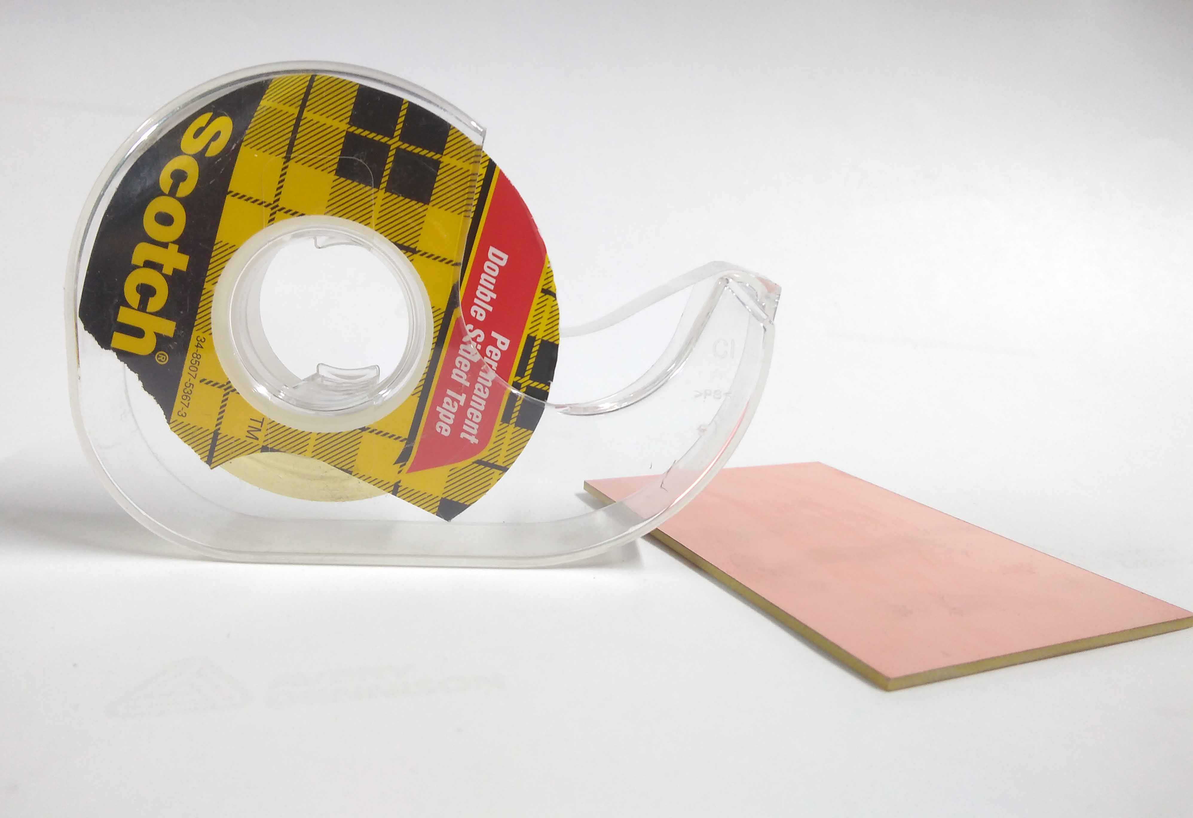
Step 4: Fix the Copper clad on the milling pad
After cleaning the copper clad. Now i should need to place the copper clad on the top of the milling pad. I placed the copper clad on the milling pad with the help of a double sided sticky tape. double sided sticky tap are easy to remove and they are available in cheap price. I stick the doble sided tape on the top of the sacrificial layer. Then placed the copper clad on the top of the ticky tape.
Step 5:Fab modules and PCB milling
I powered on the mechine and then open the Fab module software in a linux system (i'am using Ubuntu) by typing fab in the linux terminal. I got a new window on my screen. I selected image(.png) as my input file format and output format as Roland MDX-20 mill(rml). After that i clicked the Make_png_rml button.
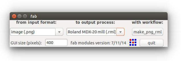
Now a new window will appear. Before further do, we need a PCB trace layout and PCB cut layout. They are given below.
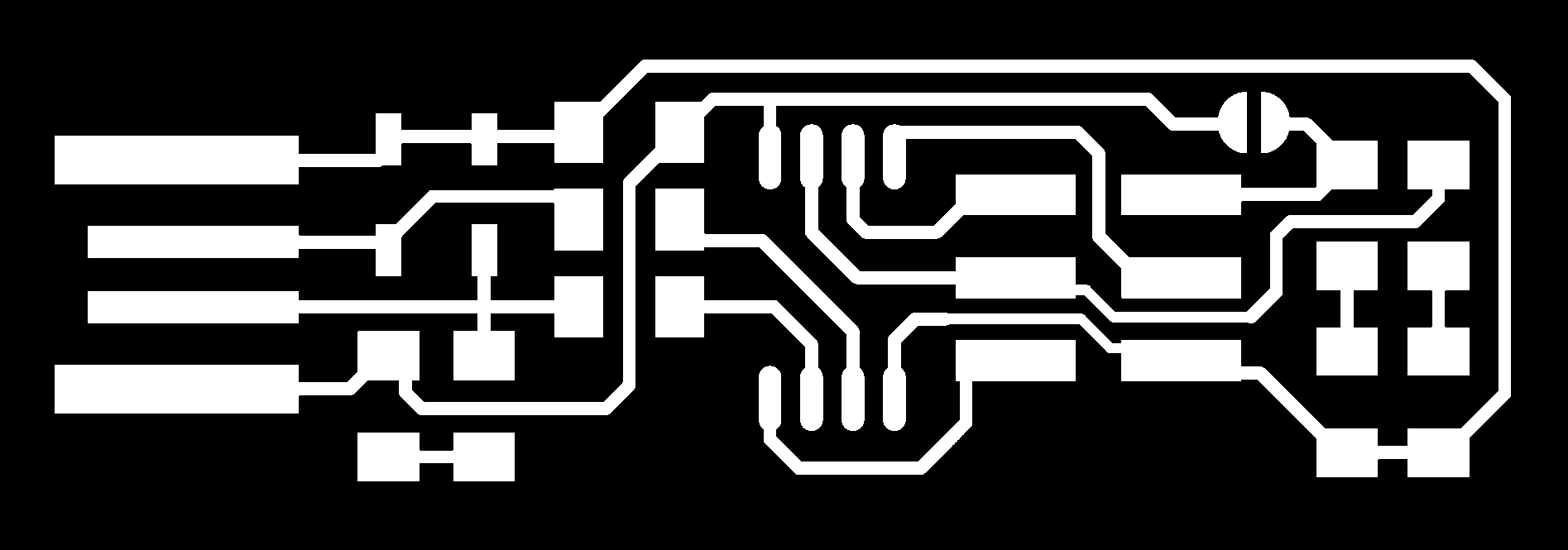

In the top of the new window select the bit that you are going to use. i'am going to use a trace bit 1/62 bit. then load your png format by clink Load.png button. Then click on Make.path button to generate the path to mill.
Now click the Make.rml to generate the instructions and commands for the mechine. You should get a new Send it button on the top make the Make.rml button. Do not click on the button now.
We are not done yet. Now press the View button on the Modela MDX20. Confirm the bit is well tight. press once more the view button to get back to the default position. Now set the X ,Y postions by enetering the messurements (depends on your board position) in desired text boxs. I recomend you to note down the X & Y postions somewhere. If something went wrong and you need to start from first, You shoul need the exact X7Y positions to continue your milling process else it will messup.
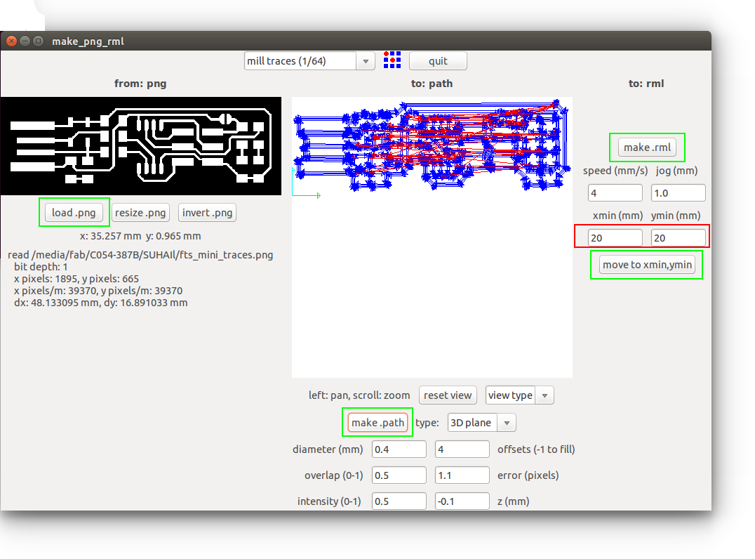
Now set the X axis. Bring down the tool head by pressing Down button. When the Tool head reaches near to the copper clad. press View button and lose the tool head screw and bring down the bit little until it touches the copper layer of the copper clad. then tighten the screw and bring back the tool head to home position by pressing View button. Now we all set. Close the safetly Lid of the Modela and click Send it button. The modela will start to mill the PCB.
It should take a minimum of 10 to 13 minute to mill the traces and pads. after finishing the milling i got a good result.
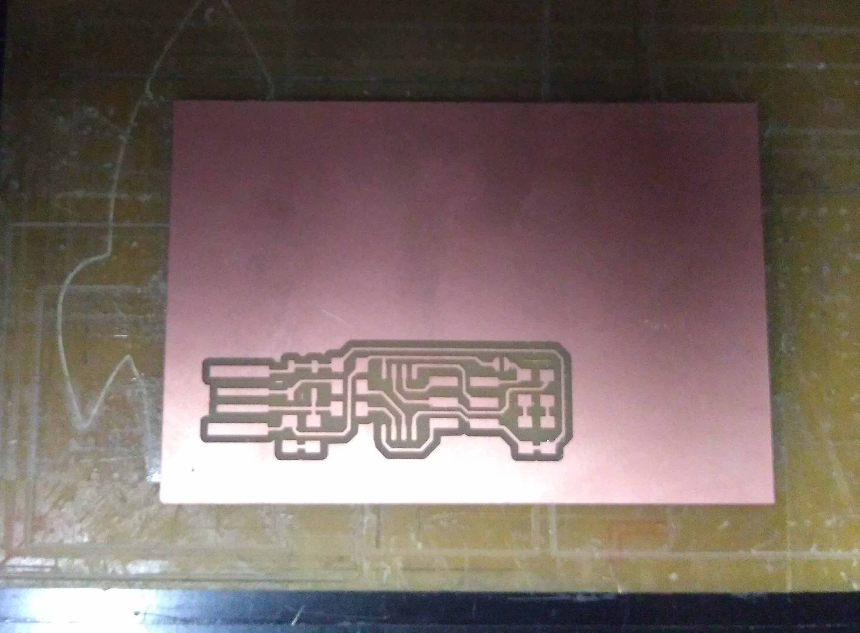
Step 5:Cutting Outline layout
After finishing the Trace milling. Now i need to cut out the PCB outline layout(simply shape of the PCB). The process is almost same. For cutting the layout. We should use 1/32 bit. change the milling bit to cutting bit. Then load the cutting layout png file to fab modules. Then i countinued the same procedures that i followed in the last step. after cutting the cut layout. it should look like this.
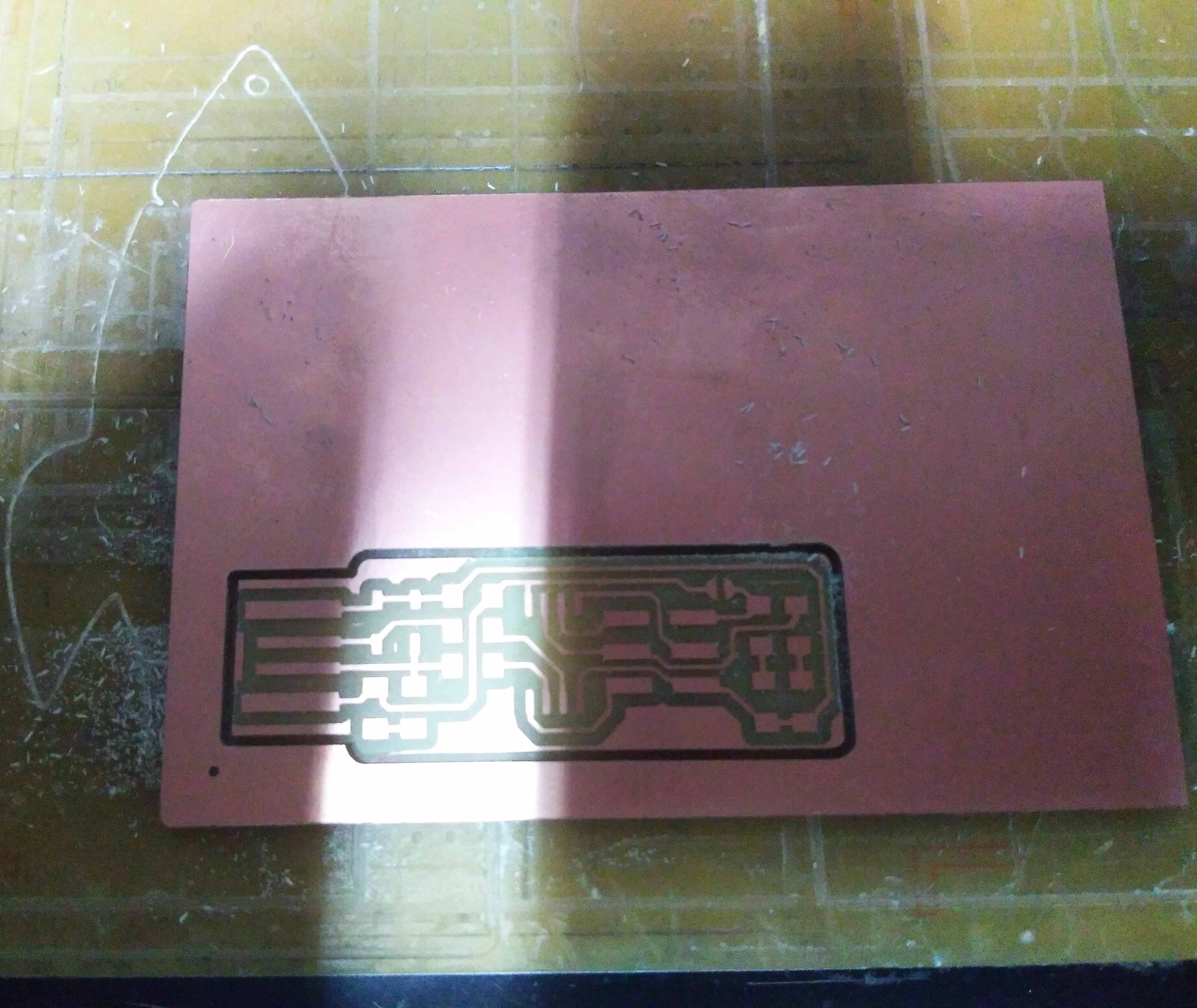
Finishing PCB Milling Process
I sucessfully milled my FabTisnyISP PCB using Modela MDX20. I carefully removed the copper clad from the sacrificial layer and cleanedthe dusts in milling bed using a dust buster. Then i cleaned the PCB one again using the PCB cleaner.
Fun Part: Soldering Components on PCB
Now i have a finished PCB. all i need to do is solder all componets on the PCB. For me, it is fun and easy task. First i need to collect all the componets and grap the tools needed to solder.
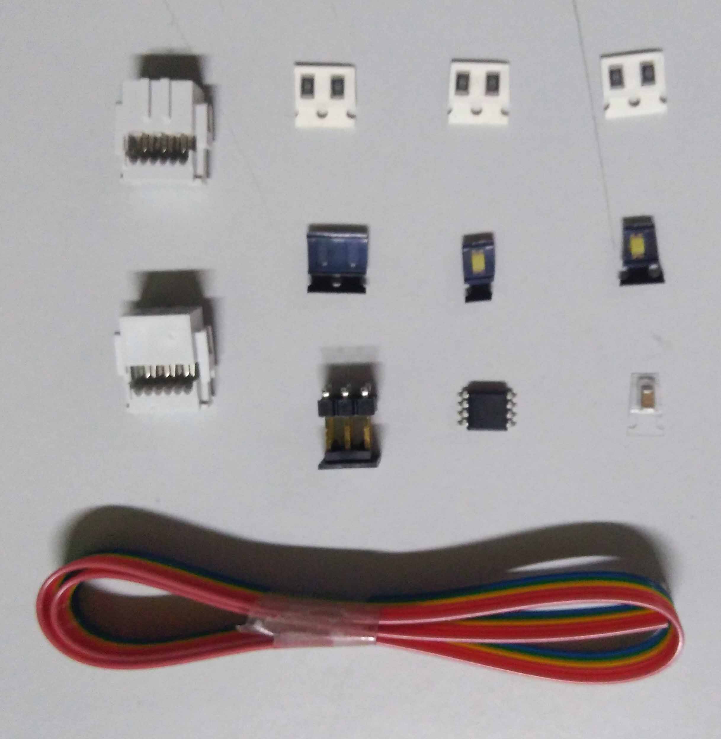
Components list
- 1 x Attiny 45
- 2 x 499 Ohms
- 2 x 49 Ohms
- 2 x 1K
- 2 x 3.3 zenor diode
- 1 x 0.1mf capacitor
- 1 x Blue led
- 1 x Green led
- 1 x 2x3 Male header pins (smd)
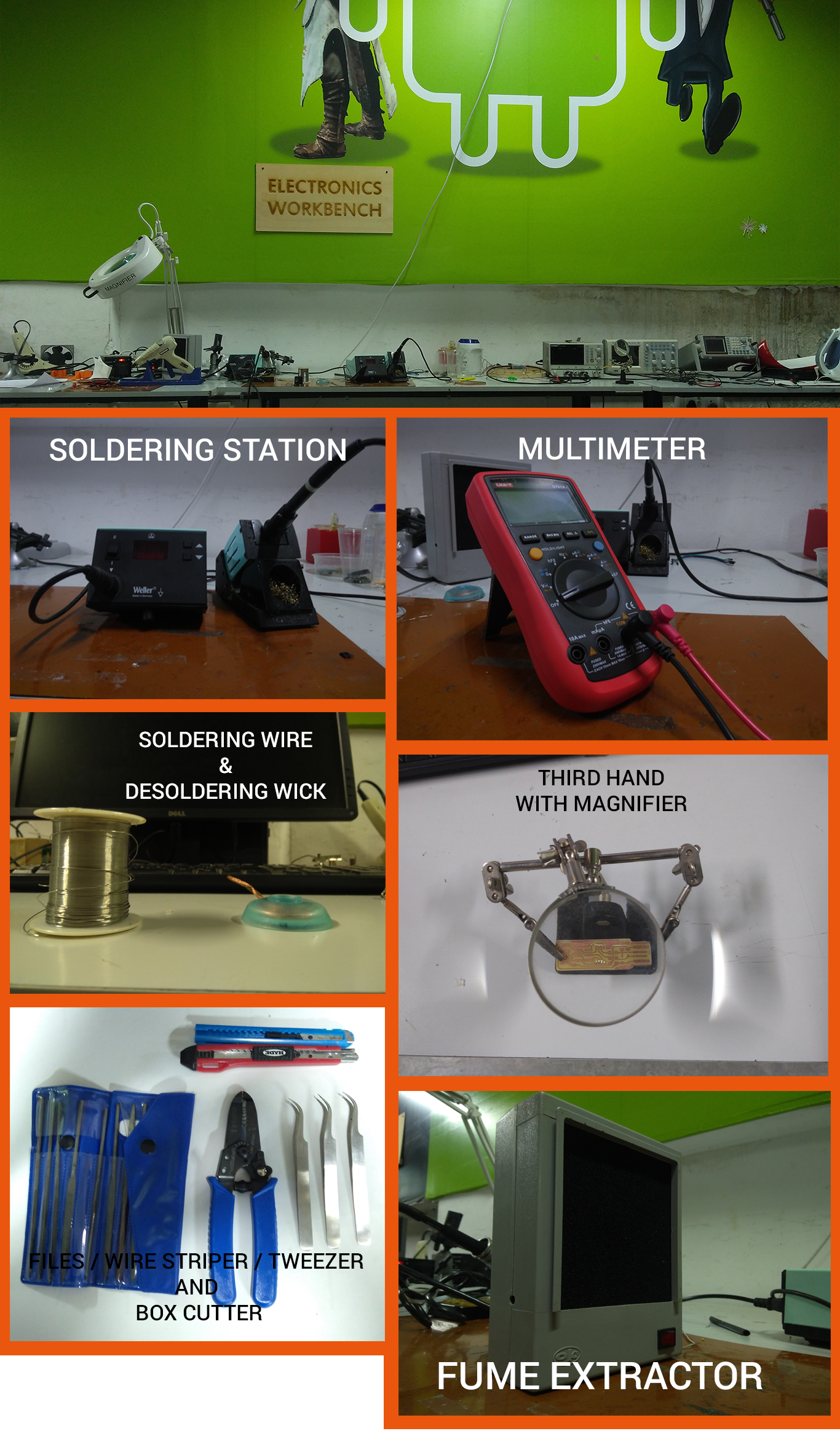
Tools requrements
- Weller soldering station (Micro tip)
- Soldering Lead wire
- Tweezer (micro tip)
- De soldering Wick
- Magnifier
- Multimeter
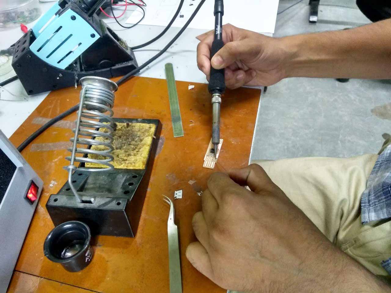
Soldering Componets
When it comes to soldering. Through hole components are so easy to solder when comparing with SMD components. SMD componets are small in their footprints. it will leads to difficult to solder. there are a lot of chances to make mistakes like cold solders misplacements of compoents and most common thing making bridges and shorts in between traces. But everyone have their own soldering tips and tricks that learned from their own expeirience. this will make this task fun and easy.
How I soldered My FabTinyISP
I have experience in soldering SMD before. I usually solder Microcontrollers and Other ICS first. Then i solder small components like resistors and capacitors etc... At last through hole components, wires and header pins. To older my FabTinyISP, i follow the same steps. To solder SMDs easly, First i heatup the soldering iron around a 350°C. Then add some solder flux on pads. Then i well heatup the pad wich i want to solder components, then i add little amount of solder to a single pad of the compenent to be placed. Using teaser pluck the component and place it on the pad and heatup the pad for 4 - 6 second. After that solder the other pad. If i make bridges between pins and traces or gives a lot of solder to a component. I used solder wick wire to remove the unwanted solder. I continue the same steps until the PCB fully soldered without any problem. If something went wrong, first i carefully check all traces and components having breaks or bridges using a maginifeir and multimeter.
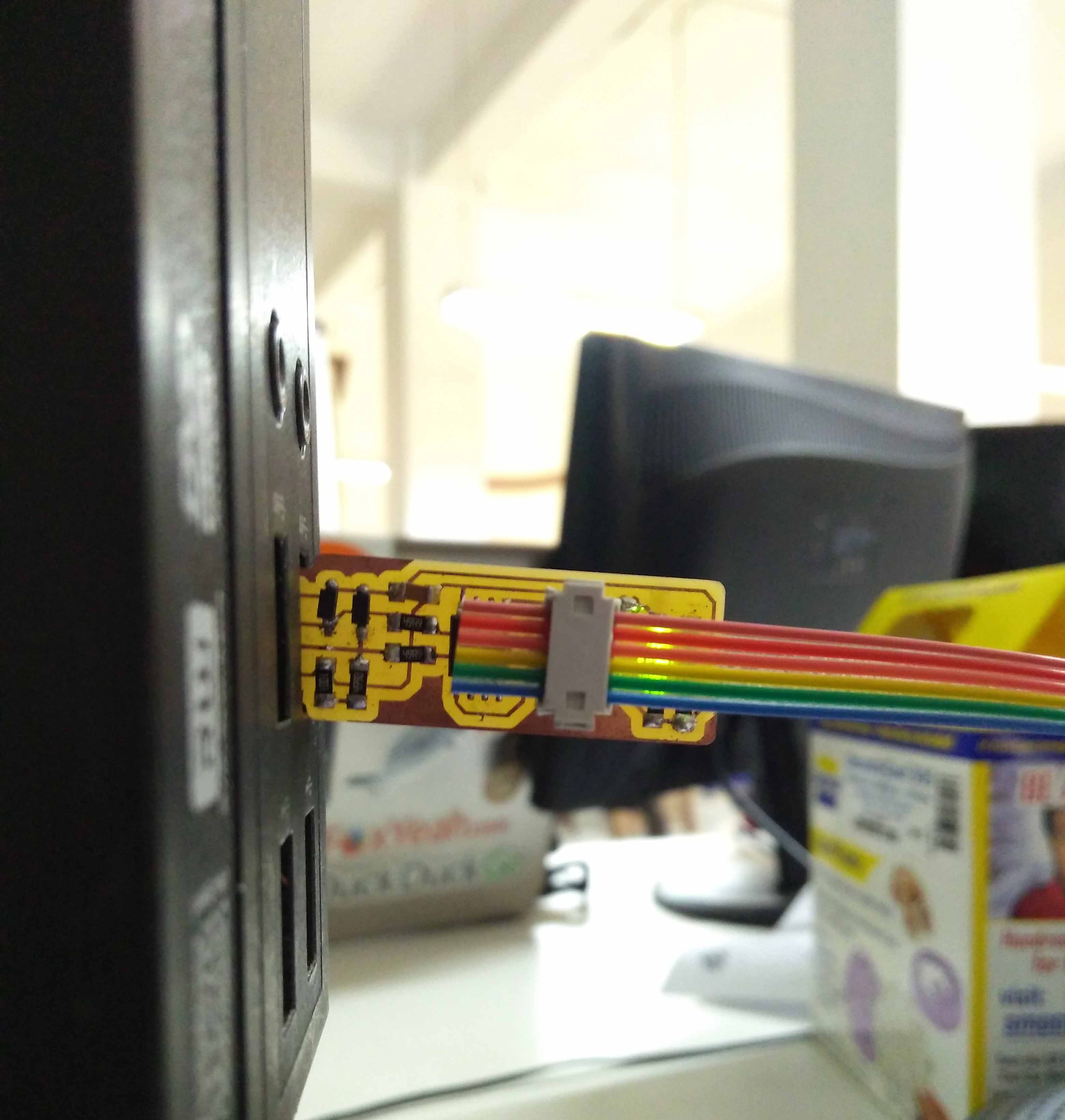
Making ISP wire conector
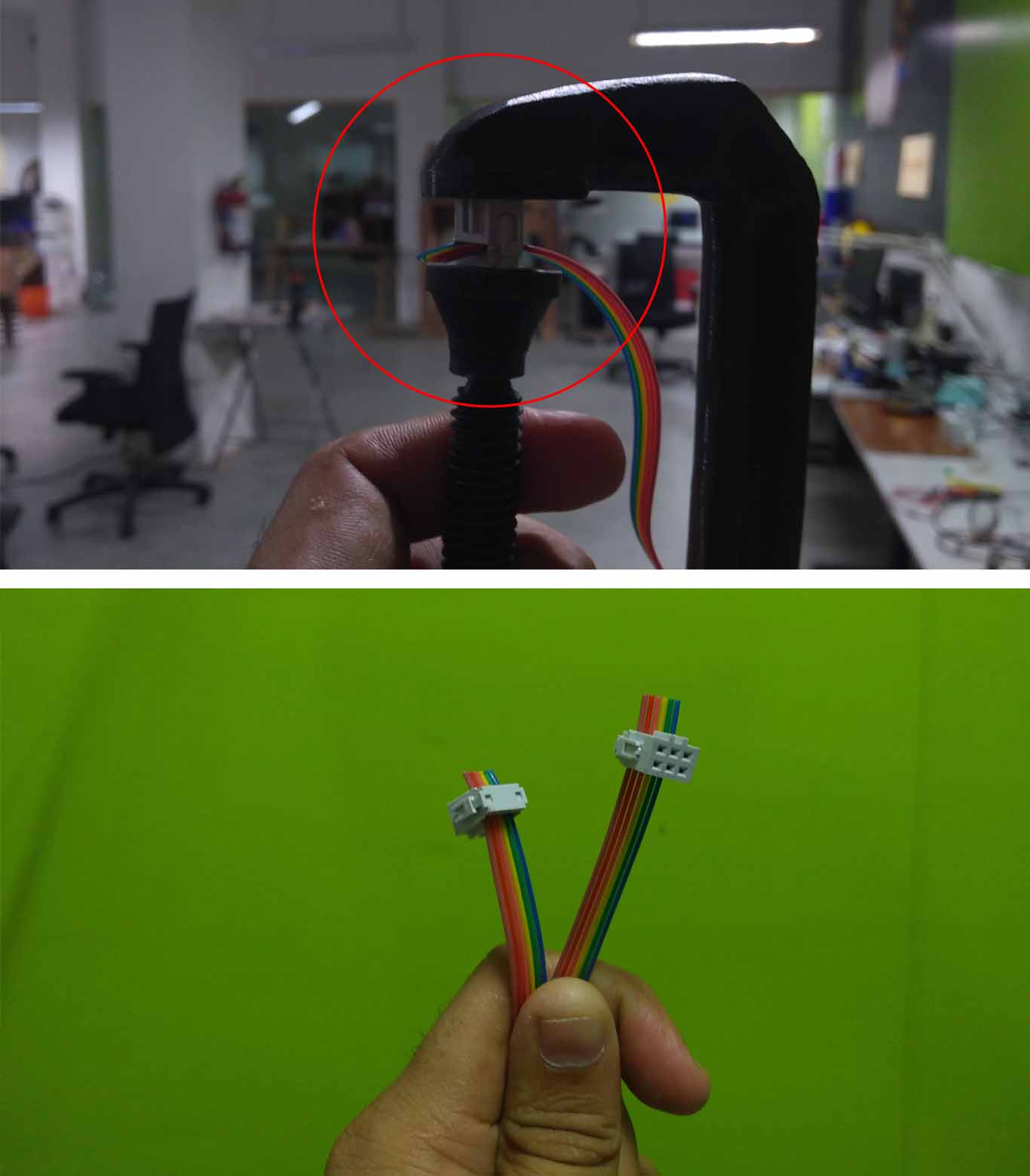
To conect the micr0-controller or another ISP programer to flash the firmwares. we need a six line ribon ribon wire with two 2x3 female wire conector. I used a 4/3 feet 6 chanel ribon wire and carefully conected the female header on both side. To do nicely i used a G clamp. see the below picture
Flashing Firmware
Soldering components to the PCB is not the final step. Now i need to flash the firmware for the ISP. The firmware is opensource (technically FabtinyISP is opensource). I doesn't need to write the code. Just i need to flash it to my FabTinyISP board. To do that Fist i need another FabISP or FabTinyISP to flash the firmware to my bareborn Attiny 45. We have aFabTiny ISP here that is made by a student last year. I use a linux sytem to flash the firmware. So , lets get started.
Step 1: Install AVR GCC tool chain
First of all, we need to install the tool chain. To do that, open a Linux terminal and type
sudo apt-get install avrdude gcc-avr avr-libc make
Step 2: Download and unzip the firmware
Now i need to download and unzip the firmware files. You can download it from here. After download the zip file, Unzip it in a good location that you can find easly (to avoid necessory confusions).
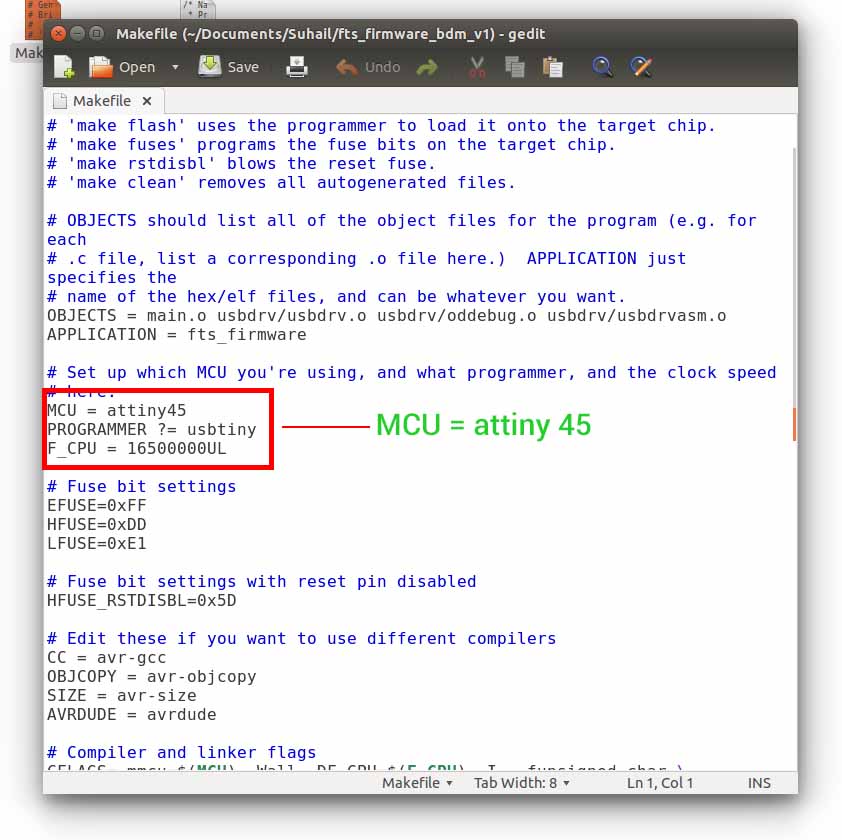
Step 3: Make file
Before burning the firmware. we need to enssure the makefile is configured for the Attiny microcontrollers. To do that open the Makefile in any text editor. then confirm MCU = Attiny45. See the image below.
Step 4: Flash the firmware
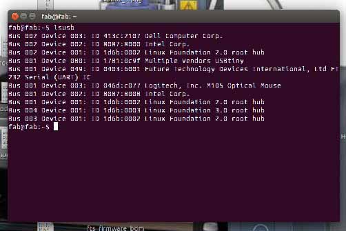
Now we can flash the firmware to our ISP. To do that we need an another ISP programmer. I used a FabTinyISP that made by a student in the last year. I conected both the ISPs using ISP conector that i previosly made. Then i conect FabTinyISP (the one i using to program my ISP) to the computer. Make sure the Isp is detected in your system by typeing lsusb in linux terminal.
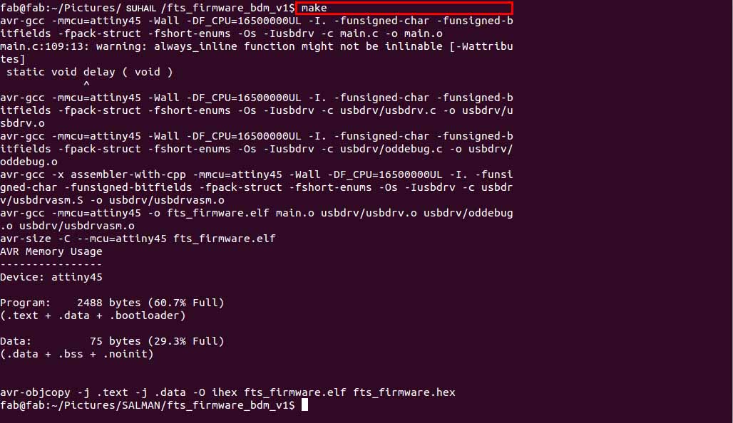
Now we are ready to flash. Open the terminal in the folder path of the firmware located and type
make to make the .hex file. This will generate a .hex file that we need to burn in to the Attiny 45.
Now just type type
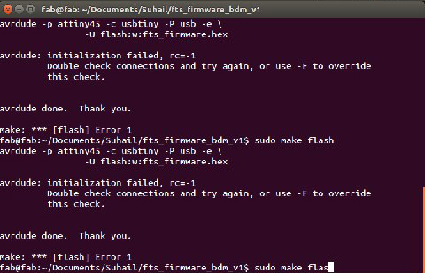
make flash in linux terminal to flash the firmware to the microcontroller.
When i try to flash the firmware, i get uploading errors. I occe again i confirmed every components that i'am soldered is made any bridges or lose conections. But the LED is turning ON. In my view i doesn't made any mistakes. I approached one of my instructor and he helped me. The error is simple as it is, I conected the wire between two ISPs polarity is in wrong. So, i conected them in proper way. This time 'jackpot'. it is uploaded sucessfully.
make fuse in terminal to activate internal fuse.Now we need to either remove the jumber or desable the reset pin. Removing jumper conection is not mandotory, we can disable the reset pin. Its upto you. i choose to desable the reset pin.
If you disbale the reset pin, then the Reset pin will disconected internally. Means you canot program it any more after disabling the reset pin.
If you want to desable the reset pin, then type
make rstdisbl command in terminal. you will get a success message.
After uploading the firmware successfully i need to check the FabISP is working correctly, to do that i need to enter a command in terminal
sudo avrdude -c usbtiny -b9600 -p t45 -v.After entering the command i got the return feedback like this below.
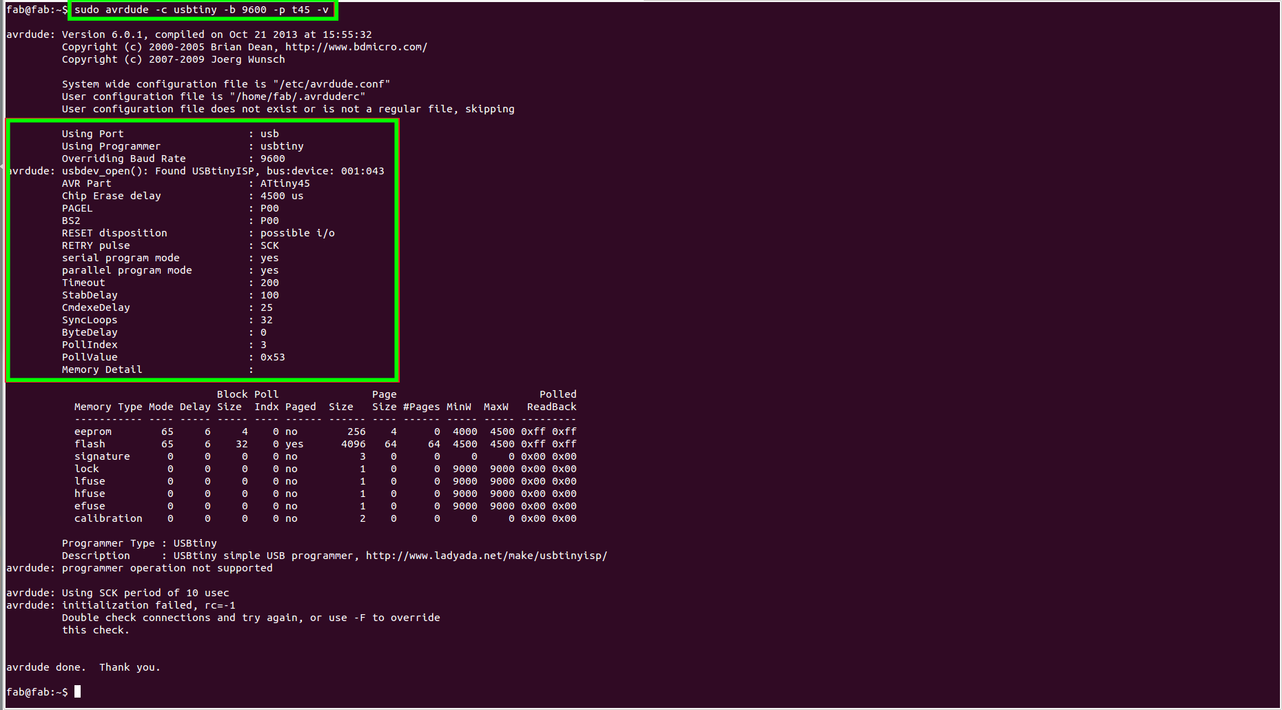
After that we can remove the FabTinyISP. We are done!.
Finished FabTinyISP
Now i can program any AVR microcontroller using my FabTinyISP. Here is the finished FabTinyISP that i made in the fifth week of Fab academy 2018!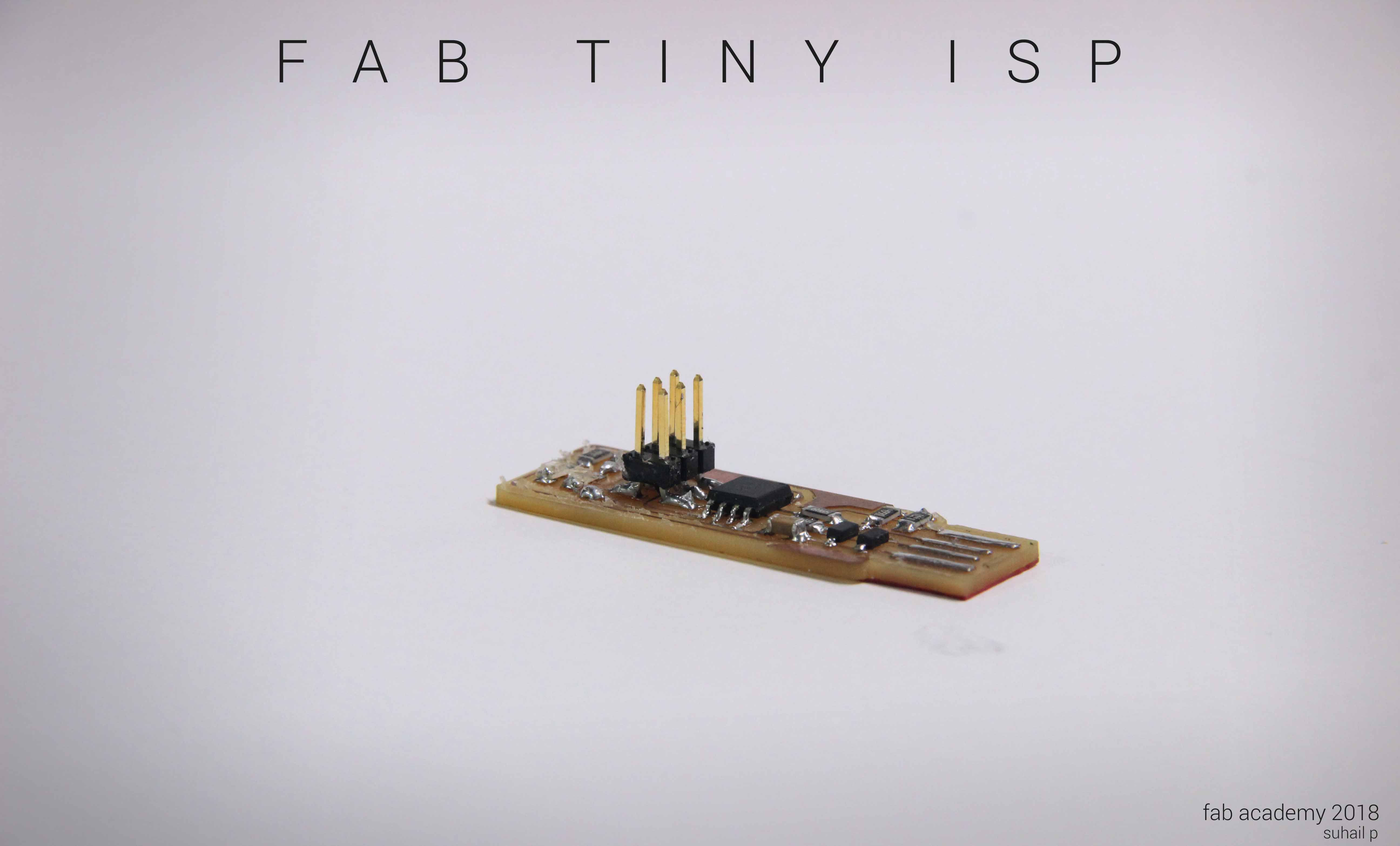
Group Assignment
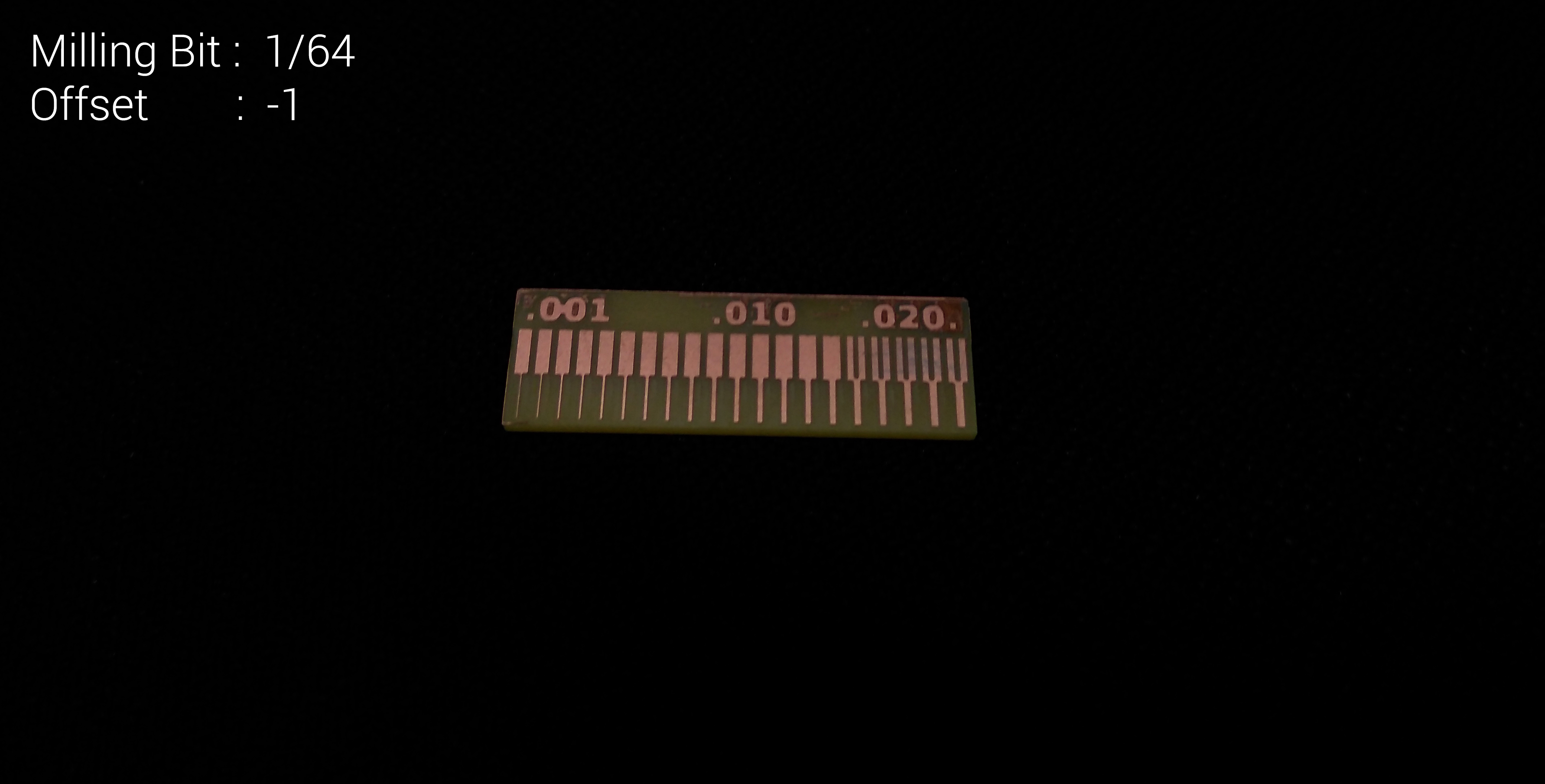
This week group assignment is to characterize the specification of the PCB production process. I'am almost covered everything in the begining of this week. Now all i need to do is find out the reselution differences of different milling bits (1/64 and 1/132). We got a PCB test pad layout. we give a try on it using 1/64 milling bit. We all are so interested awaited to see the results.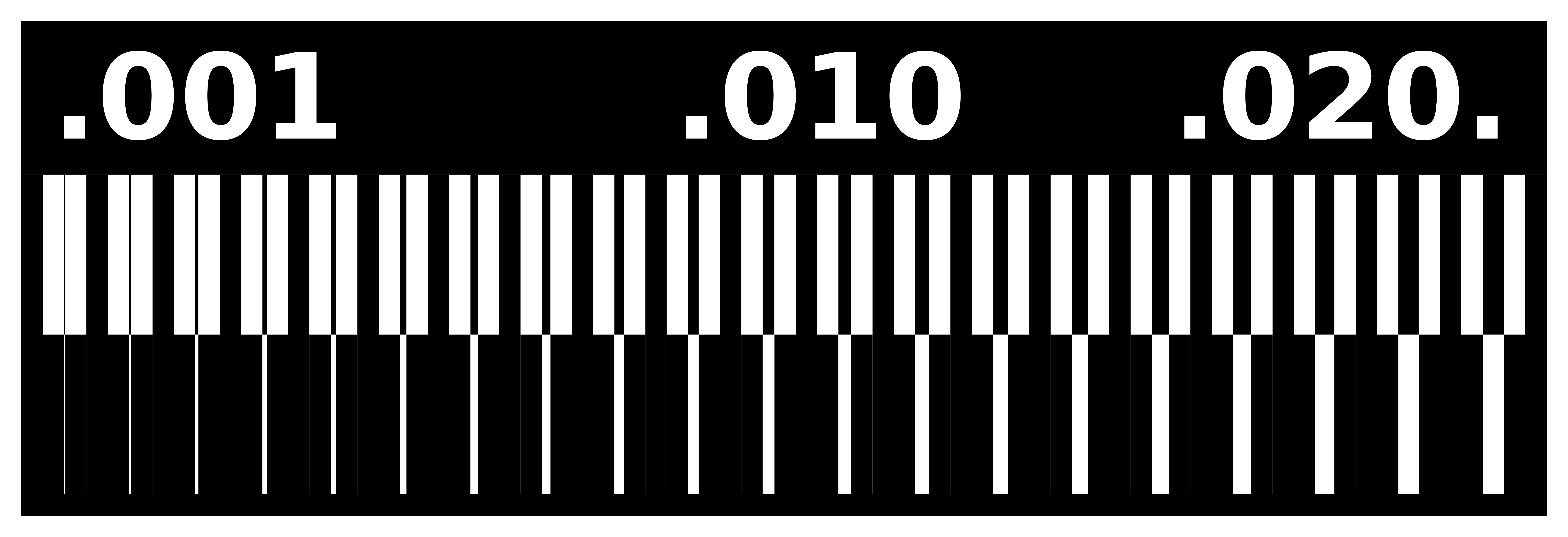
Results of 1/64 milling bit
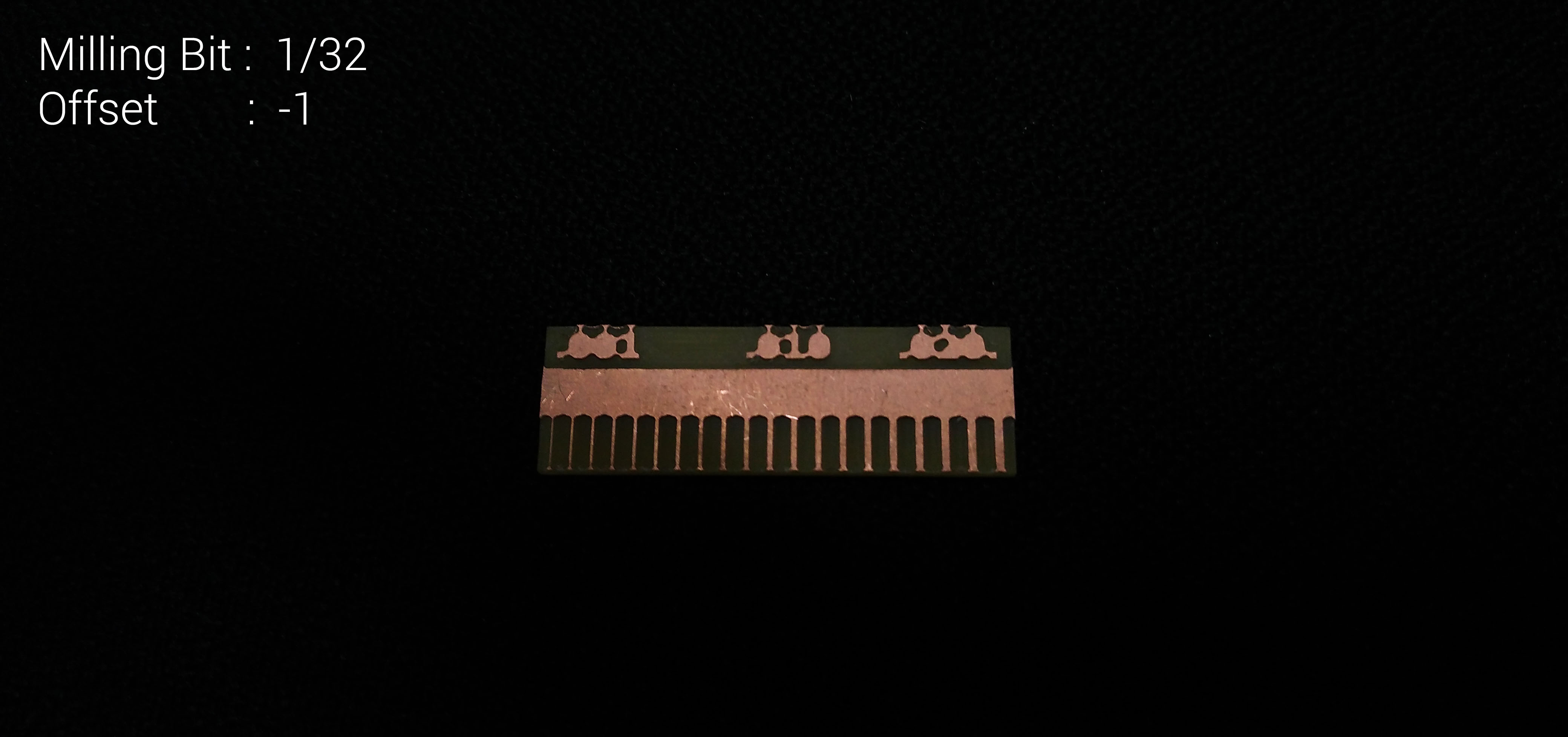
Results of 1/32 milling bit