Week 20

project presentation
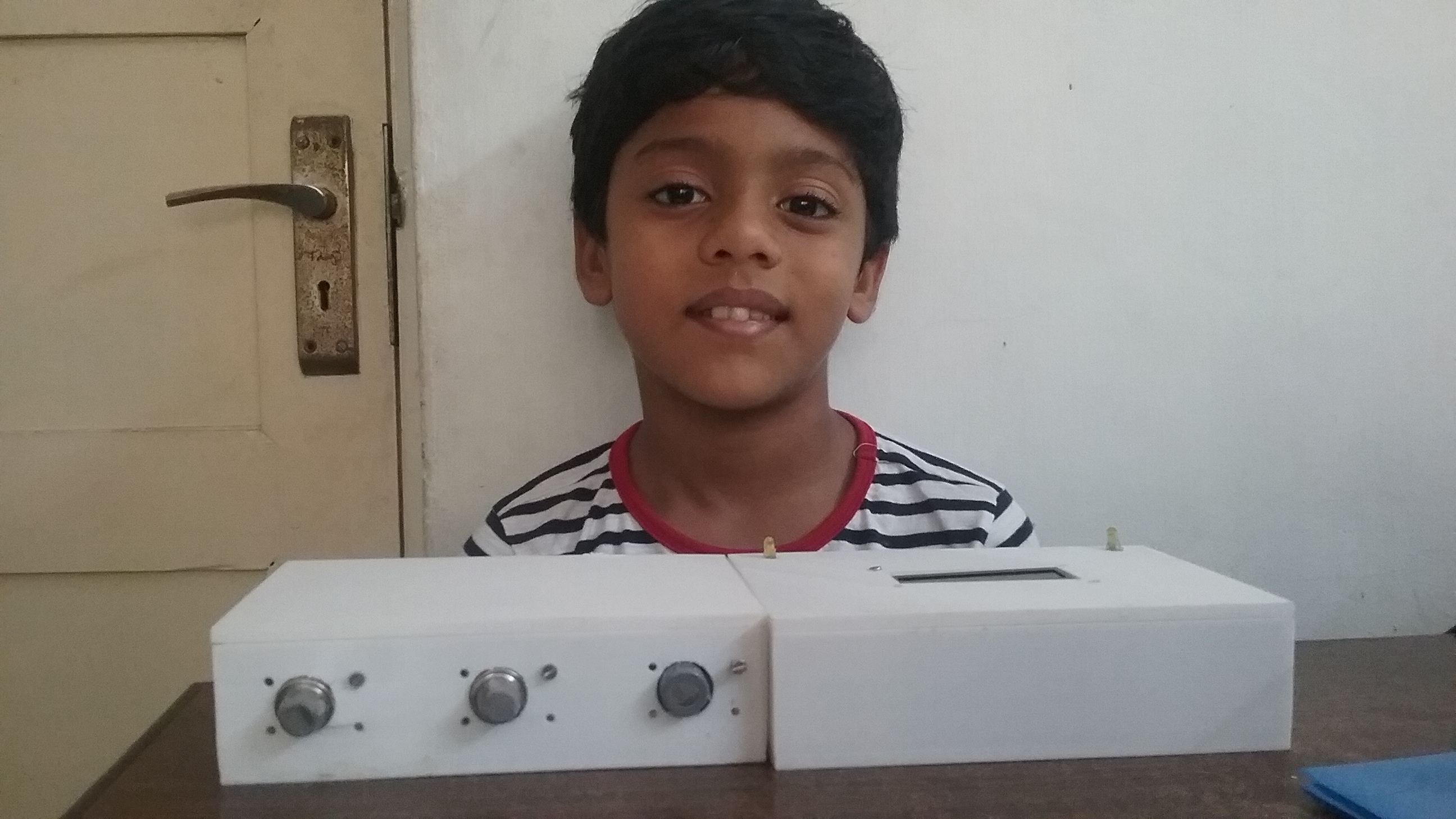
my project is a poisonous gas detection system
In India there is lot of poor people working in well cleaning and sewage cleaning. These poor people does not have any protection from poisonous gases and lot of people die every year in India. Based on my knowledge there is no such device available for the poor cleaning workers. I finally reached an idea of poisonous gas ditecting module for detecting the pollution level.I got this idea after reading an article about such a death in my place. The gas sensor module will detect harmful gases to humans. This module have arduino,gas detecting sensors,and indicators etc. Different gas sensors are used to sense gases. This unit is dropped to the well. This unit is connected to the main unit through serial connector. The main unit receive the message from the sensor unit and then displays appropriate messages on the LCD screen. It also produce warning lights and sounds.
my project inludes
electronics
pcb designing
Electronic circuits in engineering and industry are normally manufactured by using printed circuit boards (PCBs). These boards are made up of special materials that do not conduct electricity such as fiber and glass. The circuits are designed on the boards with copper tracks instead of wires for the conduction of electricity between the electronic components.
The electronic components are fixed in their respective positions by drilling holes on the board, placing the components and then soldering them in appropriate positions so that the copper tracks and components together form a circuit. The printed circuit boards used in all electronic products such as automotives, wireless devices, Robotic applications, etc., offer quick functioning, access, control, monitoring and precise and exact results when compared to other wiring methods based devices The below figure shows how the circuit is arranged on a PCB with copper layer.
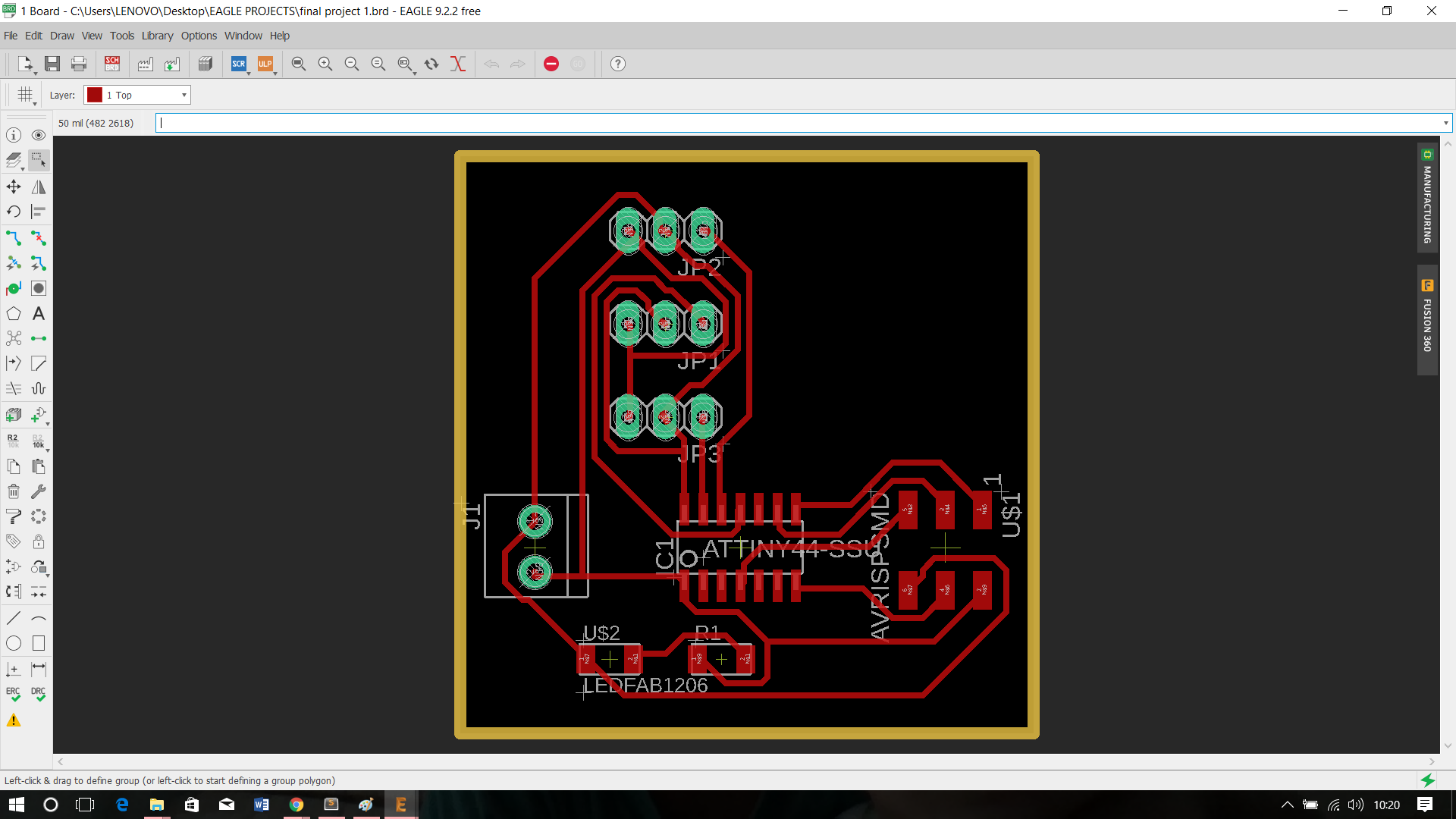
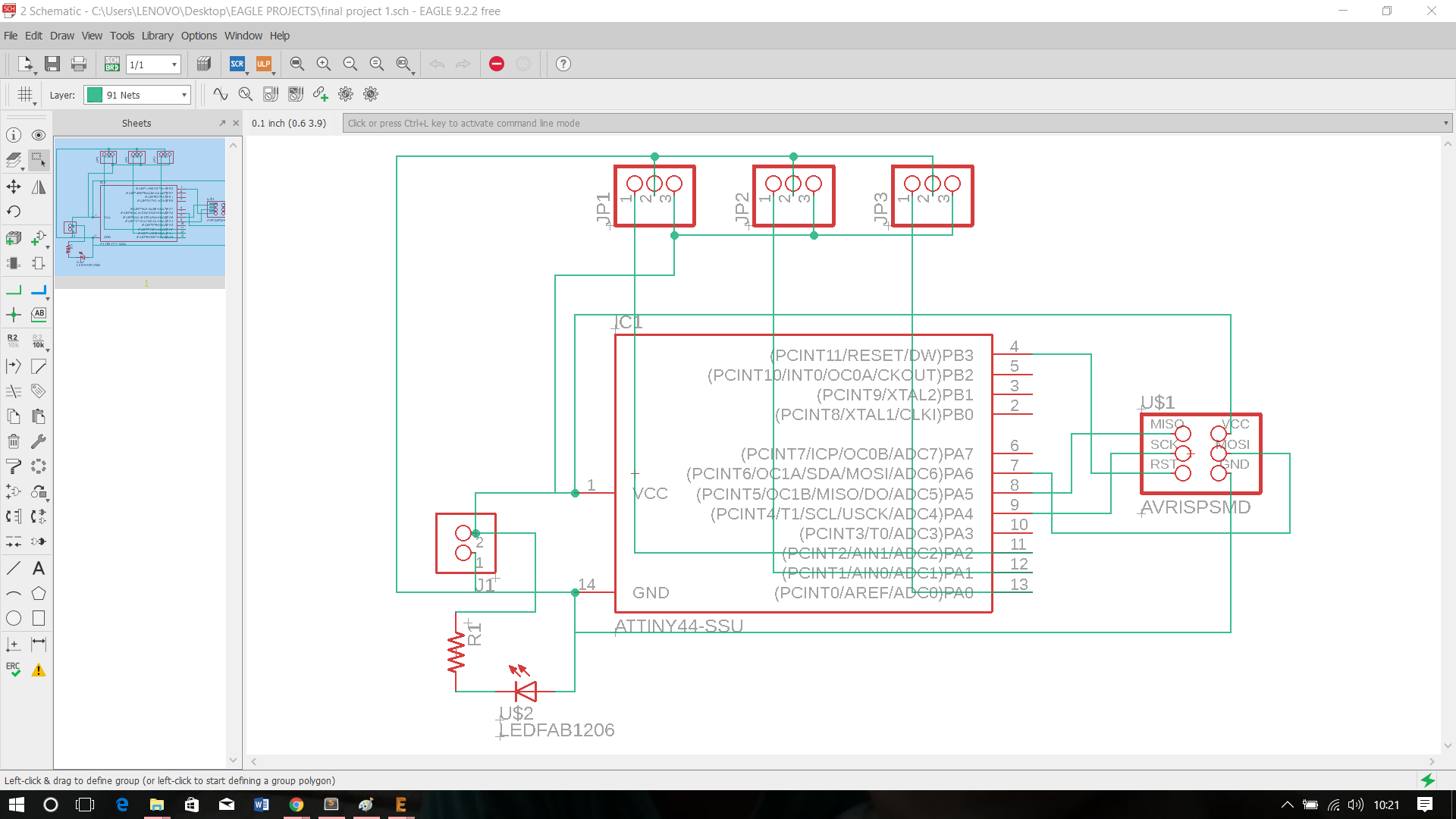
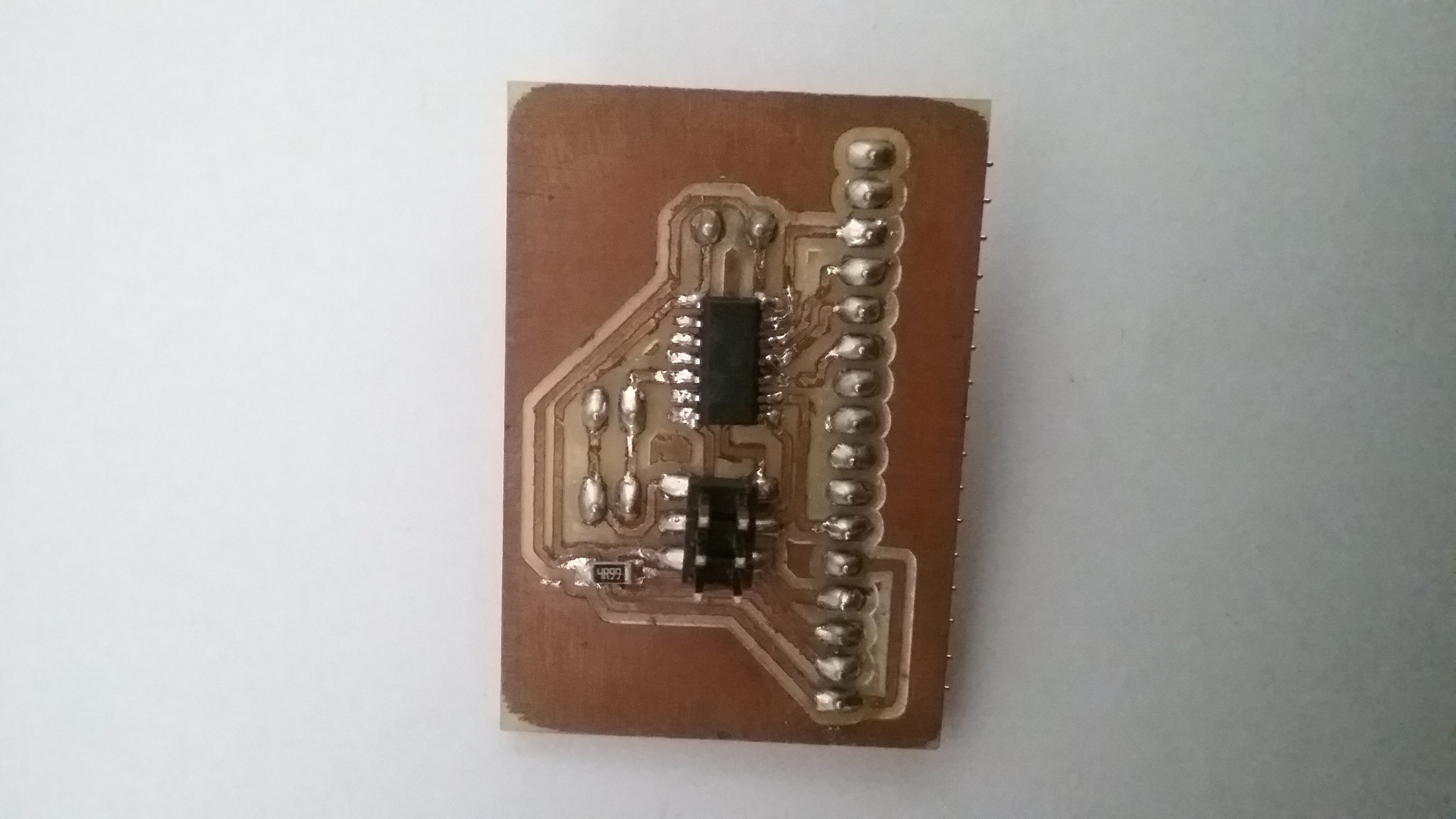
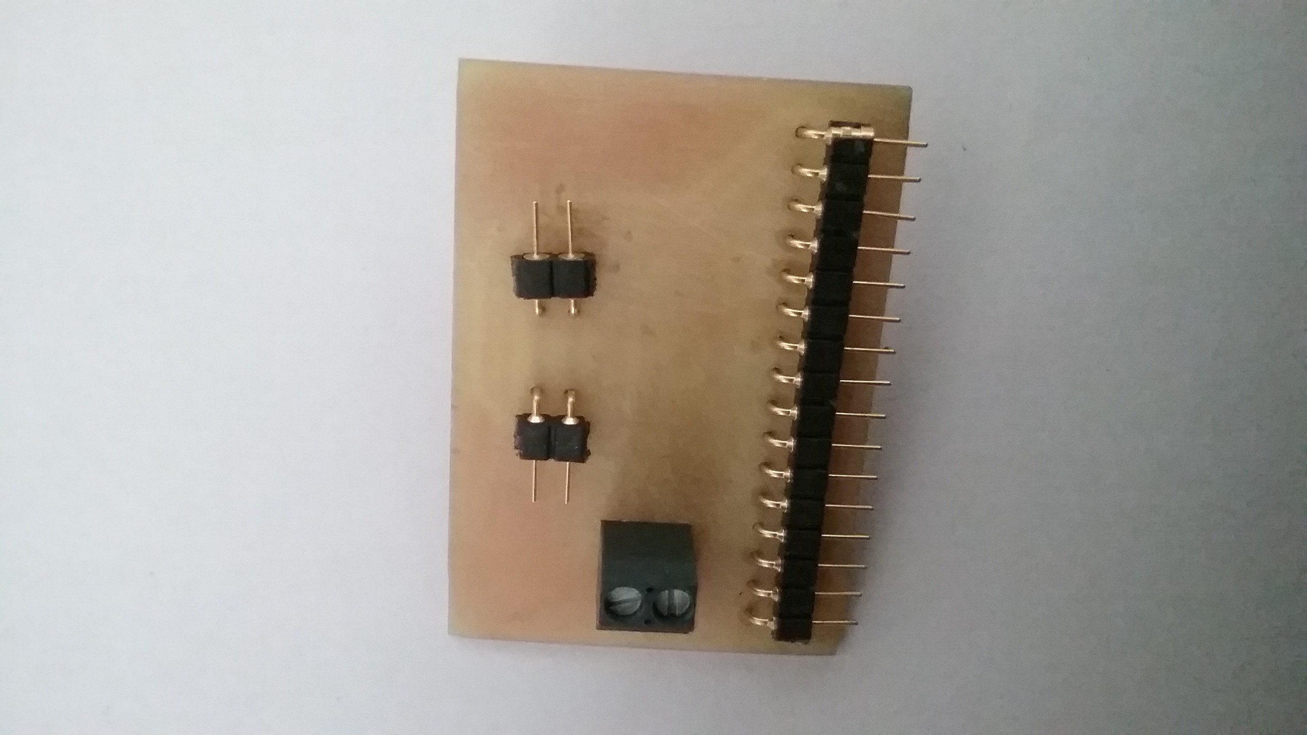
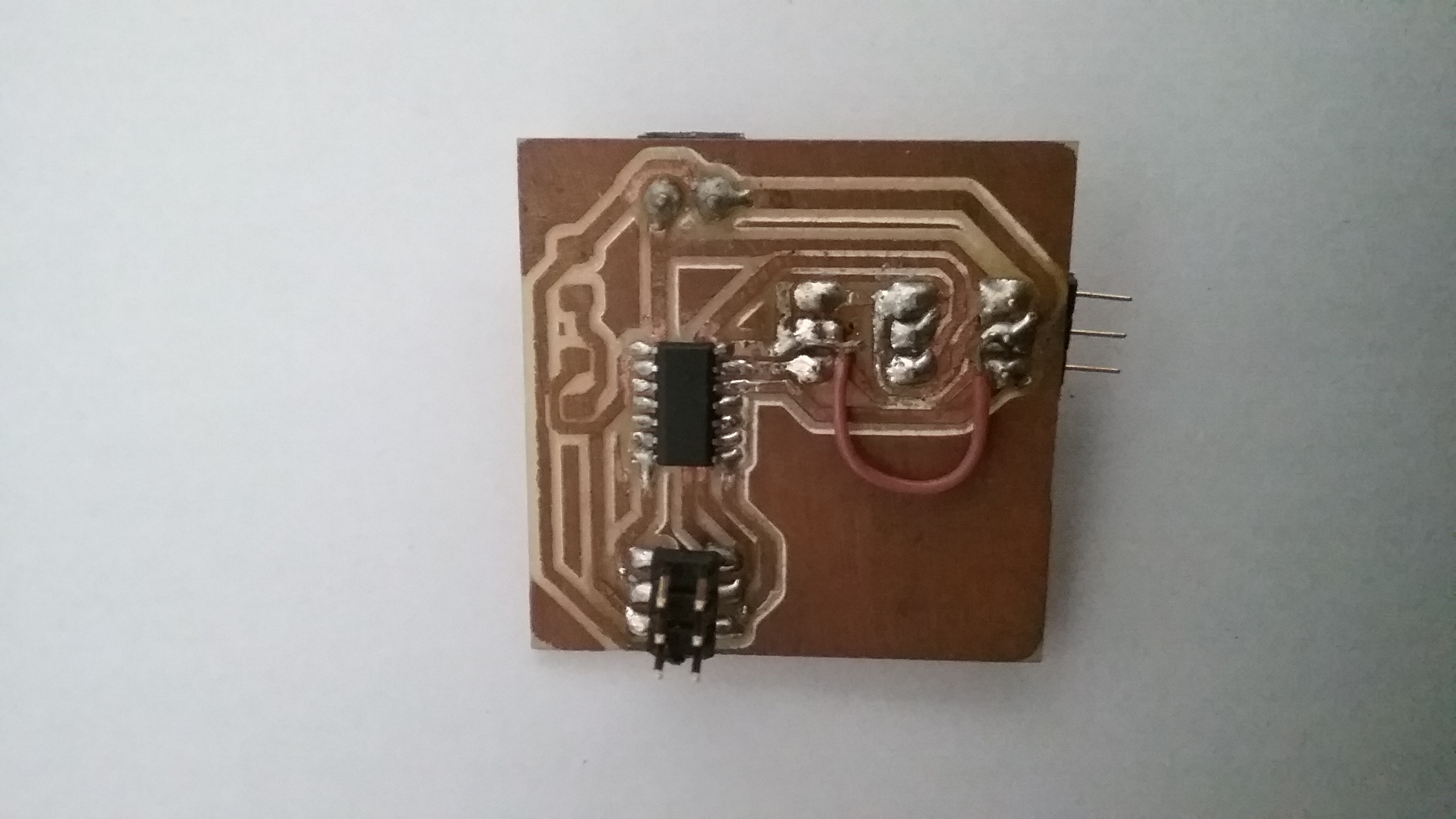
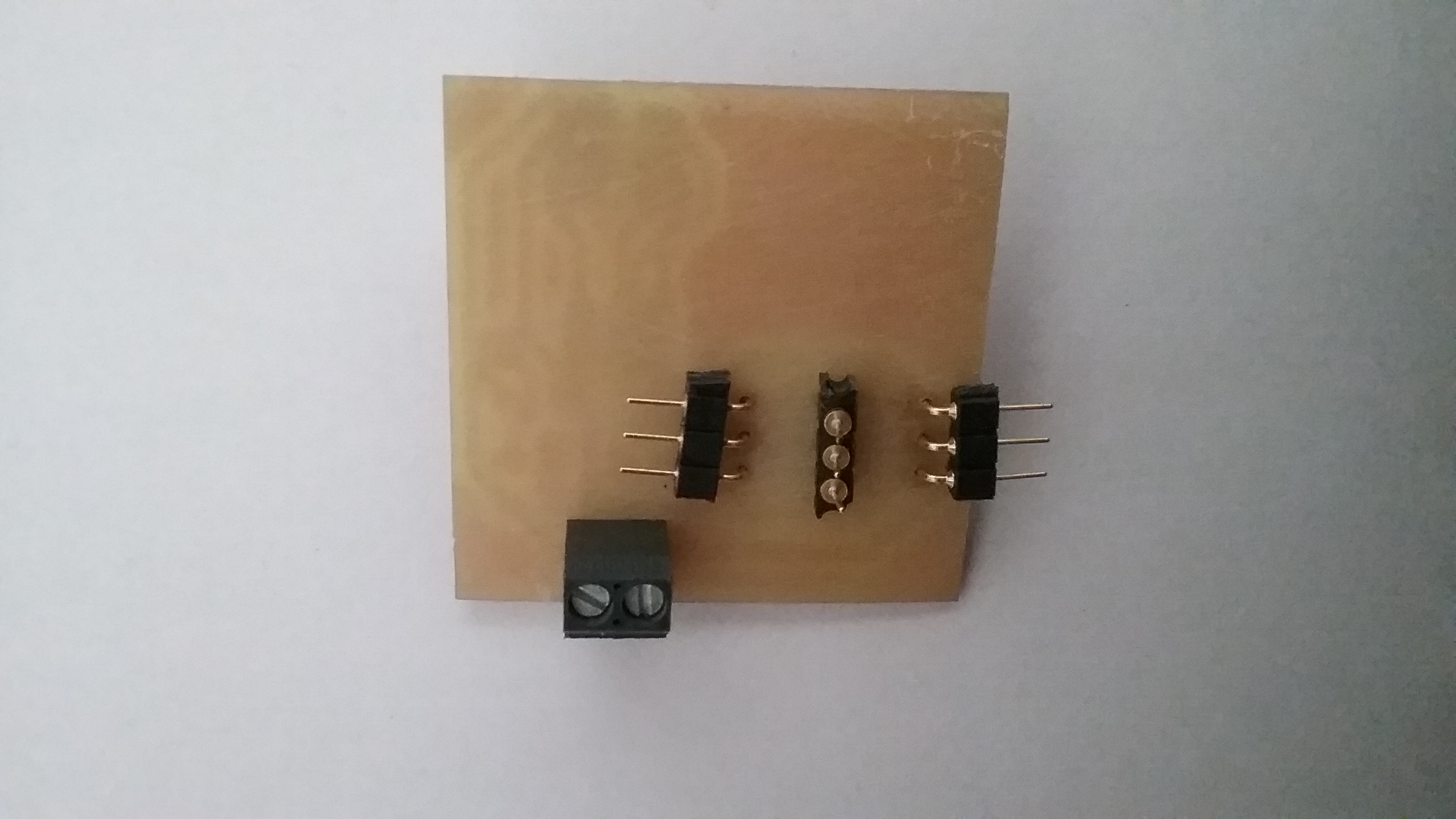
for my project I have to design 2 PCBs
the steps involved in designing are:-
1.Open the Eagle software.
2.Go to file and click new > schematic.
3.Click add button and selest your components.
4.Click wire option and start wiring
5.Then click board button on the top to arrange the board
6.Then press autoroute to make traces
7.Export it
unit 1
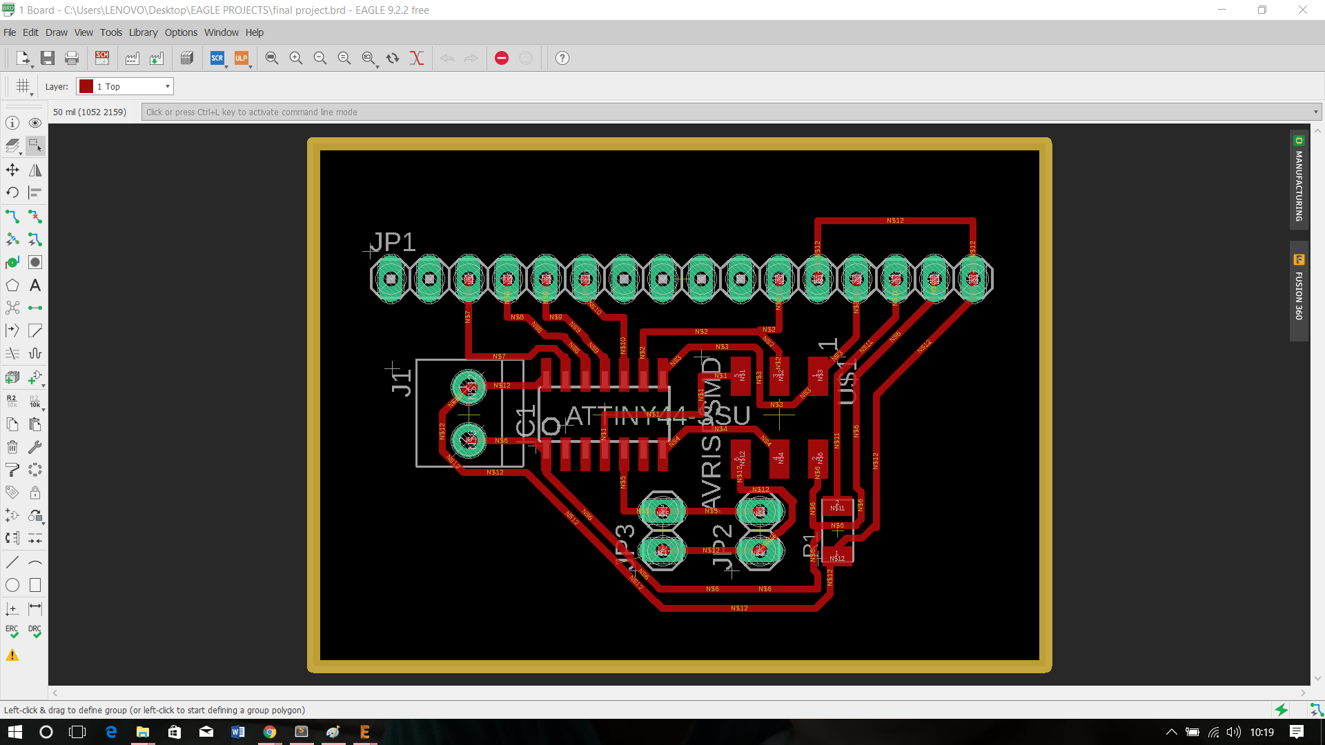
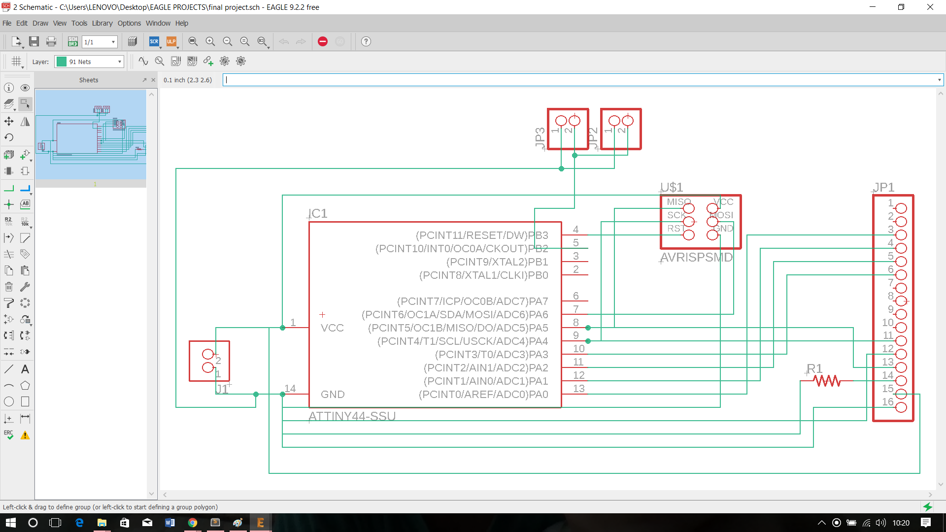
unit 2
milling and soldering
For milling the PCB we used modela in our lab.Modela is a PCB milling machine,which can be controlled by fab modules .The fab modules which accepts the .png extention file and next we move to mill the pcb, for that open Fab Modules and give .png as the input format, select modela as the machine. Then load the traces .png file and then make path. Leave the settings as such. I learned how to mill the PCB using miller and learned fab module also.I learned how to solder the components in the PCB in the 5 week of this course. It is fun soldering.
the components used are:-
1.attiny 44(2)
2.2x3 pin header(2)
3.terminal(2)
4.3x1 pin header(3)
5.2x1 pin header(2)
6.16x1 pin header(1)
input and output
I used input and output for communicating with LED,LCD DISPLAY(gives alerting message),SENSORS.
The sensors are
MQ135
MQ5
MQ7
.
It is for detecting gases like:-
Carbon momoxide,carbon dioxide,ammonia,methane etc.
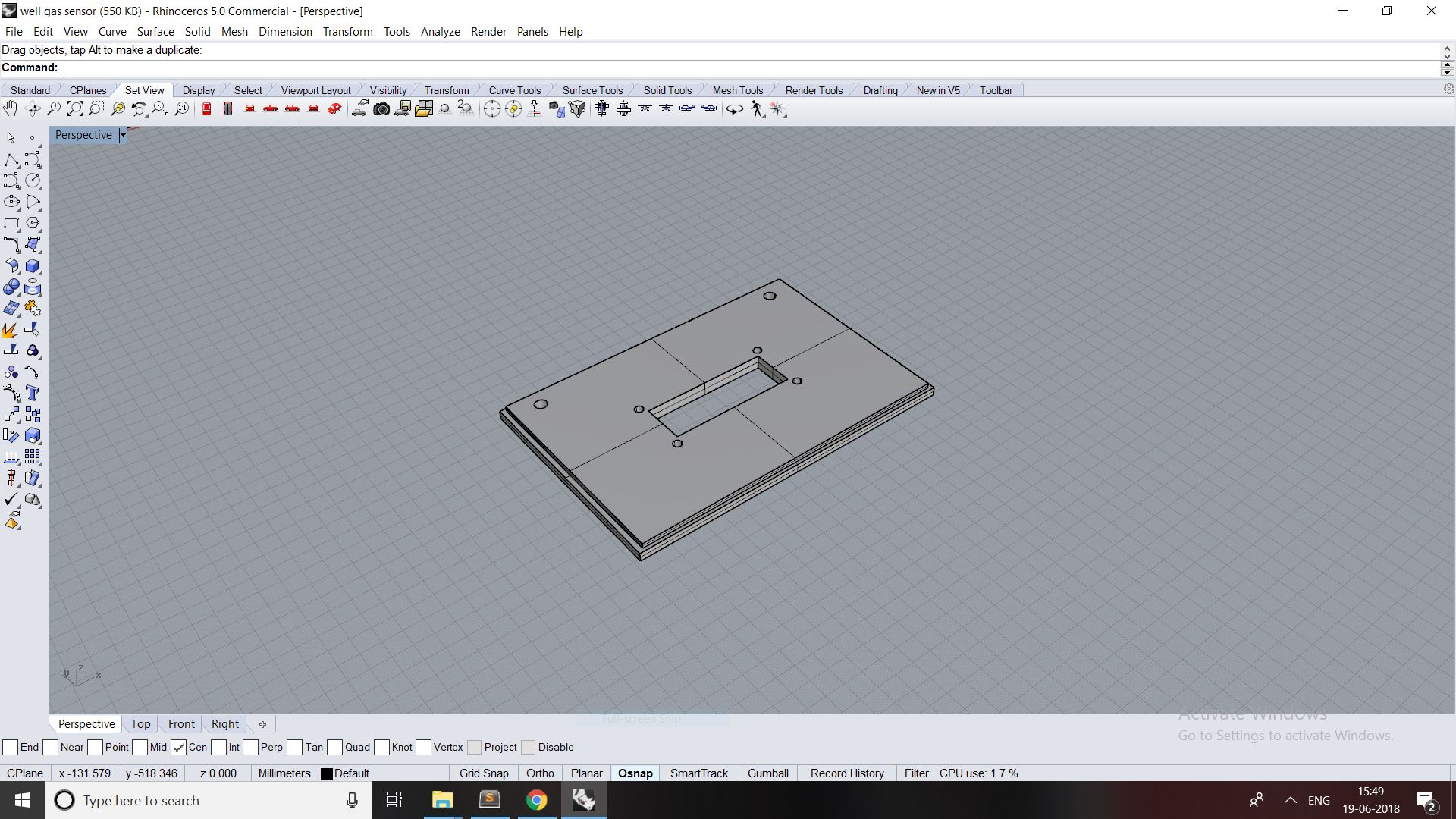
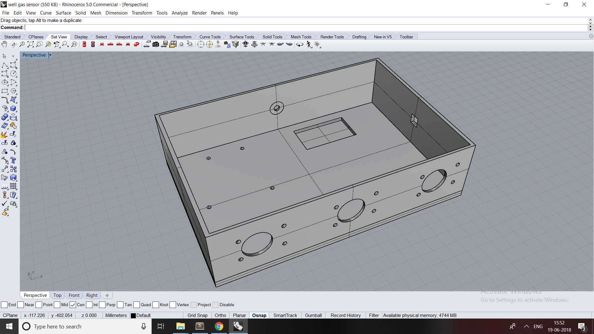
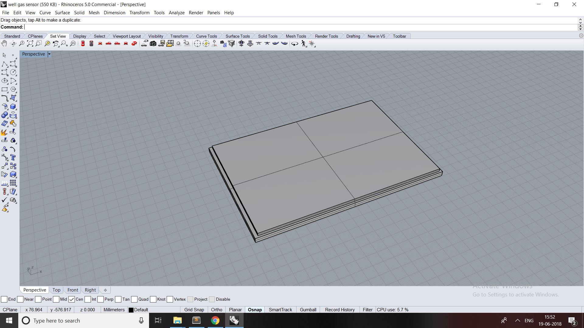
3d printing and 3d designing
3D printing is any of various processes in which material is joined or solidified under computer control to create a three-dimensional object,[1] with material being added together (such as liquid molecules or powder grains are fused together). 3D printing is used in both rapid prototyping and additive manufacturing (AM).The term "3D printing" originally referred to a process that deposits a binder material onto a powder bed with inkjet printer heads layer by layer. More recently, the term is being used in popular vernacular to encompass a wider variety of additive manufacturing techniques.3D printing is an innovative technology that lets you create a physical object from a digital model. It started in the 80’s under the name ‘rapid prototyping’ because this was the purpose of the technology: to prototype faster and cheaper. A lot’s changed since then, and today 3D printers offer amazing results and let you create anything you can imagine.
designs
Interfasing with RX and TX
It means that comunication between two or more things.
Here we are comunicating with RX and TX.
The message is passed from one unit to another wiht the help of serial wire.The sensor detects the poisonous gas and send the data to the micro controller.Then it will send it to another unit where the micro controller receives and show it in the display.