

Electronics Design
This week is about "Electronic Design", I like such weekly tasks in which there is any electronic part. On 28th of the February, Sir Prof. Neil gave us online lecture about this week's related tasks. After His lecture I became able to clear my few queries regarding circuit production. In this week our task was to design echo hello world board.
Tasks of the week
Group Assignment
Individual Assignment.
Group Task
Digital Multimeter
"A multimeter is for electronic engineer as stethoscope is for doctor". It is most convenient and helpful equipment when we test or measure electronic components. We decided to check component in echo-hello world circuit using multimeter to confirm the values of components and to check either they are in working condition or not.
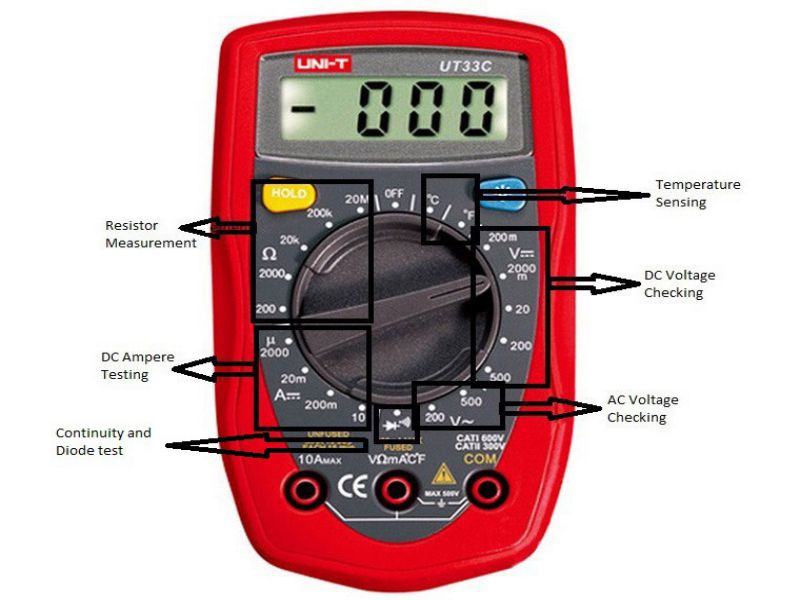
Continuity check and Diode testing
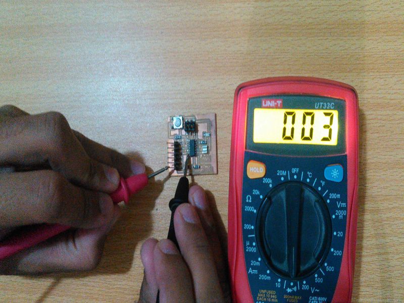
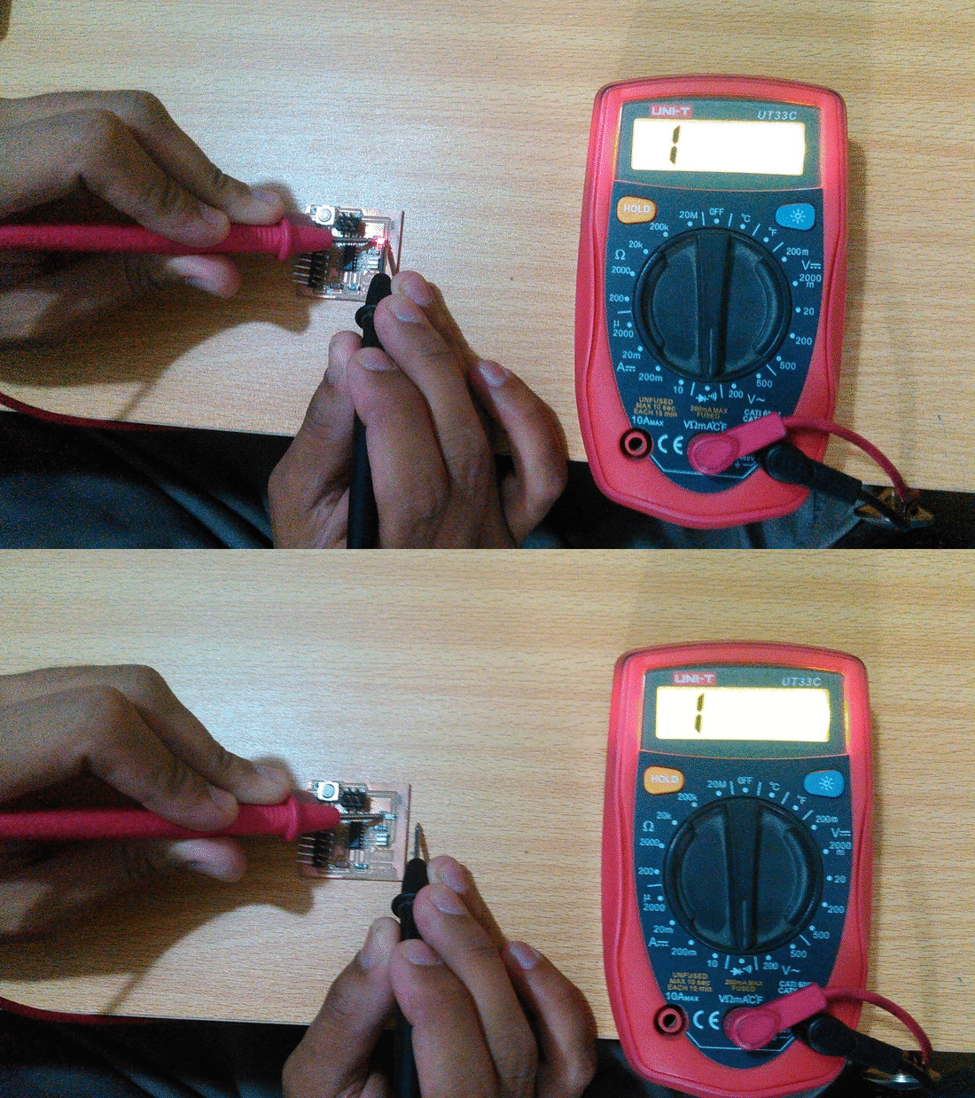
To test the continuity and diode first turn the dial of multimeter on continuity testing function which is mentioned in above picture. Continuity test is done by checking circuit tracks with probes, if beep occurs it means that tracks are connected if there is no sound of beep or shown "1" on screen it means that tracks are not connected.
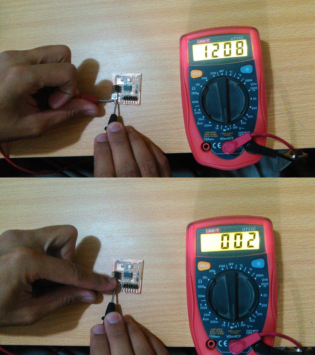
To check the LED we placed the black probe on cathode side (which is marked green in our LED) and red probe on anode side, if LED glows it means that it is in working condition.
Measuring Resistance
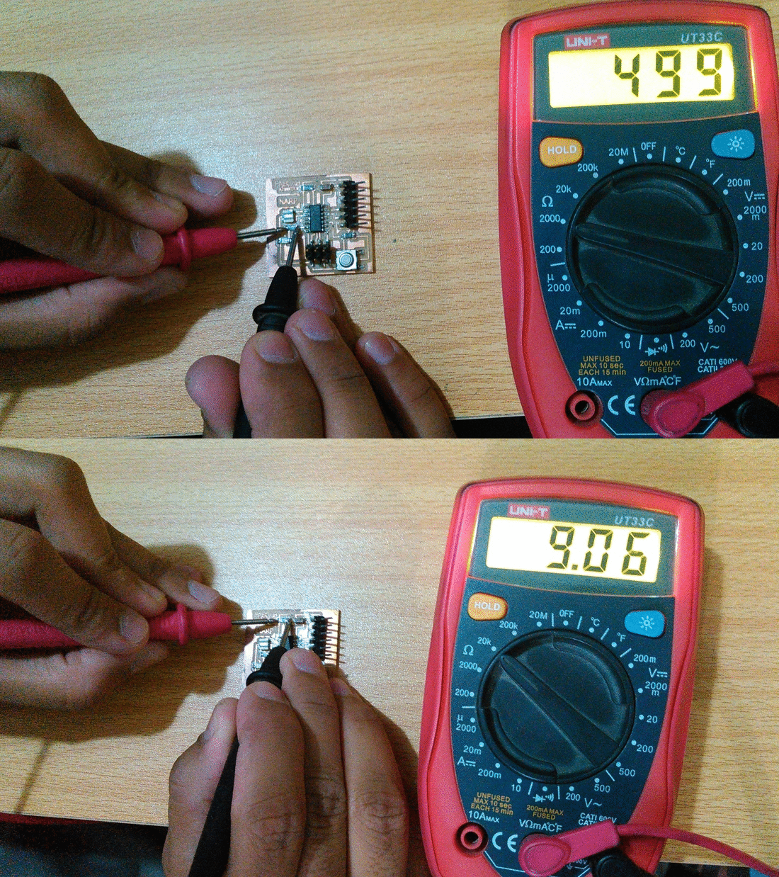
In a echo-hello world circuit we have 3 resistors, 2 are 10k ohm and 1 is 499 ohm resistor with 1 % tolerance. To check their values we moved the dial to "20k" in resistor measuring portion and measured them.
Voltage Measurements
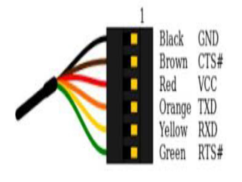
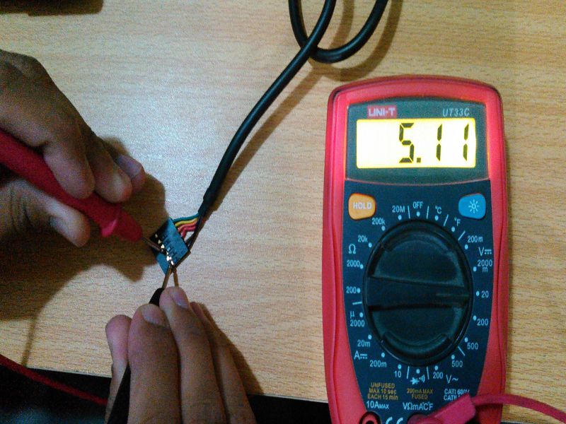
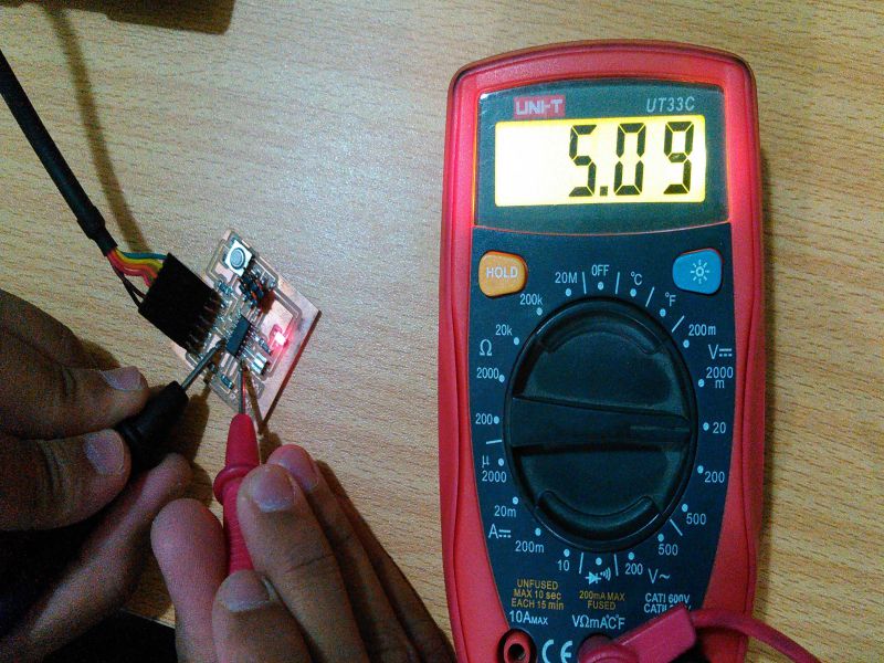
A circuit is powered via FTDI cable which has 6 pins in which black one is GND and red is VCC. We checked the potential difference by placing black probe on GND pin and red probe on VCC pin to check the voltage. Then we check voltage in circuit by powered it with FTDI Cable.
Individual Tasks
I redraw the given board of prof.Neil in eagle. As I am bit familiar with eagle software for designing the PCB boards, so it was not challenging for me to handle this week task. Here is the Neil's board: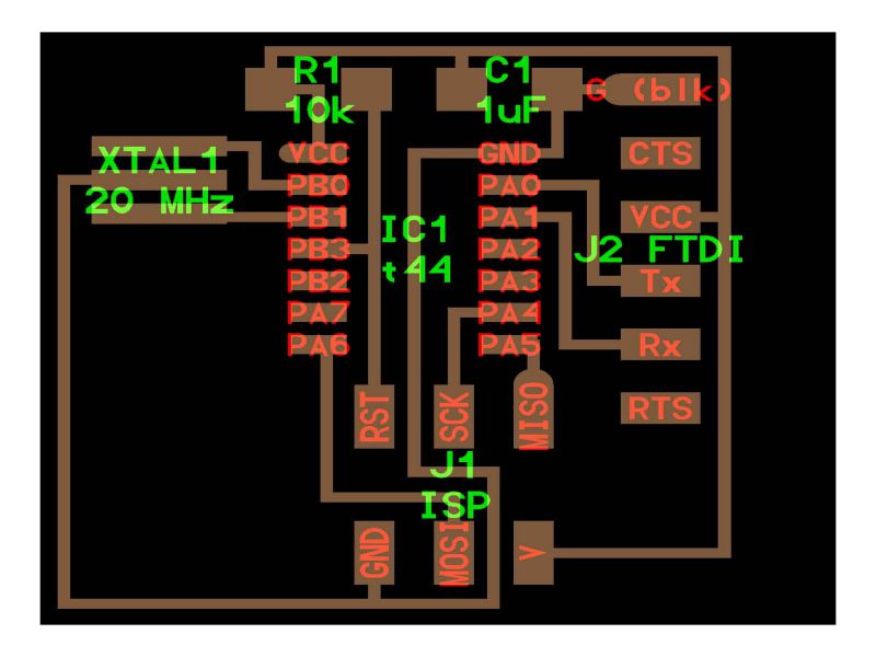
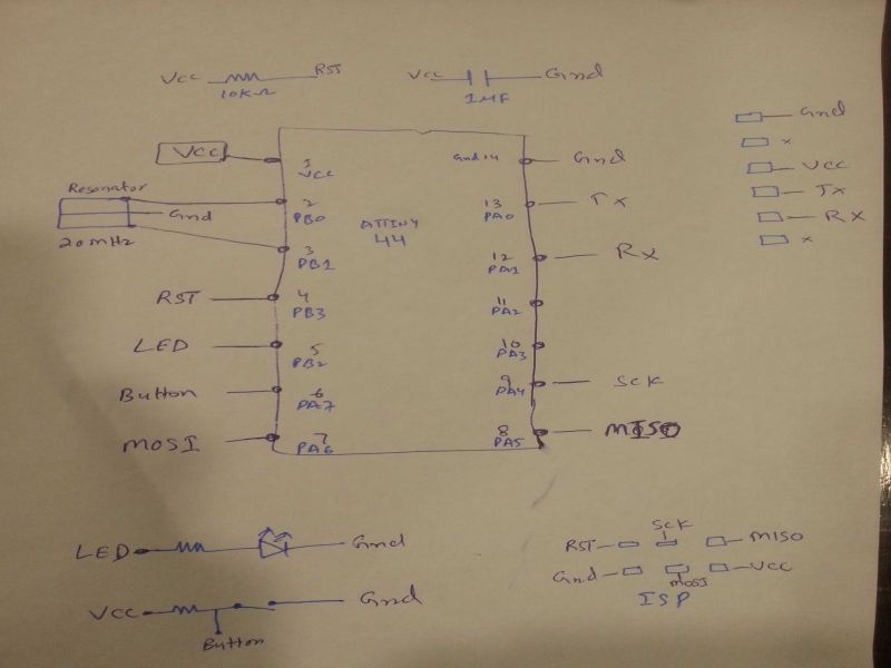
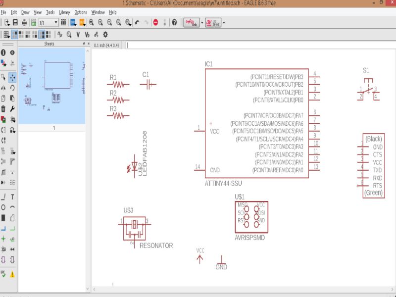
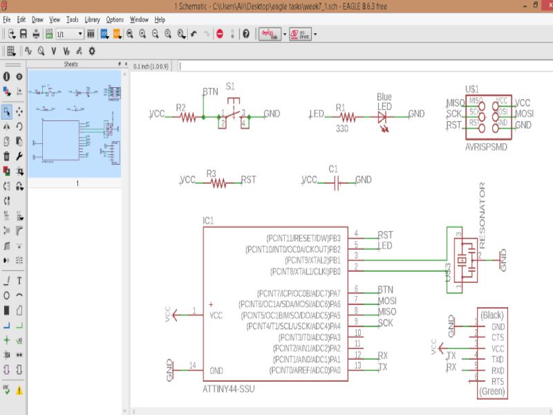
I sketch the schematic of the board on a page then I followed the sketch on "schematic" part of eagle according to the specified pins.
Eagle software for PCB designing
Here, I choose Eagle CAD software for designing the PCB boards, I choose it because I worked on this software in my Final Year of my bachelors degree. In my opinion it's very easy to work with it.
And, it provides well known features like printed circuit board layout, auto router, and computer aided manufacturing. I am handy with using Eagle cad software for designing of my PCBs.
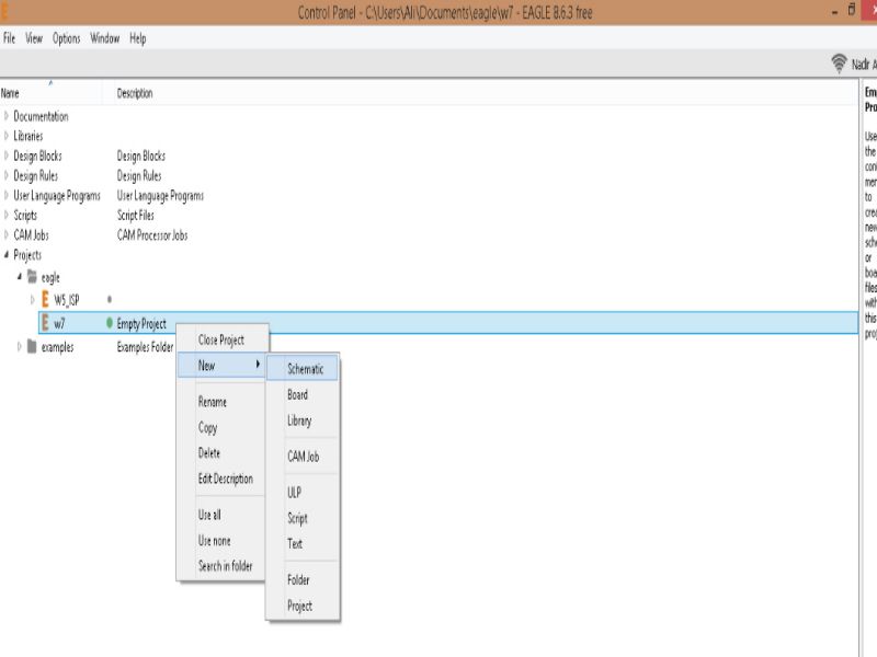
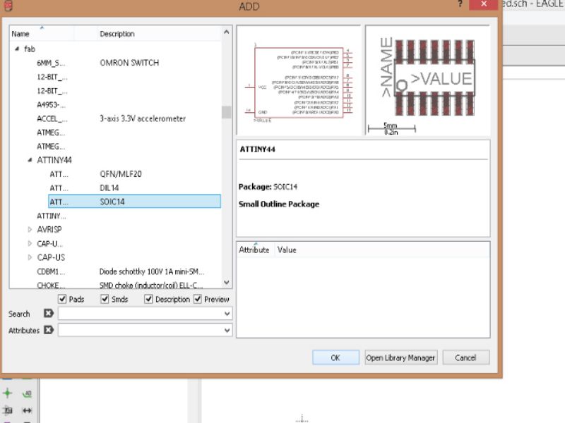
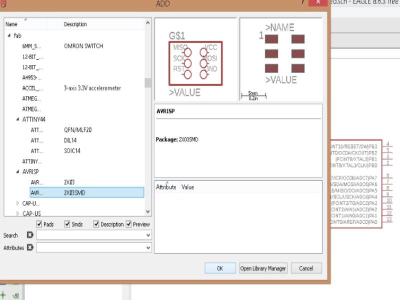
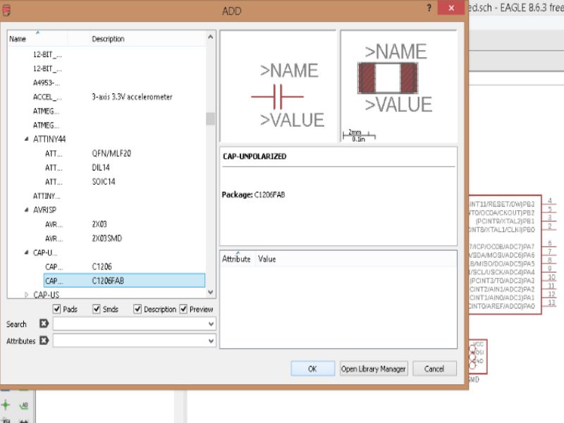
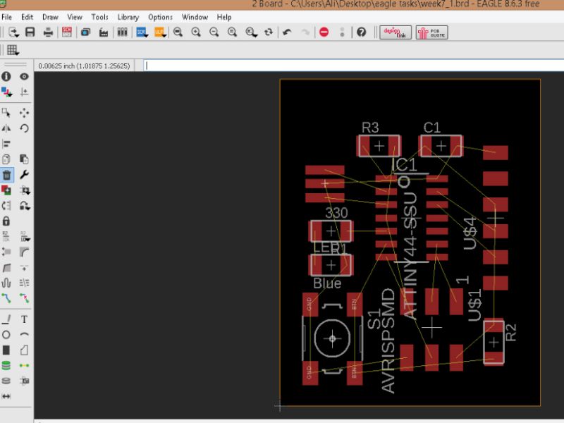
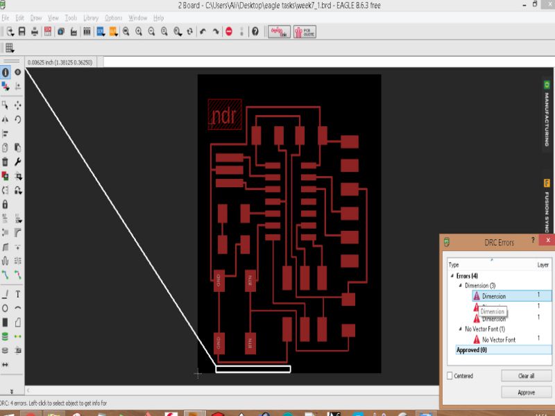
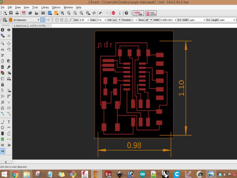
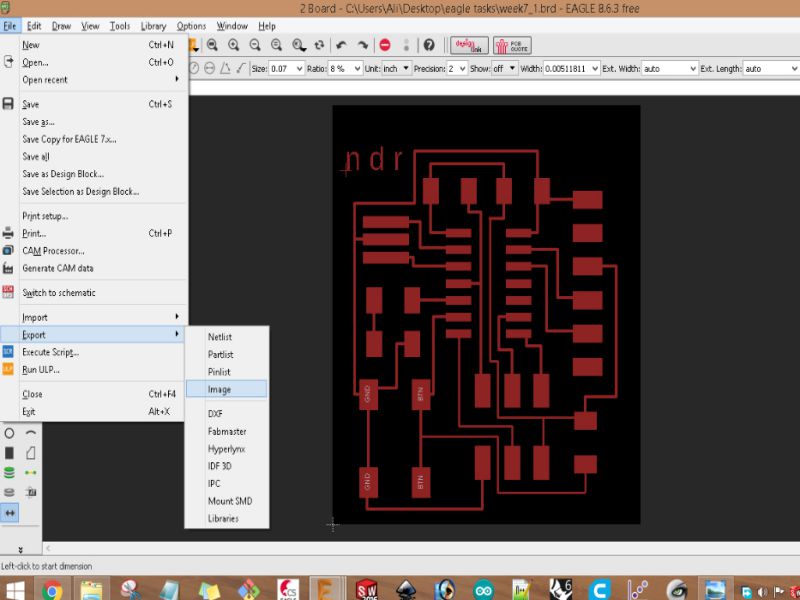
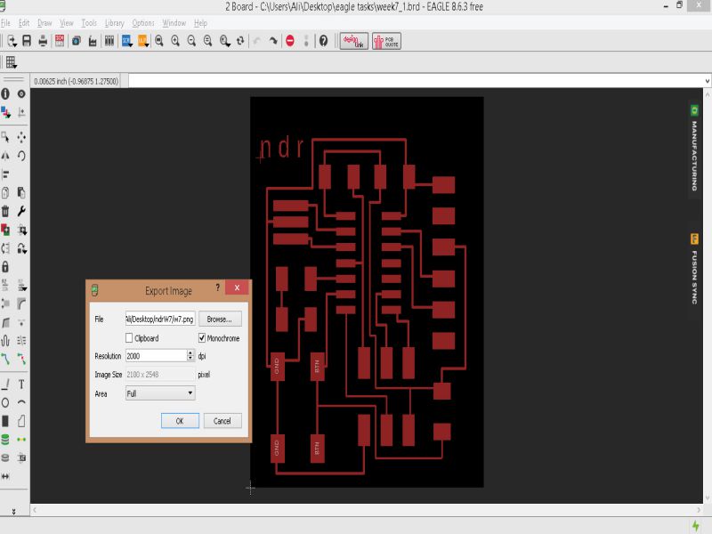
Step by step process of designing the board on eagle are shown below:
Design Rules:
Layers: The layers tab defines which signal layers the board actually uses, how thick the copper and isolation layers are.
Clearance: The clearance tab in eagle defines the various minimum clearance values between objects in signal layer. The actual minimum clearance between objects that belong to different signals will also be influenced by the net classes the two signals belongs too.
Size: The Sizes tab defines the minimum width of any objects in signal layers and the minimum drill diameter.
The width size of objects/components which I used in this board are mostly of 2mm (~0.08in).
The minimum width of the route which i drew are 0.006 inches. It will be good if we use the route line width as 0.012 to 0.016 inches.
Distances:The Distance tab defines the minimum distance between objects in signal layers and the board dimensions, as well as that between any two drill holes. The minimum distance in traces which I used in this board are about 0.64 mm.
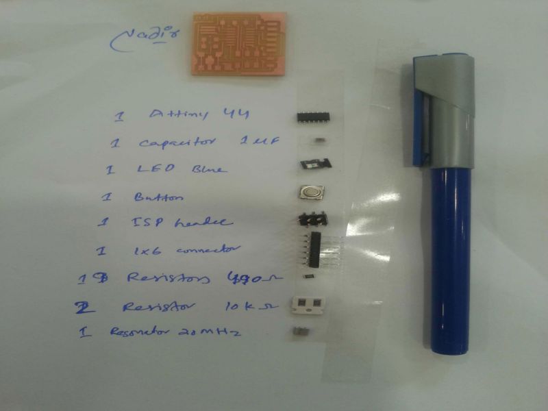
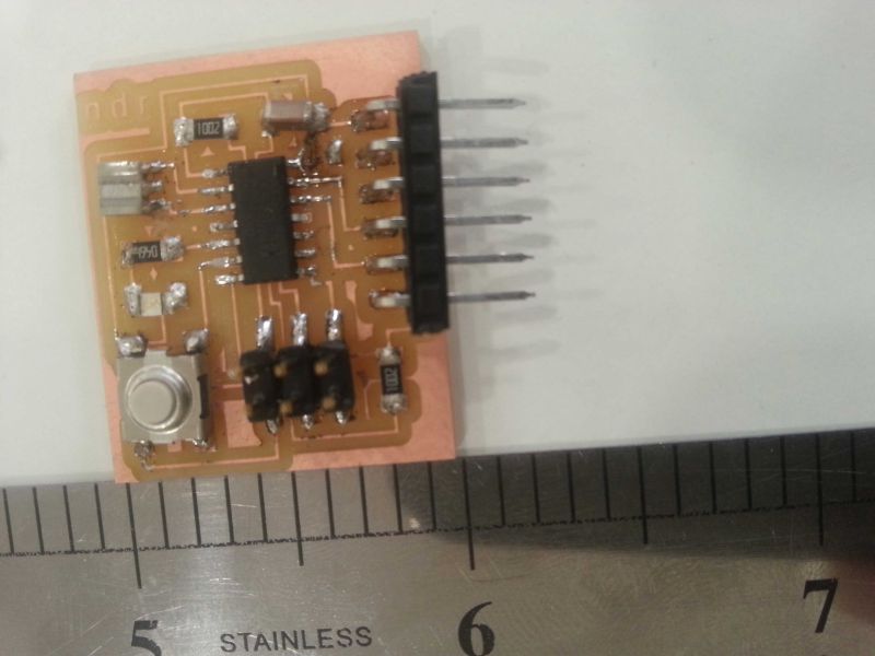
Debugging the circuit
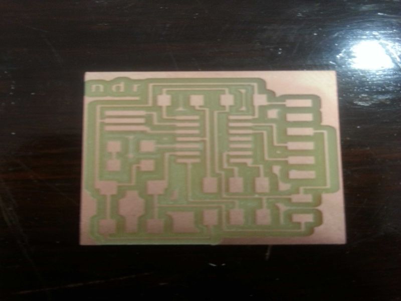
After soldering the board, now the next step is to check the connectivity and proper flow of the source into the board. This process is called debugging the board that is checking the connectivity of the paths and checking proper flow of source in the circuit on each component, And also mitigate the main problems which disable the board to circuit. To find out the error, we have to use digital multimeter which helps us to point out the problems, if any. So, for that I used digital multimeter, I checked connectivity of ground, VCC and other pins of microcontroller. When this step completed successfully, I jumped to the next step that is up the circuit. If this process is out of error then there is a huge chance of up the board successfully.
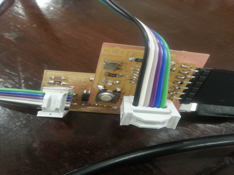
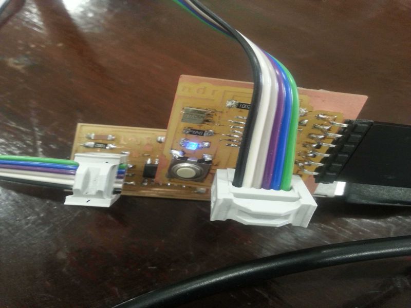
Now it is the time to burn boot load the circuit.
Here I burn bootloader successfully through AVR ISP circuit board. Blinking images of the circuit are shown below:
Learning Outcomes
- Datasheet must be refered before using any component/MCU in designing circuit. I used attiny44 microcontroller in this week task, that is 14 pin IC.
- It requires special attention to sold SMD components.
- Mature placement of the components can reduce the size of the board and also helps to route easily.
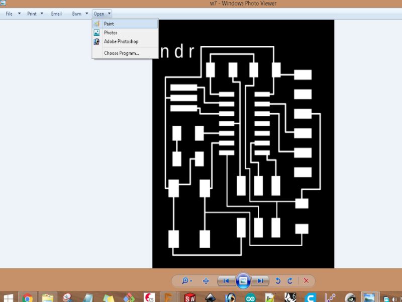
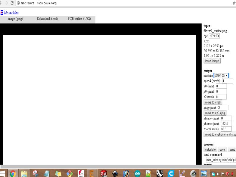
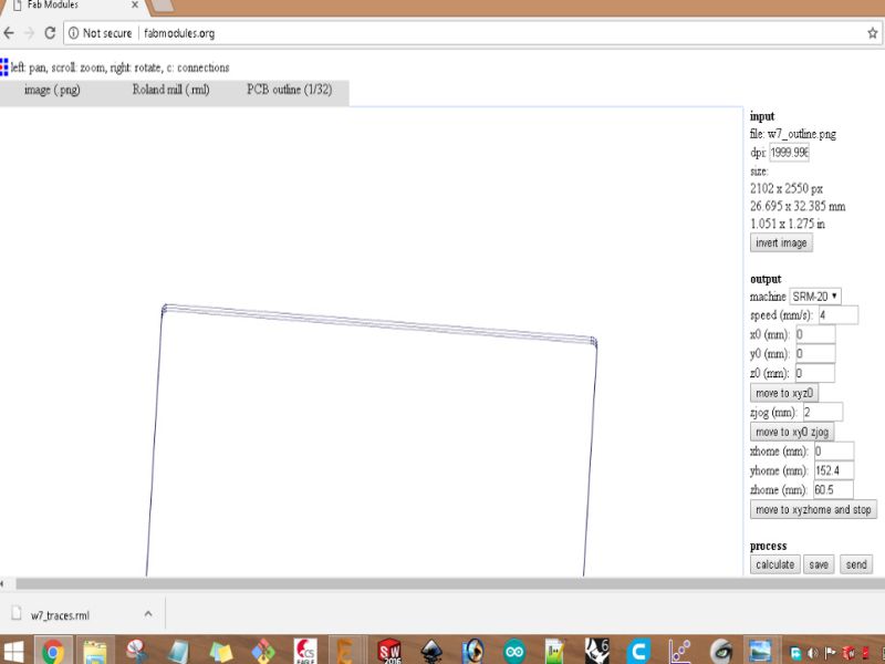
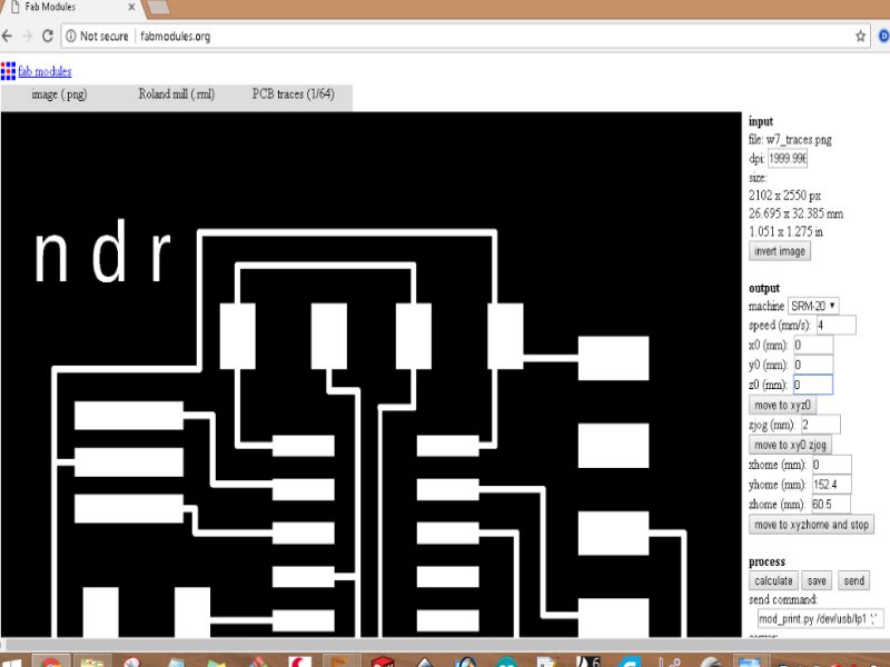
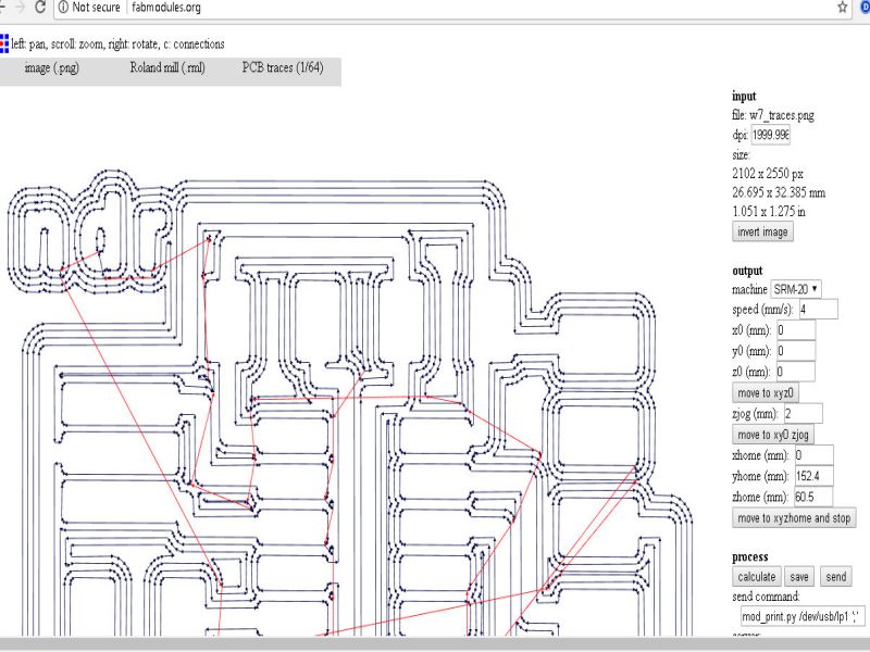
- For generating .rml files in 'Fab module', the resolution of exported image must be greater than 1200 dpi, I select 2000 dpi in this circuit.
- Selecting of PCB desgning software also plays a vital role to reduce complexity. Here I used 'Eagle' as I also used it in my previous weeks of electronics circuit designing.

This work is licensed under a Creative Commons Attribution-NonCommercial 4.0 International License.
