add (at least) a button and LED (with current-limiting resistor)
check the design rules, make it, and test it
extra credit: measure its operation
extra extra credit: simulate its operation
Research & Acknoledgemnts
Hence it is possible to use other microcontroller than the Atttiny, I thought I would make a board for my final project but it turned out that my design would require componets yet to be ordered, so I focussed my design solely on the Hello World board.
Originally I wanted to use CircuitWorks (Altium incorporated in Solidworks environment) but due to local hardware constraints (No powerful enough windows machine, which I borrowed from my university) I decided to use Eagle .
Although I tried KiCad, I found Eagle to be more intuitive.
Eagle provides a free version which is provided for Windows and Mac.
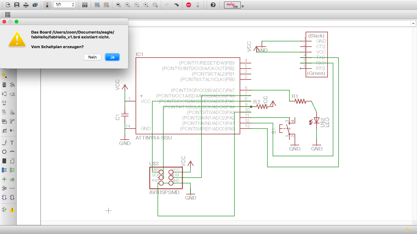
One does start a Project by “File” > “New” > “Project”. On the left side there will be a File-Manager where you can type in the name of the new Project. With right clicking the mouse on the project a menu pops up. “New” > “Schematic” you can create an empty schematic file.
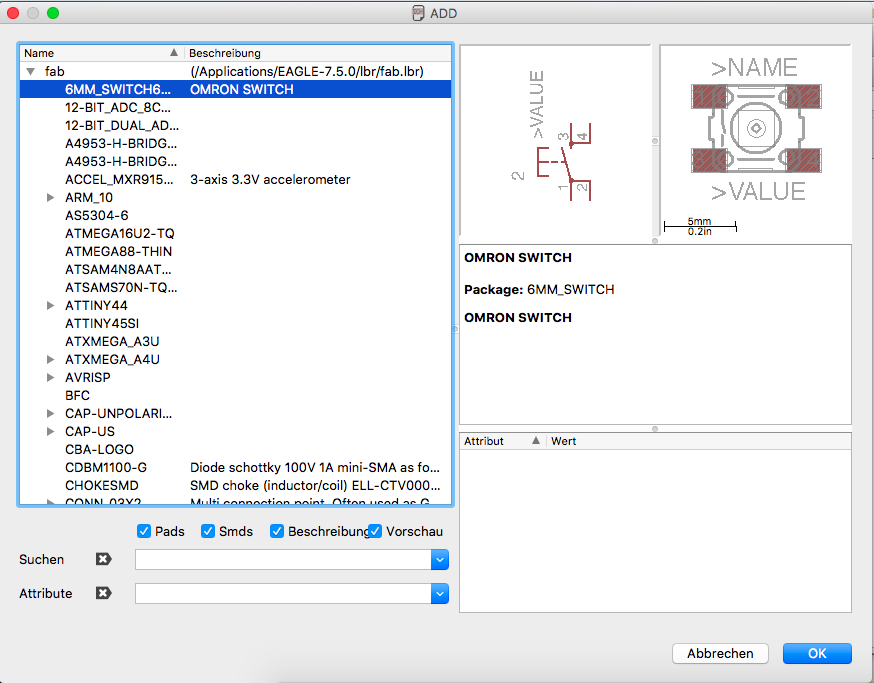
After installing there will be a “Library” directory which you have to find out. To which you copy the fab-library Link. The library contains layout of footprints and annotation for each component.
Then when ever you want to use a standard component from FabLabs, you can go to “Edit” > “Add” and there will be a dialogue where you can type in fab and you can find all the components you need. Double click and and you can insert the component into a scematic.
Design
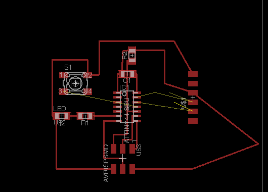
To create the schematic is the easy part. You keep adding the required component. Connect them with “Draw” > “Wire” option. At this step it was crutial to move the parts a little bit to see whether they are indeed connected, because I had many failed attempts where I thought it were connected, when it was not.
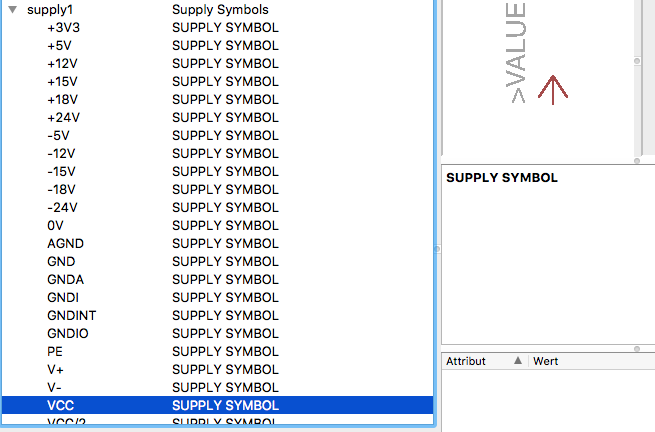
While designing, using VCC and GND symbols are recommended for the sake of better overview but it is not crutial, since when creating the layout all the “redundant” connections can be ignored, which I found out later on.
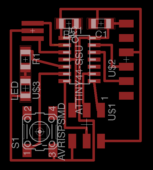
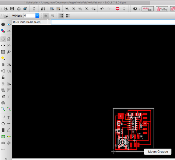
To create Board, select from menu “File” > “Change to board” and it will give you a nest of components on a dark background. You can mark them via Group-Selection from the left tool bar and right click somewhere in the void where “Move” will apper and you can move all the parts at once in the area.
It is recommended to roughly place the whole nest on the lower left corner since the outline of the board (the resizable white rectangle) has its origin there.
Since not all PCB mills can do double sided milling (reorienting the other side is somethimes troublesome) you should keep in mind not to use vias or the back-side in this context. If you are fully aware of that and your mill supports it well, like on the Othermill, then feel free to make use of them.
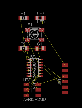
Now to the “fun” part. You can rotate a part with the combination “Ctrl” + “left click” on the center of the part (there is a cross on that). You try keep rotating the parts until you minimized the amount of intersecting yellow wires. Of course you can move a part to minimize the number as well with the “Move” tool from the left tool bar.
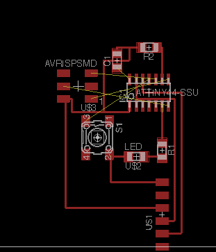
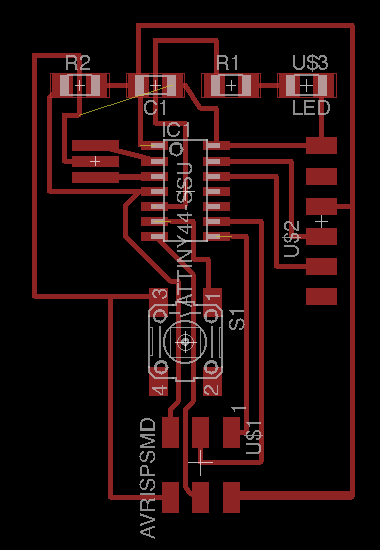
This minimizing step is crutial for the actual routing with the “Route” tool. It is similar to the schematic designing, but this time the “wires” or “route” is final. What you see is what you get.
At first, I was eager to compleately to “find out” the route design on my own, which I archieved, but it looked quite ugly. After some iteration I just looked at the design of neil and added my twist to it. Specificly, he had a route where three routes were routed through the ATttiny pins which in my case even though pressing shift for turing off the rough rastering of the routes looked impossible to mill. So I hade to route it around the whole circuit but it worked out quite fine.
Final:
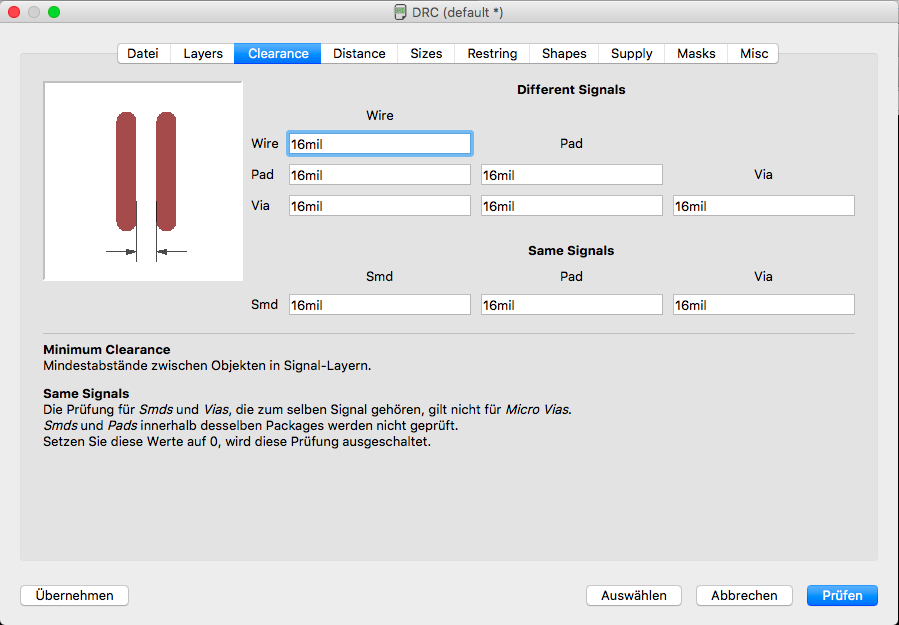
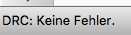
To confirm that the final routing is compliant with the final width of the traces it is useful to do “Tools” > “Verify Layout (DRC)”. And if it runs without problem, which was in my case.
To move it as group:
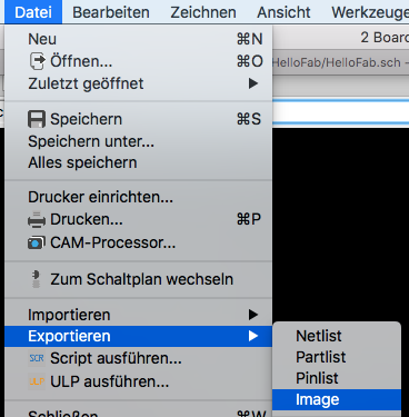
There are two ways of exporting. If you are using mods, you want an image, but if you are using other CAM (in my case Bantam Tools) then you can just save it and import the brd file into it.
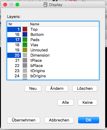
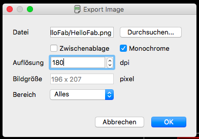
To prepare your design for exporting image, we need to seperate between the outlines of the board and the traces. This can be archieved by (de)selecting “View” > “Layout preferences” and for the outline obviously “outline” and for the traces you want to activate “Top” and “Pads”. When you have selected either of the configuration, you can go to “File” > “Export” > “Image”. Here is examplar configuration.
Fabrication
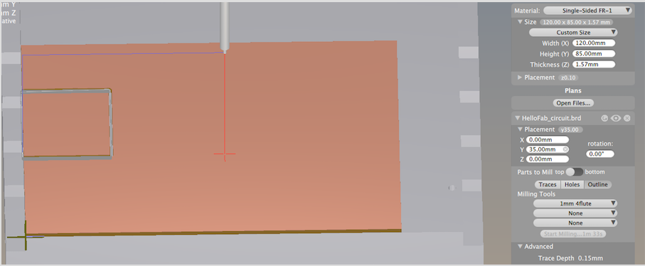
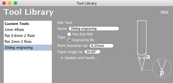
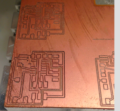
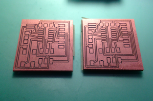
Hence I wanted to try how I could only use the Bantam Tools to make the PCB I sticked to the simplest configuration.
Furthermore I wanted to tryout using a engraving bit (which is more robust and cheaper than very fine mills which can break easily). After configurating the tool in the software, as usual I measured the thickness of the board and started milling, but the tip of the engraving bit was so fine, it did not reach the board. Manually testing the deapth 0.1mm offset was necessary to have viable results.
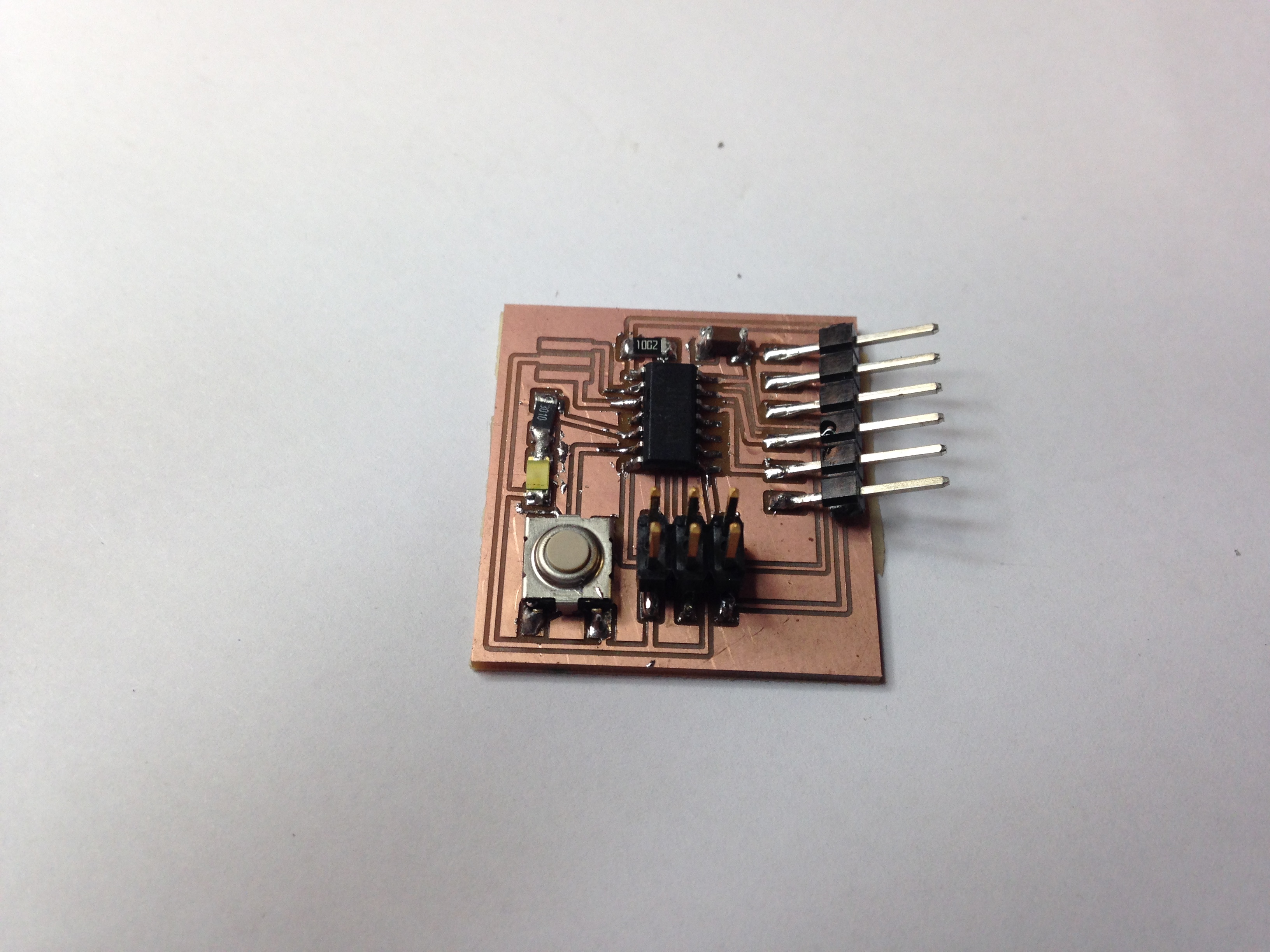
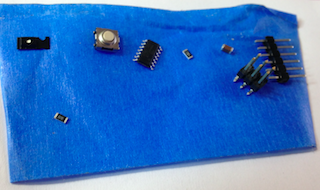
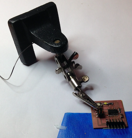
Like the electronics production week I gathered the necessary components before assembling. I found it useful to hold the pcb with a “third hand”.