Week 11 - Input Devices
This week, I decided to use the assignment to prototype part of my final project. FOr that, I’ll need to read a bank of switches (mechanical or photo-interrupts) to identify a particular media card. The board needs to be able to read, say, 10 switches simultaneously and convert that into a number between 0 and 1023, sending it back to a computer over a serial connection. For this project, I decided to use a microcontroller with plenty of input pins, the ATMega32U4.
Group Assignment
We used a multimeter and an oscilloscope to measure analogue and digital inputs: http://fab.academany.org/2018/labs/fablabbrighton/students/derek-covill/group-input.html
Planning the board
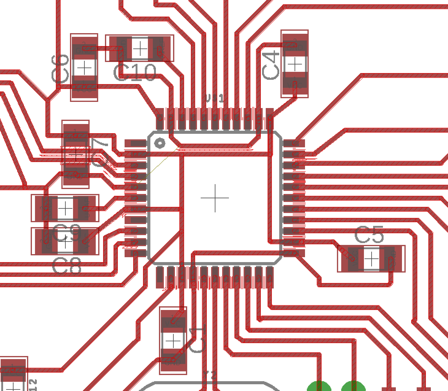
I used Luiz’ board to get the basic BOM and pin connections for the ATMega32U4
I then tried to map out all the different systems I’d need on the board, and the parts for each, mapping these, where appropriate against Luiz’ board.
Pin connections for current smoothing over VCC and GND pins.
I copied all of these from Luiz’ board.
VCC Pins:
- 14 / VCC2
- 34 / VCC
- 2 / UVCC
- 24 / AVCC_2
- 44 / AVCC
all connected via 0.1uF capacitors to
GND pins:
- 15 / GND_2
- 23 / GND_3
- 35 / GND_4
- 43 / GND
- 5 / UGND
Also
- 7 / VBUS
- 6 / UCAP
- 42 / AREF
all connected via 0.1uF capacitors to common ground
After doing some research into these decoupling capacitors, I decided to place them as close as possible to the IC.
From: https://learn.sparkfun.com/tutorials/capacitors/application-examples
When physically placing decoupling capacitors, they should always be located as close as possible to an IC. The further away they are, they less effective they’ll be.
Reset pin
Again, I wasn’t sure how to use this, or how it had been connected on the board I was basing my design on.
From https://www.eevblog.com/forum/beginners/is-it-ok-to-leave-atmega328p-reset-pin-floating/
If you don’t need the reset pin function, you could program the fuses so that it’s not a reset pin anymore. Then you won’t need an external pullup and you’ll also have another gpio pin that you can use. You can still reset via a power cycle.
From the data sheet:
PC6/RESET
If the RSTDISBL Fuse is programmed, PC6 is used as an I/O pin. Note that the electrical characteristics of PC6 differ from those of the other pins of Port C.
If the RSTDISBL Fuse is unprogrammed, PC6 is used as a Reset input. A low level on this pin for longer than the minimum pulse length will generate a Reset, even if the clock is not running. Shorter pulses are not guaranteed to generate a Reset.
I’m going to use it as a reset pin, as i think this functionality could be useful, and I don’t need any more IO pins right now. Again, some more research:
When adding an external pull up resistor (say 1 to 10kohm) a small capacitor (1nF or 10nF ceramic) between reset and ground can help improve EMI/EMC performance; meaning less “unexplained” resets.
From: https://programmingelectronics.com/how-to-use-an-external-reset-button-with-arduino/
So just what is happening in this circuit – and why would this circuit work anyhow? According to the Arduino web page… “ In addition, some pins have specialized functions: – Reset. Bring this line LOW to reset the microcontroller. Typically used to add a reset button to shields which block the one on the board.” So all we have to do is bring the pin LOW – which is as easy as connecting it to ground through a pushbutton. So when the button is not pressed, the pin is in its normal state. When the pushbutton is pressed, the pin “sees” ground voltage (i.e. 0 volts), and is brought LOW – which according to the documentation will reset the Arduino for us.
So in my design I’ll use a 10k0 resister from Reset to VCC, and also bridge this to GND with a 10nF (0.01uF) capacitor, and add a button (bridging RST to GND) to manually reset too.
Timing
I’m using a 16MHz Crystal, rather than the resonators we’ve used in previous boards
- One side connected to 17 / XTAL1
- And via 18pF capacitor to GND (common) (all 1206 packages)
- Other side connected to 16 / XTAL2
- And via 18pF capacitor to GND (on USB port
This must all be symmetrical in the layout,
The reset and timing parts on my board layout:
Status LED
Another nice-to-have feature, an LED on the ‘D13’ pin, the equivalent of the built-in LED on the Arduino.
- LED (1206 package), connected to PC7(ICP3/CLK0/OC4A) / 32 / D13 via 500Ohm Resistor, then sent to the common GND trace
Spare pins and I2C Communication
Luiz suggested I should try to connect the remaining IO pins to headers so I could access these later if necessary. As I’m hoping to test out using a PISO shift register to collect inputs from my array of switches, this could be useful later on.
Group 1 (bottom right corner):
- 18 SCL (for I2C)
- 19 SDA (for I2C)
- 20 PD2/RX
- 21 PD3/TX
- 22 PD5
Group 2:
- 41 PF0 (ADC0)
- 40 PF1 (ADC1)
- 39 PF4 (ADC4)
- 38 PF5 (ADC5)
Isolated pins (I won’t take these out to headers):
- 12 PB7 (Bottom left corner)
- 8 PB0(SS) (mid left)
- 1 PE6 (top left)
USB Port for programming, communication and power
Connected as follows:
- GND to common GND
- VBUS to 7 / VBUS
- D- via 22O Resistor to 3 / D-
- D+ via 22O Resistor to 4 / D+
ISP Programming header
2x3 header connected to:
- MISO
- SCK
- RST
- VCC
- MOSI
- GND
Parallel input from multiple switches via header (for 10 switches)
And finally, the main point of my board – a long header to accept inputs from an array of 10 switches:
- 20x1 header - (I’m actually using 2 x 1x10 male headers as they have the correct pin spacing)
- 10 x pins connected to 10k pull down resistor to GND, also connected to digital input pins on Atmega
- 10 x pins connected to VCC
- 10 x 10k resistors - 1206 Package
Milling my board
I had to reduce my trace widths to 12mil (0.3mm) to ensure clearance between some of my pads. I also had to use a 0.3mm drill bit on the Roland MDX-50 as some of the spaces were so tight. The board milled OK in the end, despite the fact that the bit we thought was 0.3mm, was actually 0.4mm, resulting in some very thin traces.
After milling, I noticed some problems with some of my traces connecting, so we cut these shorts with a craft knife.
I also noticed a few problems, with some of my pads that I should address in a future version of this board.
- The pads for the crystal do not match the crystal packages we have. I should check for the correct package in Eagle.
- Some of the pads could be more generous, allowing for easier soldering
- The 20x header has the correct pad size for the male headers we have. My smaller 5x and 4x headers have pads which are too small.
- The pads for the feet of my USB port don’t quite match the feet of the USB ports we have
- My UBSB port is too far away from the edge of the board to allow a USB cable to be plugged in.
- Could I place my D13 LED somewhere else on the board to require fewer traces running underneath components?
- Do I need those pull-down resistors on my switch inputs?
### Soldering
I had a lot of problems with my traces shorting and delaminating from the board.
I also noticed that my USB port is too far from the edge, so had to drill away parts of the board to allow me to plug in a USB cable.
I left one of my traces broken on the GND loop (to see if I could get it to work anyway), and also tried using some 0Ohm resistors on 3 of my input pins to see if I can test out using internal pull-down resistors on these pins instead. If that works, I could get rid of the hardware resistors on the board, making it much simpler to route traces.
Burning the bootloader and a test sketch.
I followed the instructions here to burn a bootloader for the board as an Arduino Leonardo, using my FabISP as the programmer, then uploaded the Blink sketch as a basic test. This all worked first time.
However, when I removed the FabISP, and tried to program the board directly, the Arduino IDE wouldn’t recognise the board. It turned out there were multiple problems with the connections from the USB port. With Luiz’ help, we removed the capacitor bridging two of these traces
We also checked for shorts and poor connections on the USB port, and repaired these with solder and bridging wires.
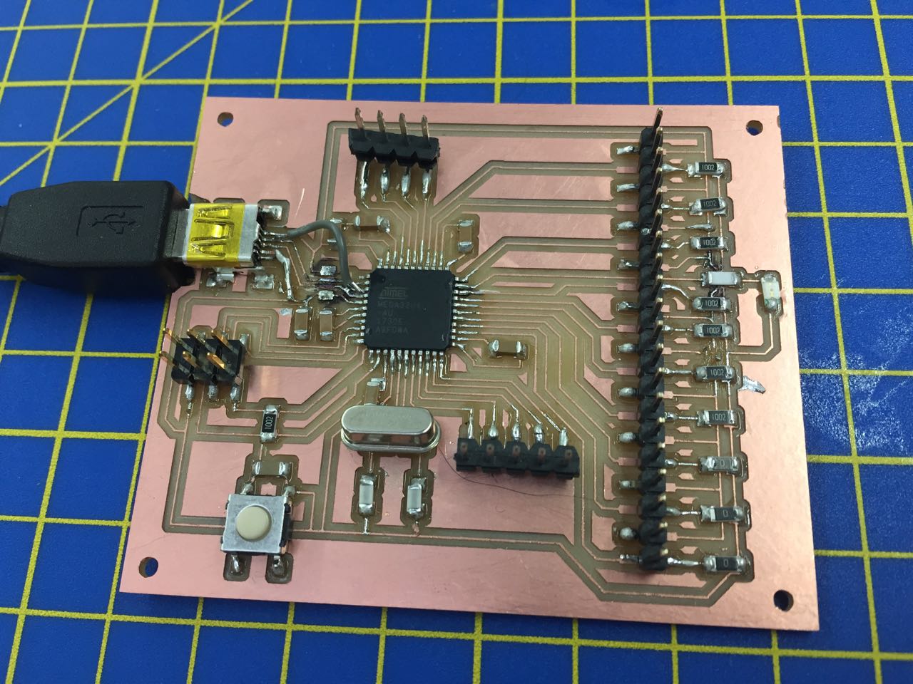
After this, I was able to program the board directly through the USB port.
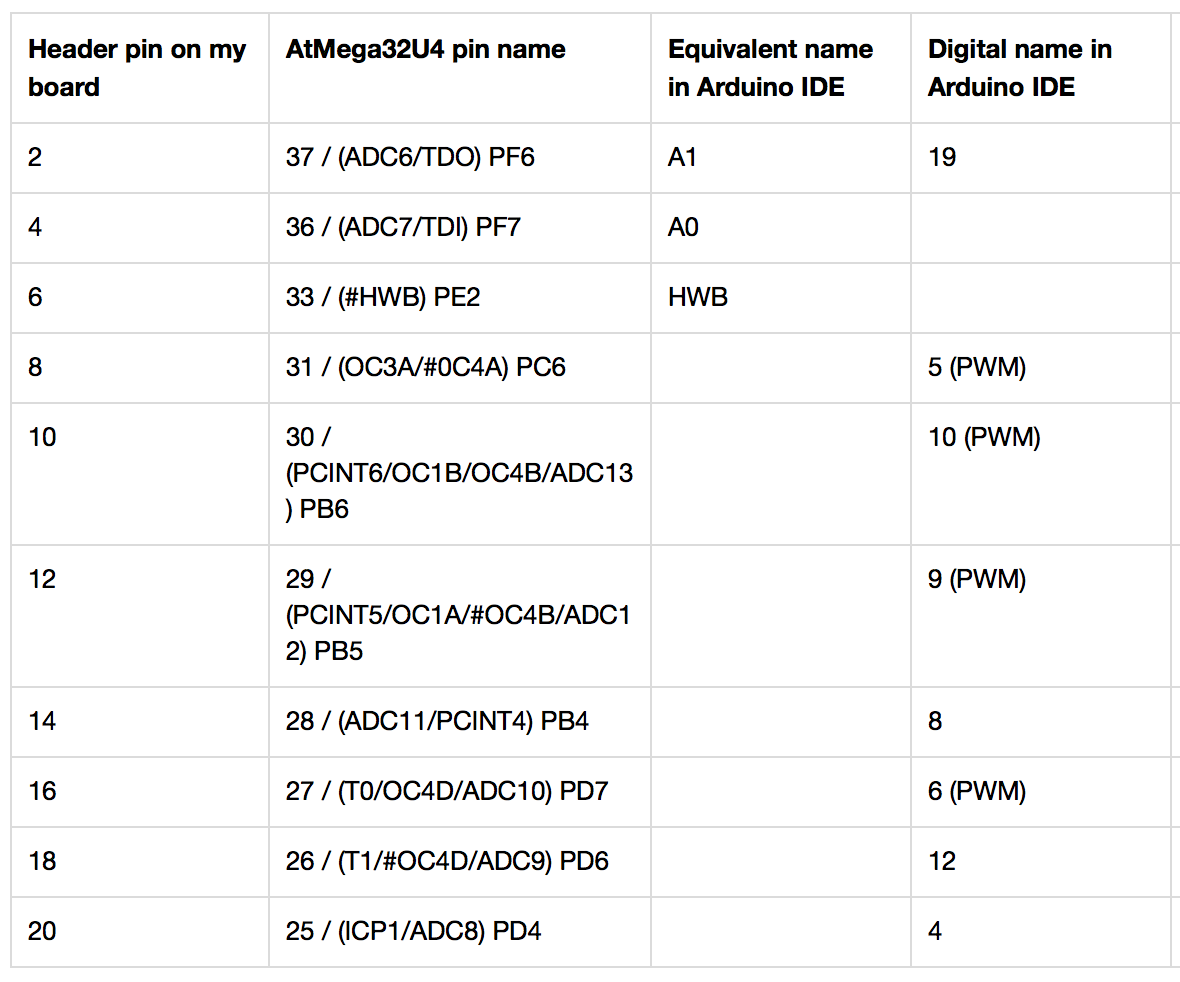
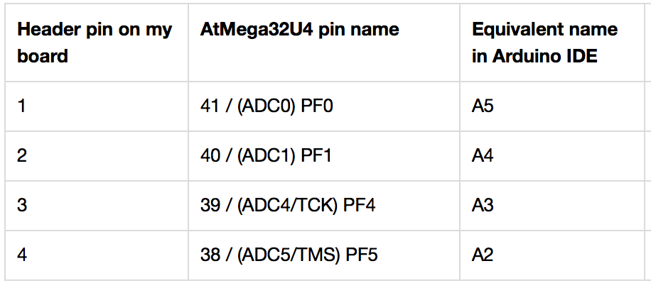
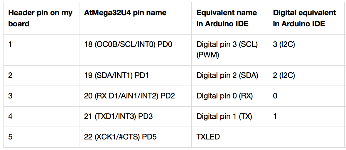
Testing the input pins
Using one of the ATMega32U4 pin mapping tables, I made mapping tables of all my exposed pins to the pin numbers that the Arduino IDE expects.
My 20 pin header (top - bottom with header to right of chip)
My 4 pin header (L-R with header above chip)
My 5 pin header (L-R with header below chip)
This board had many flaws, which I went on to fix in a modified version for next week’s assignment, however, I was able to wire up buttons to my 20 pin header and read their input.
For a complete input demo, continue reading my Output Devices assignment