Assignment 8:- Electronic Production
Learning outcomes
in this week i learned about the electonic production and how to make the pcb board and how to solder the components on the pcb board and how to make the circuit and how to tesr the crcuit and how to make the pcb borad using the software and how to make the flexiable pcb board using vinayl cutter. i also lerining about thr DRC and ERC rules. To learn how to use SRM-20 milling machine to make a PCB board.
Hero shot
This week Assignment Task
Group assignment:
Characterize the design rules for your in-house PCB production process: document the settings for your machine.
Document the workflow for sending a PCB to a boardhouse.
Document your work to the group work page and reflect on your individual page what you learned.
Individual assignment:
Make and test a microcontroller development board that you designed
Group Assignment
in this week we have to make the pcb board milling mechince and we have to Characterize the design rules for our pcb and we have to document the process of our mechine.
In this week lerning about the milling mechine and how to make the pcb board using the milling mechine. as a group assinment i have to cut the pcb borad using the milling mechine. lerining about the DRC and ERC rules and how to make the pcb board using the software.
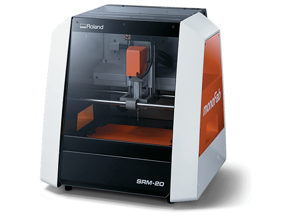
In our lab we have the SRM-20 milling mechine and we havr to make the pcb board using the SRM-20 milling mechine.
Our mentor teach us how to usr the srm-20 milling mechine and mechine sefty rules . explaing the how to genreting the tool path for the pcb board and how to set the parmeters for the milling mechine and how to cut the pcb board using the milling mechine.
i document the process of cutting the pcb. in this process i have to set the parameters for the milling mechine and cutting the test file provided by the fab academy and after cutting the pcb board we have to conclusion the characterization of the milling mechine.
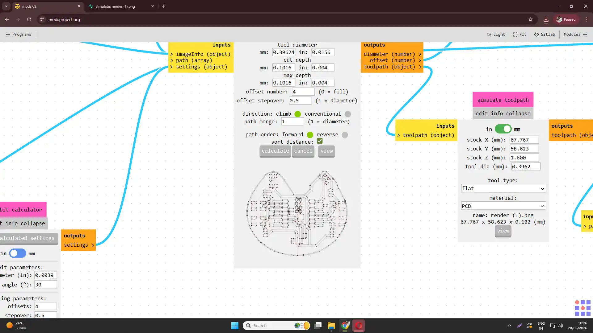
For the group assigment grenating the tool path.
we have to 1st downlaod the test file provided by the fab academy and we have to use the mood software to generate the tools path for the pcb milling and Cutting the pcb.
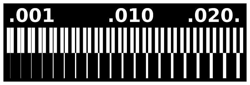

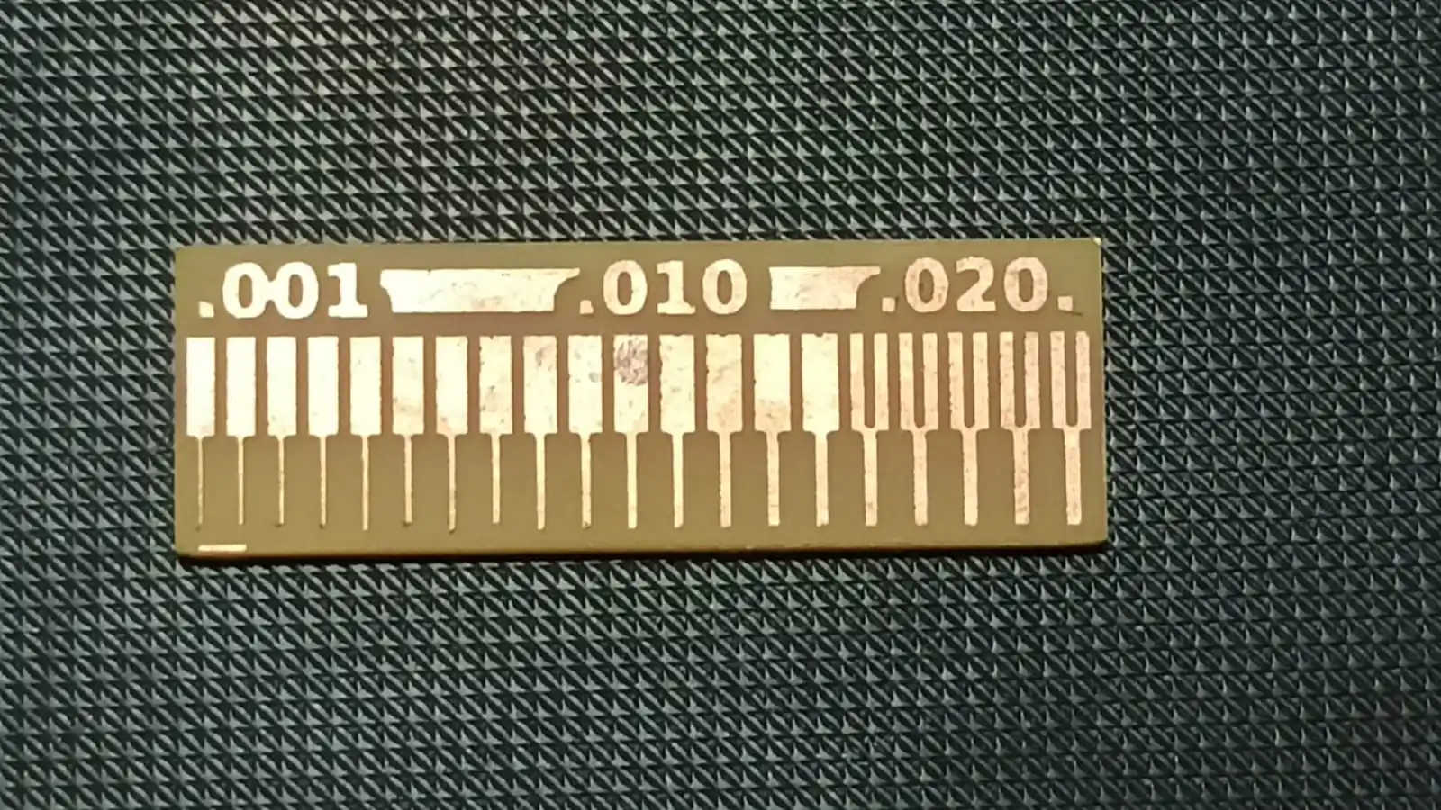
this file is the test for the milling mechine acuracy and we are use the 1/64 inch end mill for engraving and 1/32 inch end mill for the cutting the pcb board.after cutting the pcb board we have to conclusion the characterization of the milling mechine.
Conlcusion
1) 1/64 bit mile fine trace accurate .
2) Medium and wider traces (0.010 and 0.020 inch) are milled more clearly and accurately.
3) 1/64 inch bit works well for PCB milling, but for best results, we should avoid very thin traces and follow proper design rules and machine settings.
4)Conclusion (DRC): Design Rule Check (DRC) is a crucial step in PCB design that ensures the layout adheres to specific manufacturing constraints and standards.
It helps identify potential issues such as spacing violations, trace width problems, and component placement errors. By performing DRC, designers can ensure that their PCB design is manufacturable and will function correctly, reducing the risk of costly errors during production. In our PCB milling process,
we followed DRC guidelines to ensure that our design was compatible with the capabilities of our milling machine and met the necessary requirements for successful fabrication.
Maintain minimum trace width ≥ 0.010" for standard designs
Click Here Group Assignment Electronic Production
Individual Assignment
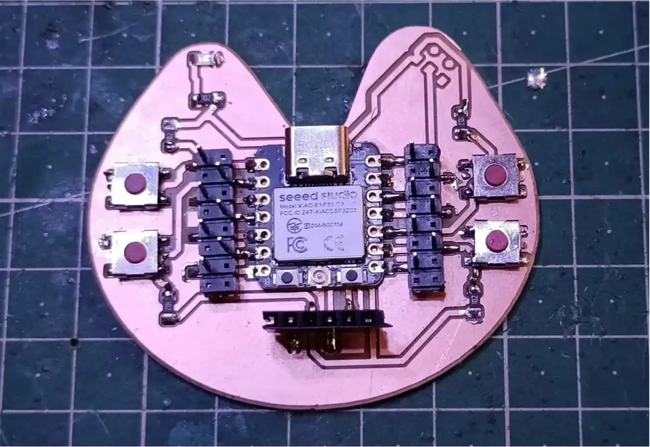
During this week, the assignment was to design and fabricate a microcontroller development board. The process included PCB design, PCB fabrication, component soldering, and testing of the final board.
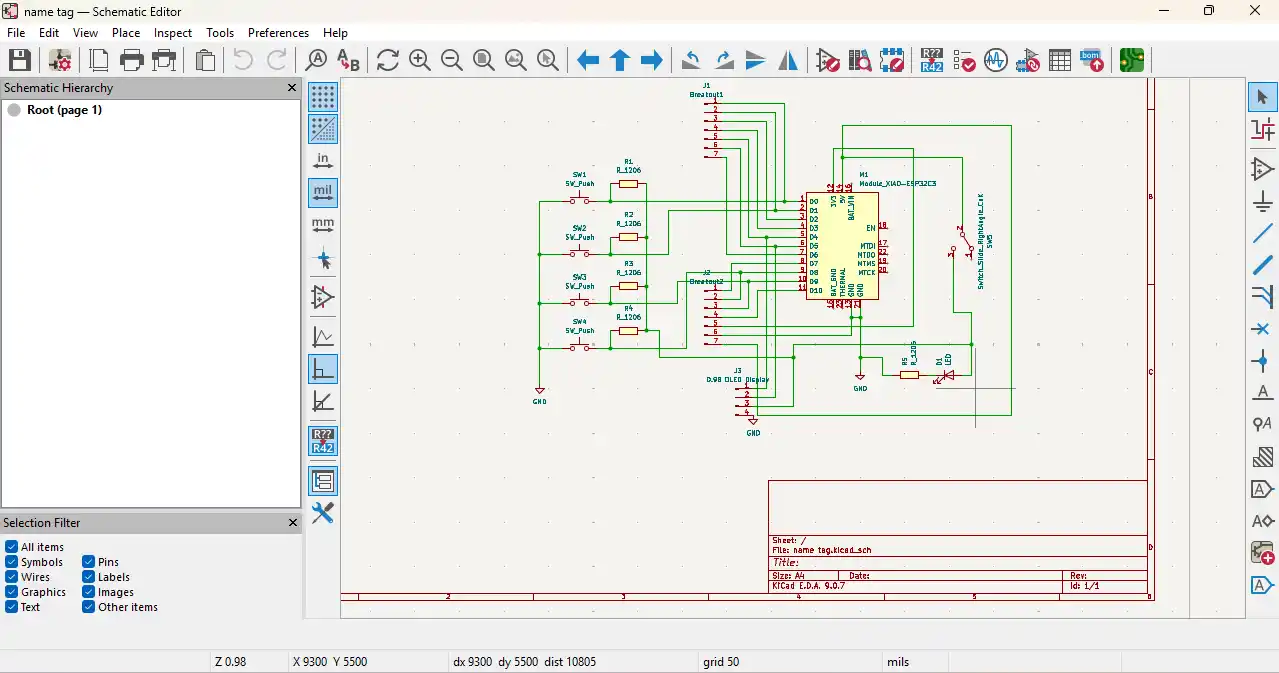
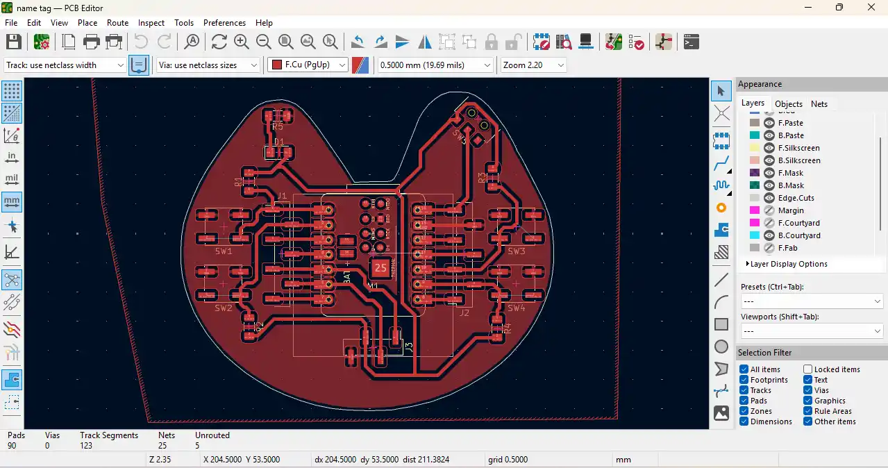
I initially designed the PCB during the Electronics Design week using KiCad software. However, the original design used through-hole components, which were not suitable for the PCB milling process. Since the milling machine requires SMD components, I redesigned the PCB using surface-mount components.
The redesigned PCB was fabricated using a milling machine. After fabrication, the electronic components were soldered onto the PCB, and the board was tested to verify proper functionality. The complete workflow and documentation here.
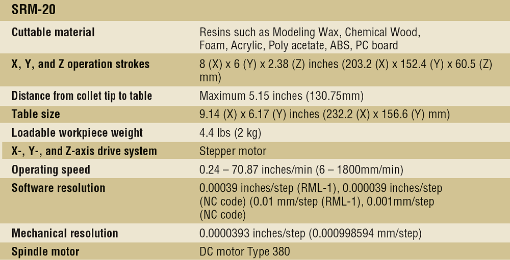
SRM-20
In our lab, we use the MonoFab SRM-20 desktop milling machine for PCB fabrication and molding applications. The machine is capable of milling and cutting PCB boards, as well as machining machinable wax for mold making. VPanel software is used to control and operate the machine.
.png)
Reference links
Required tools
During the pcb milling process, i use the following tools and materials:
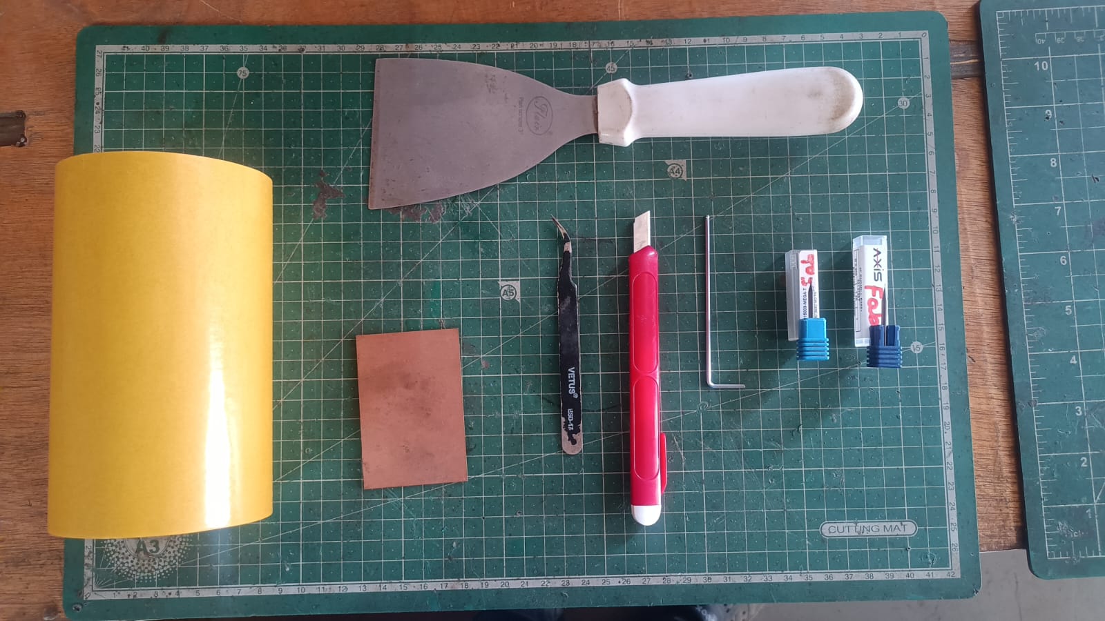
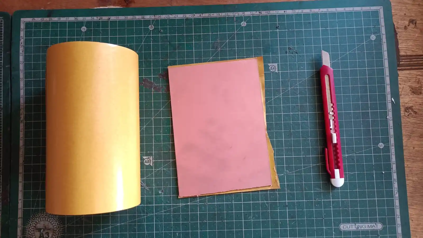
1) Copper clad single side pcb board.
2) 1/64 inch end mill for engraving.
3) 1/32 inch end mill for cutting the pcb board.
4) double sided tape for fixing the pcb board on the milling bed.
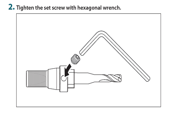
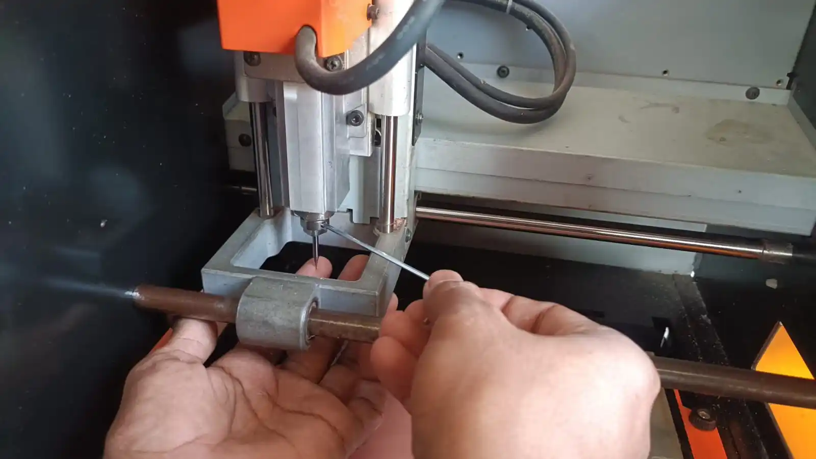
5) Alen key for the chenging the end mill bit.
6) Spatula for removing the pcb boabd from the milling bed.
Tool setup and sefty rules
Before starting the milling process, it is important to set up the tools properly and follow safty rules to ensure a successful and safe operation. Here are the key steps for tool setup and safety:
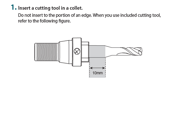
1) tool setup:
-Install the appropriate end mill bit (1/64 inch for engraving and 1/32 inch for cutting) securely in the spindle of the milling machine.
Reference links
-Ensure that the end mill bit is properly tightened using the appropriate tools, such as an Allen key, to prevent it from coming loose during operation.
-Secure the copper clad pcb board onto the milling bed using doule side tape to prevent any movement during the milling process.
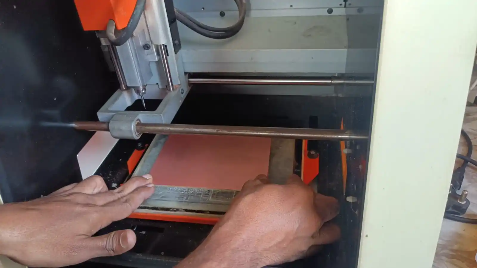
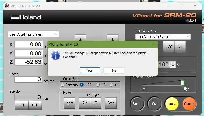
Set up the origin point for the milling mechine using the v panel software to ensure accurate milling of the pcb board.
origin point is the referance point for the milling process and it is important to set the origen ponit [x,y,z] correctly to ensure that the milling pocess is accurate and the final pcb board is milled correctly accordiing to the desgin file.
.webp)
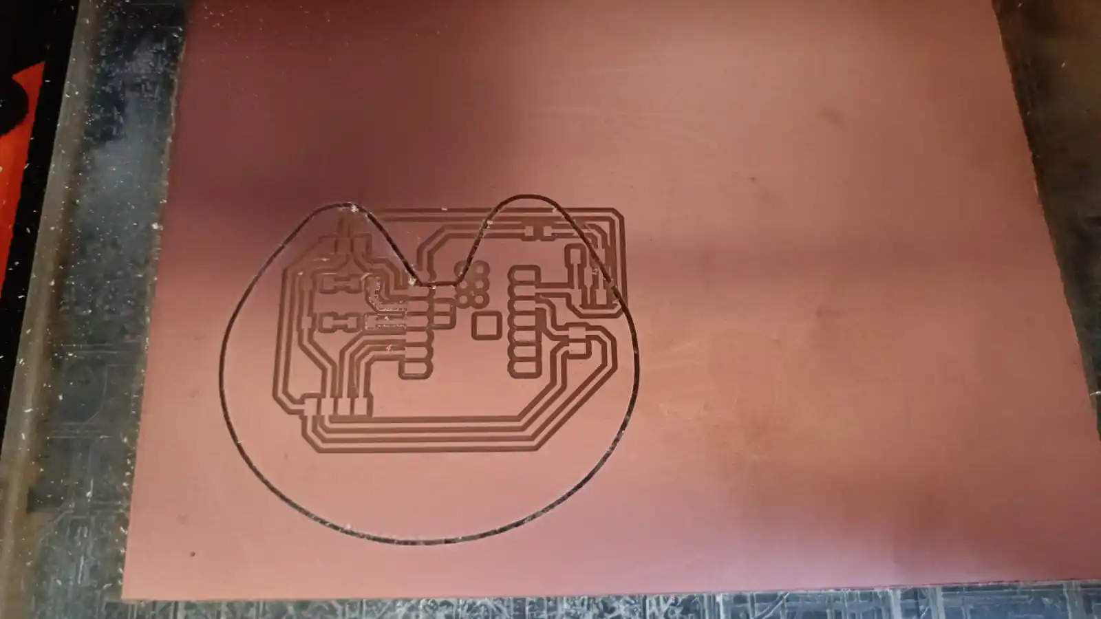
In the next step make file ready for the milling pocess. so this my update file for shematic and pcb design this file design in kicad software and after making the file ready for the milling process i have to generate the tool path for the milling process using the mood software and after generating the tool path.
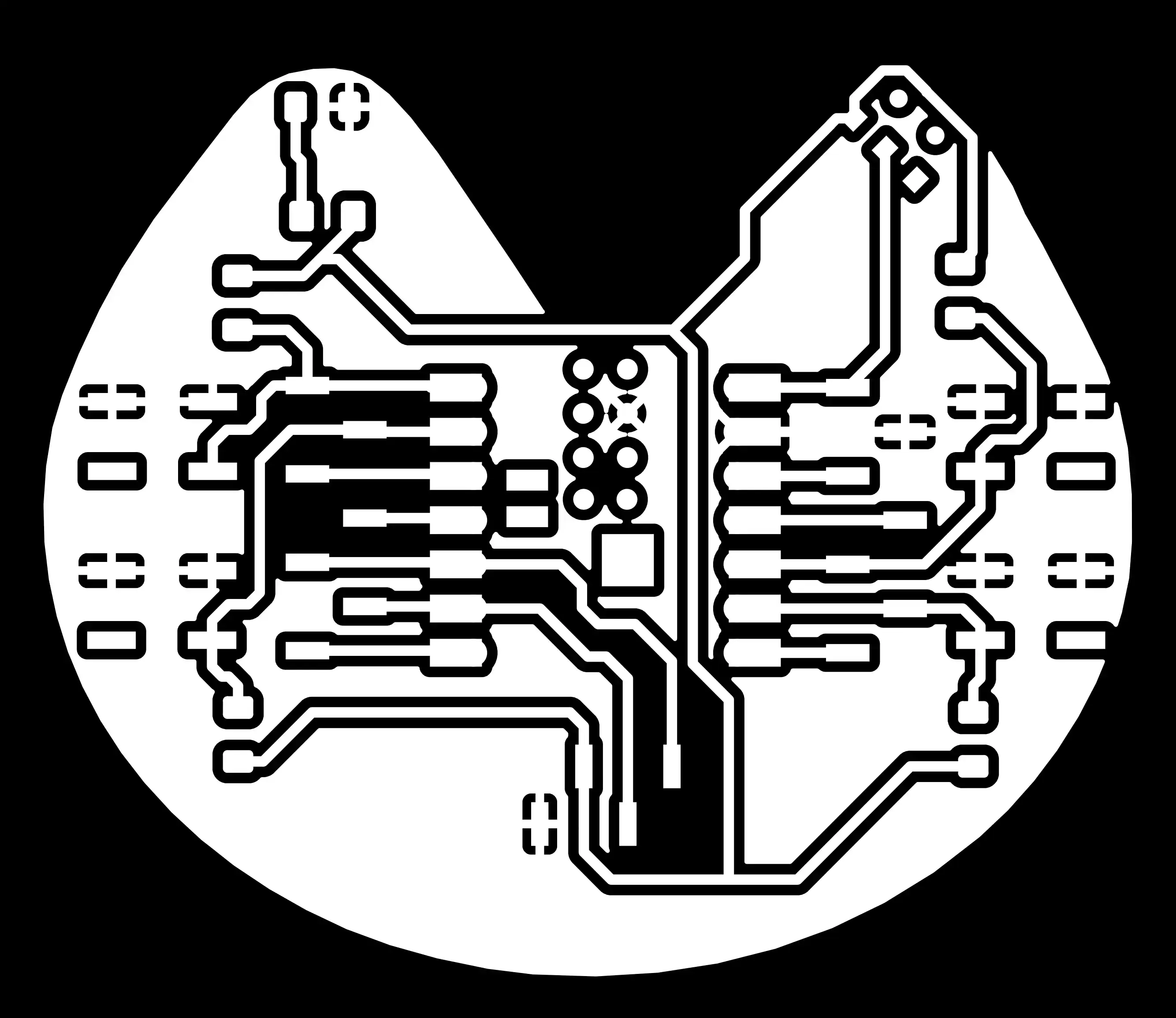
After that this file coverted in the gerber filr and after that this file agin coverted gerber file to png file using the gerber2img online converter.
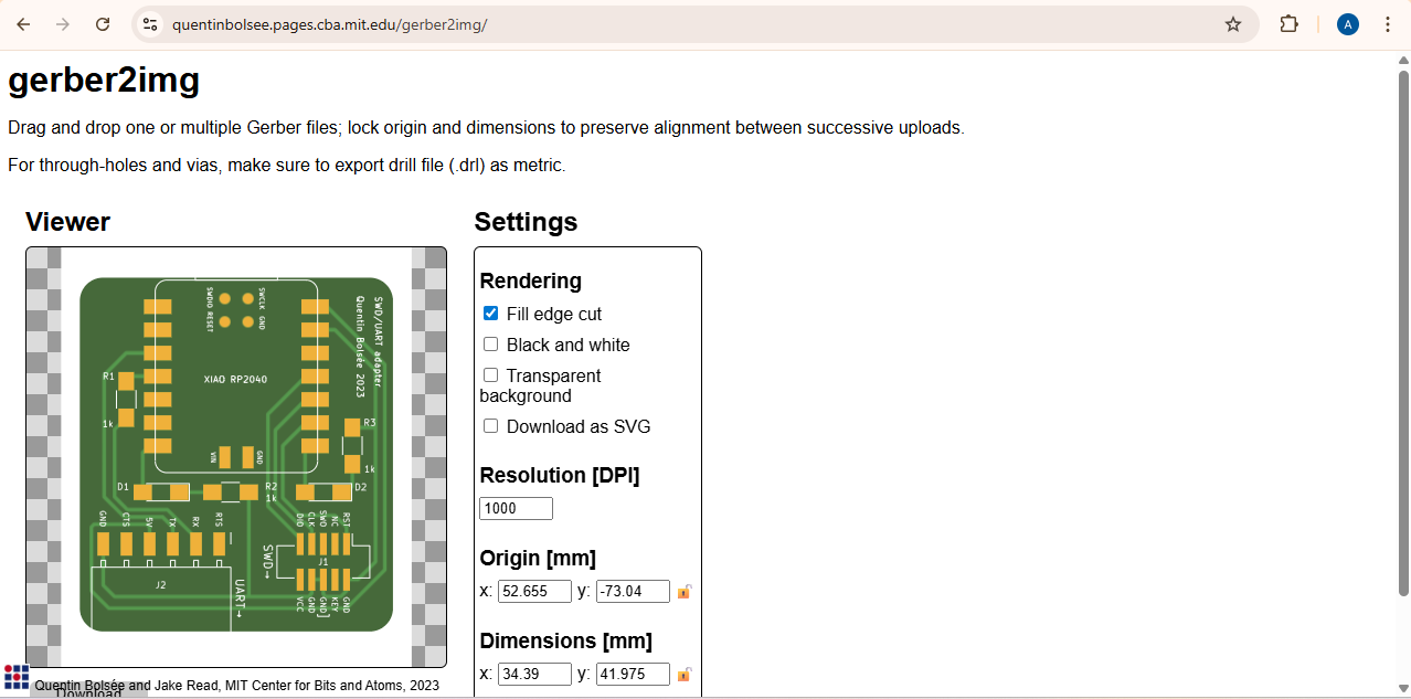
gerber2img
These are the PNG files generated for PCB fabrication. I created two separate files: a trace PNG file for milling the PCB traces and an edge-cut PNG file for cutting the board outline. These files are imported into the Mods software to generate the toolpaths for the final milling process.

In next i will go on the mods software to generate the tool path for the milling process to flow the this steps.
mods
1) open the mods software select the mechine and import the trace PNG file to generate the tool path for milling the PCB traces.
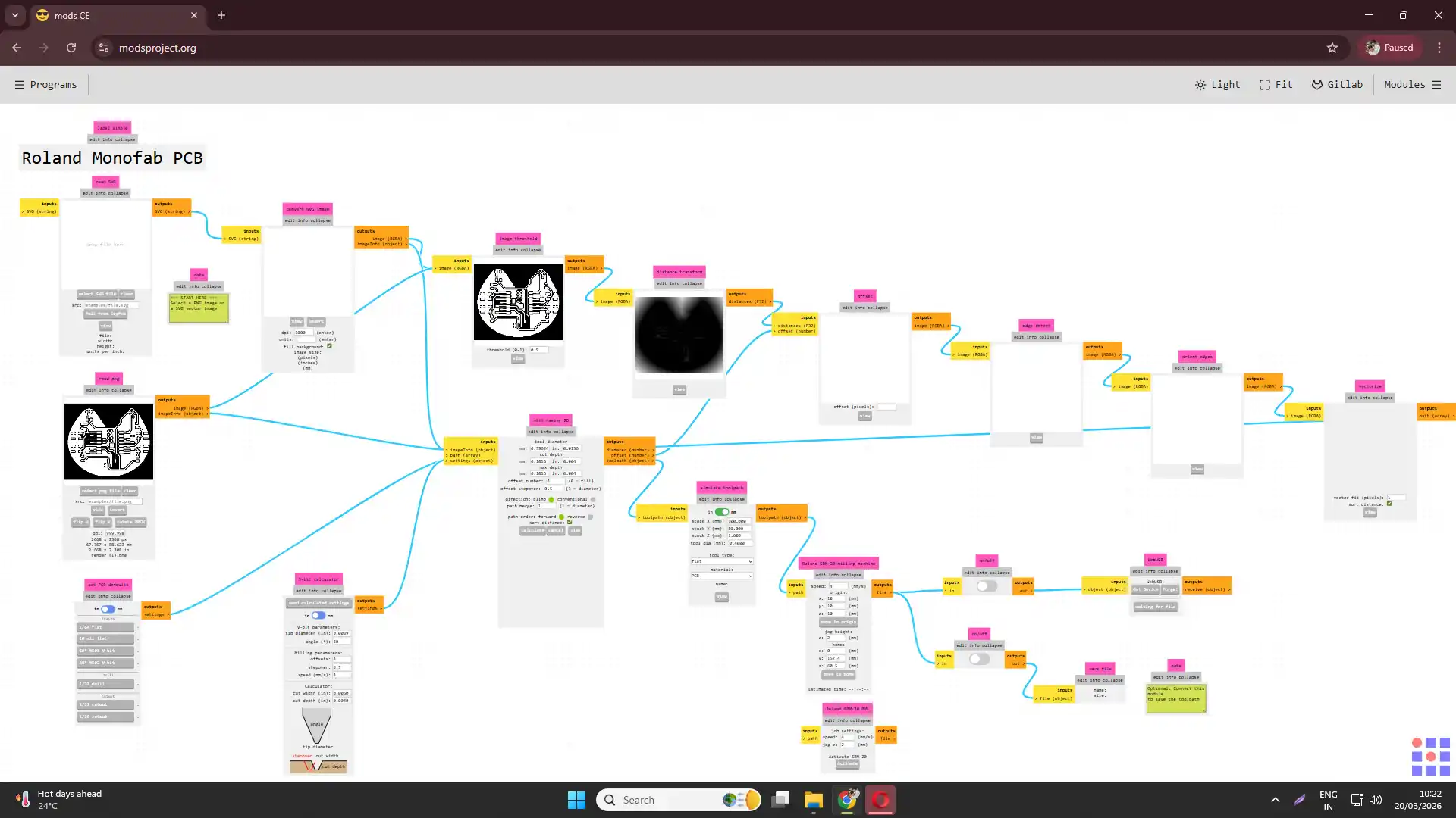
2) set the appropriate parameters for the milling process, such as feed rate, spindle speed, and cutting depth, based on the material and the end mill bit being used.
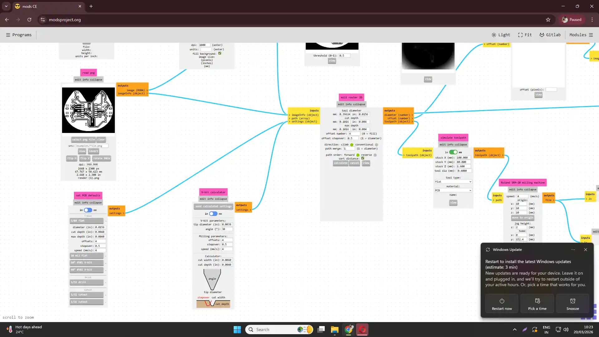
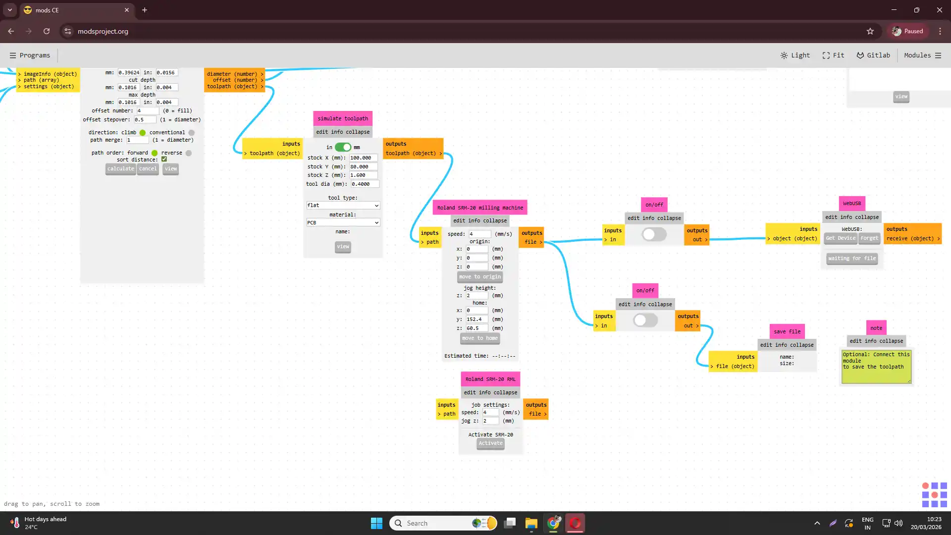
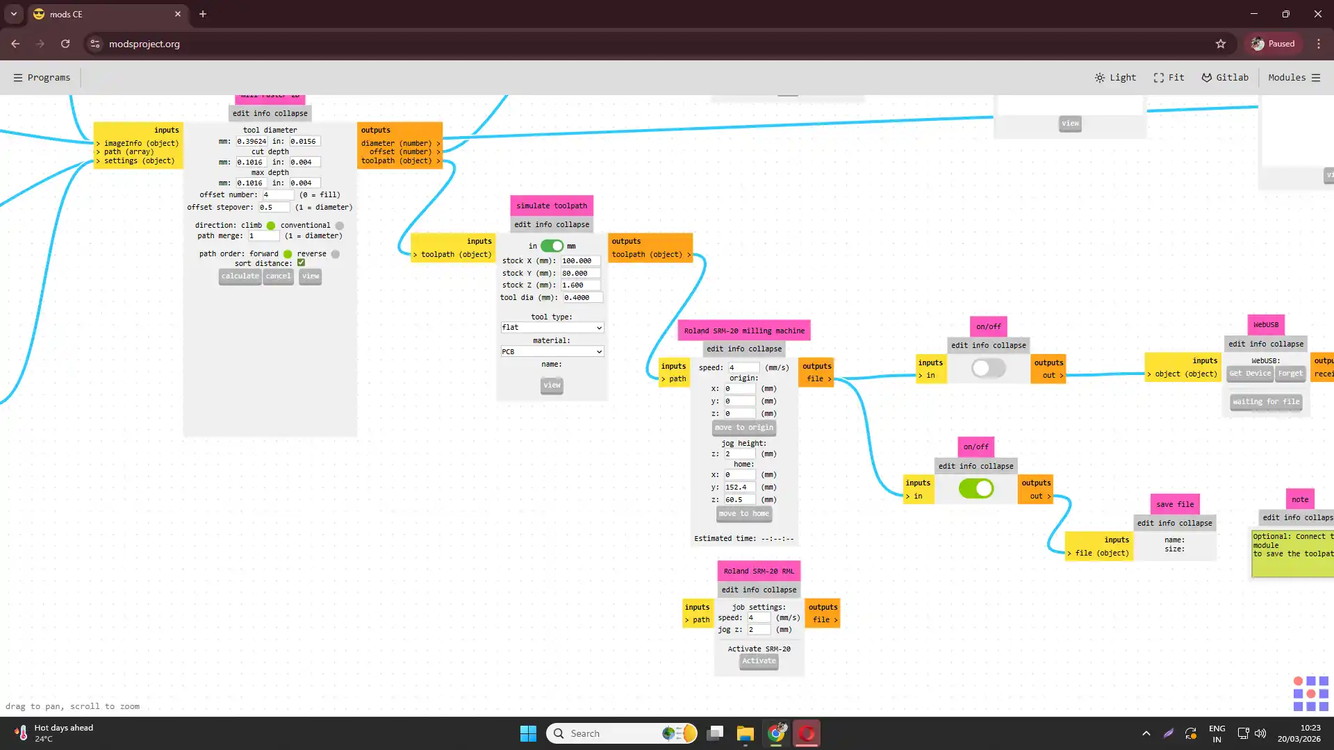
3) generate the tool path for milling the PCB traces and save the file.
4) repeat the process for the edge-cut PNG file to generate the tool path for cutting the board outline, ensuring that the parameters are set correctly for cutting through the entire thickness of the PCB material.
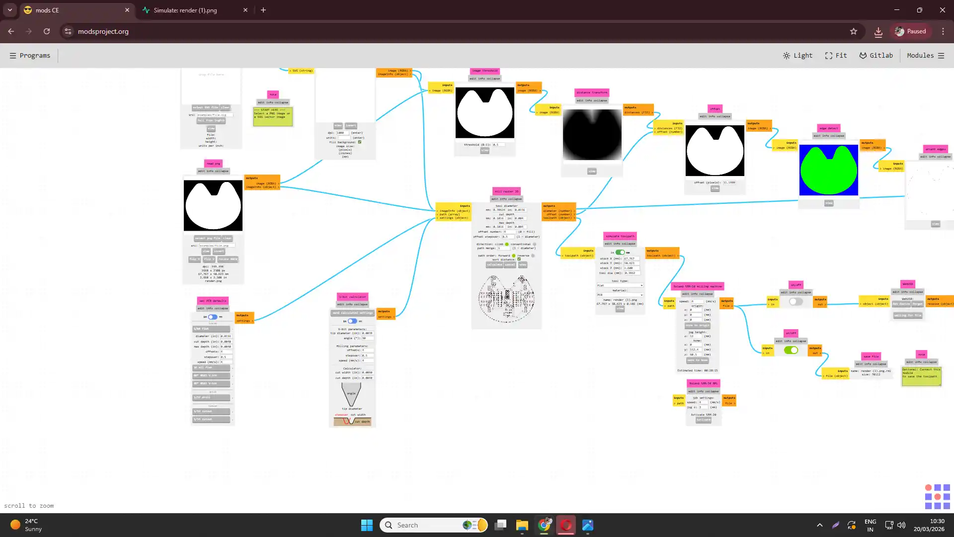
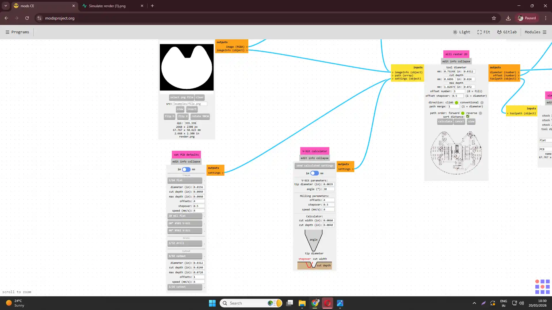
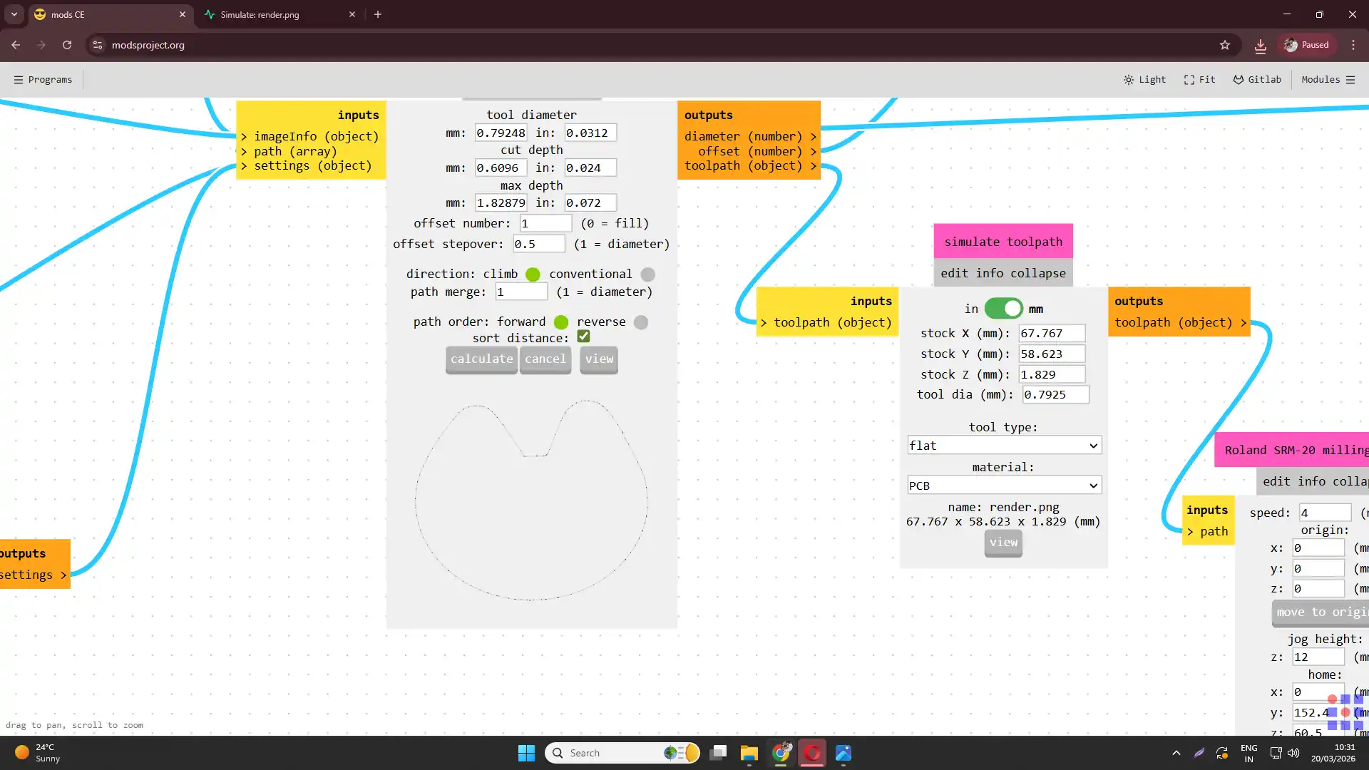
5) After generating the tool paths, load the files into the VPanel software to control the milling machine and start the milling process.
.webp)
.webp)
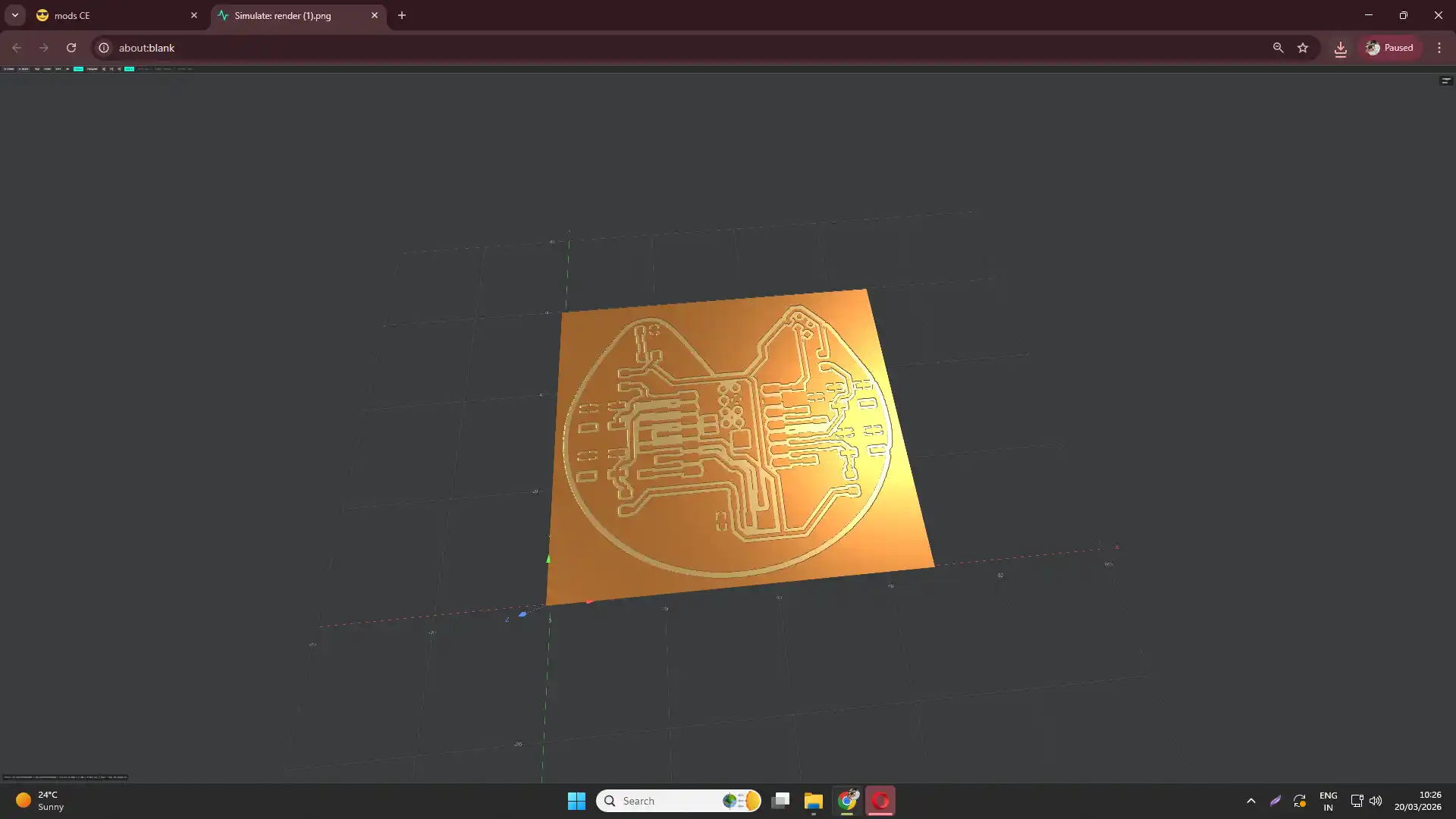
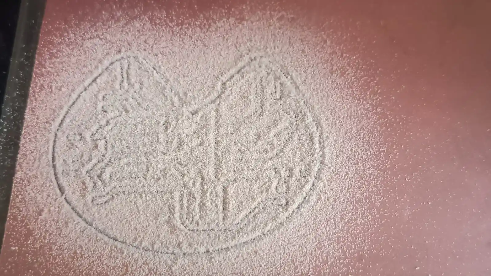
After milling the PCB board, all the dust was cleaned using a vacuum cleaner. The PCB board was then checked for any defects or issues, such as incomplete traces or rough edges. Necessary adjustments were made to the design or milling parameters for future iterations.
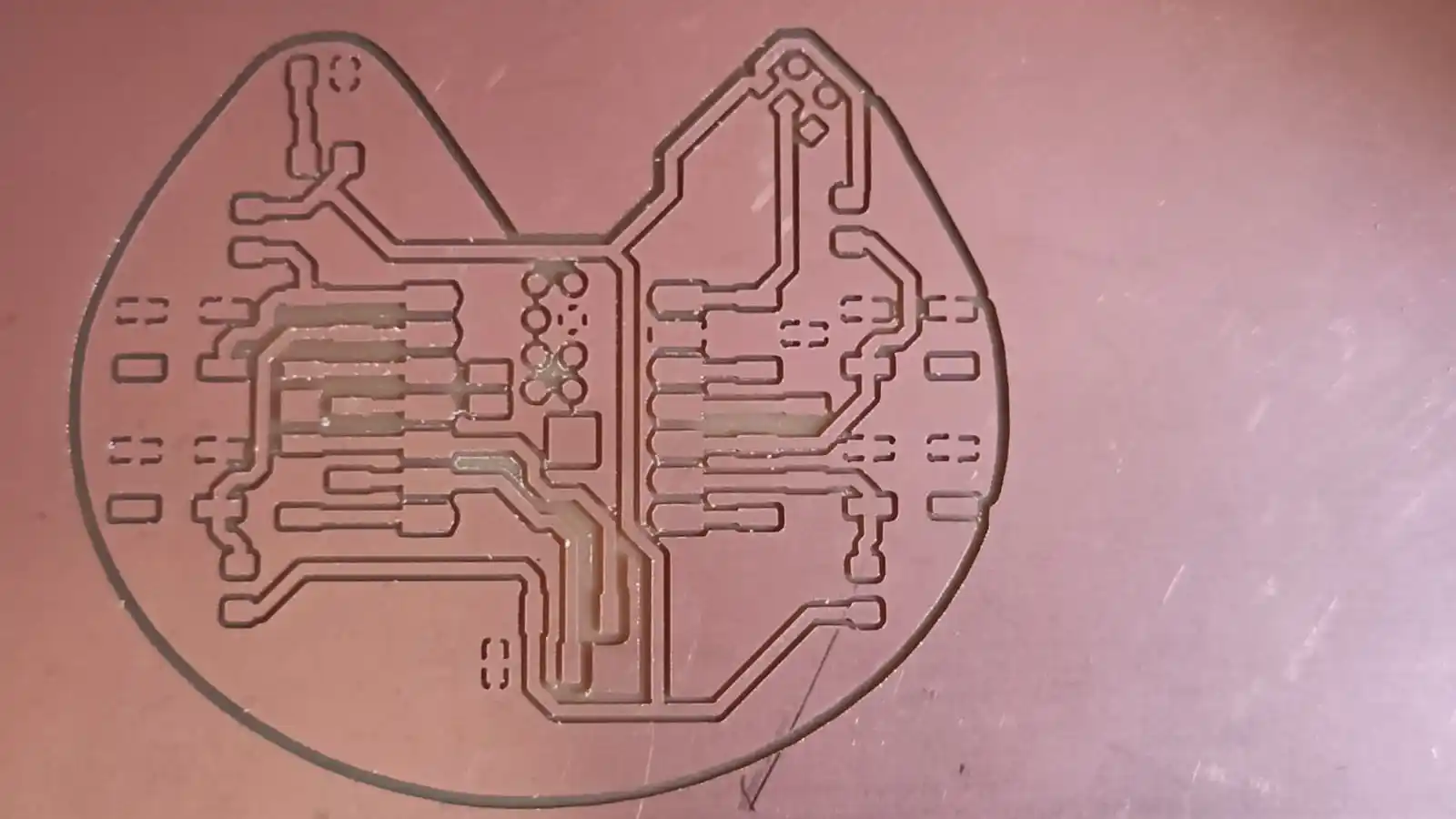
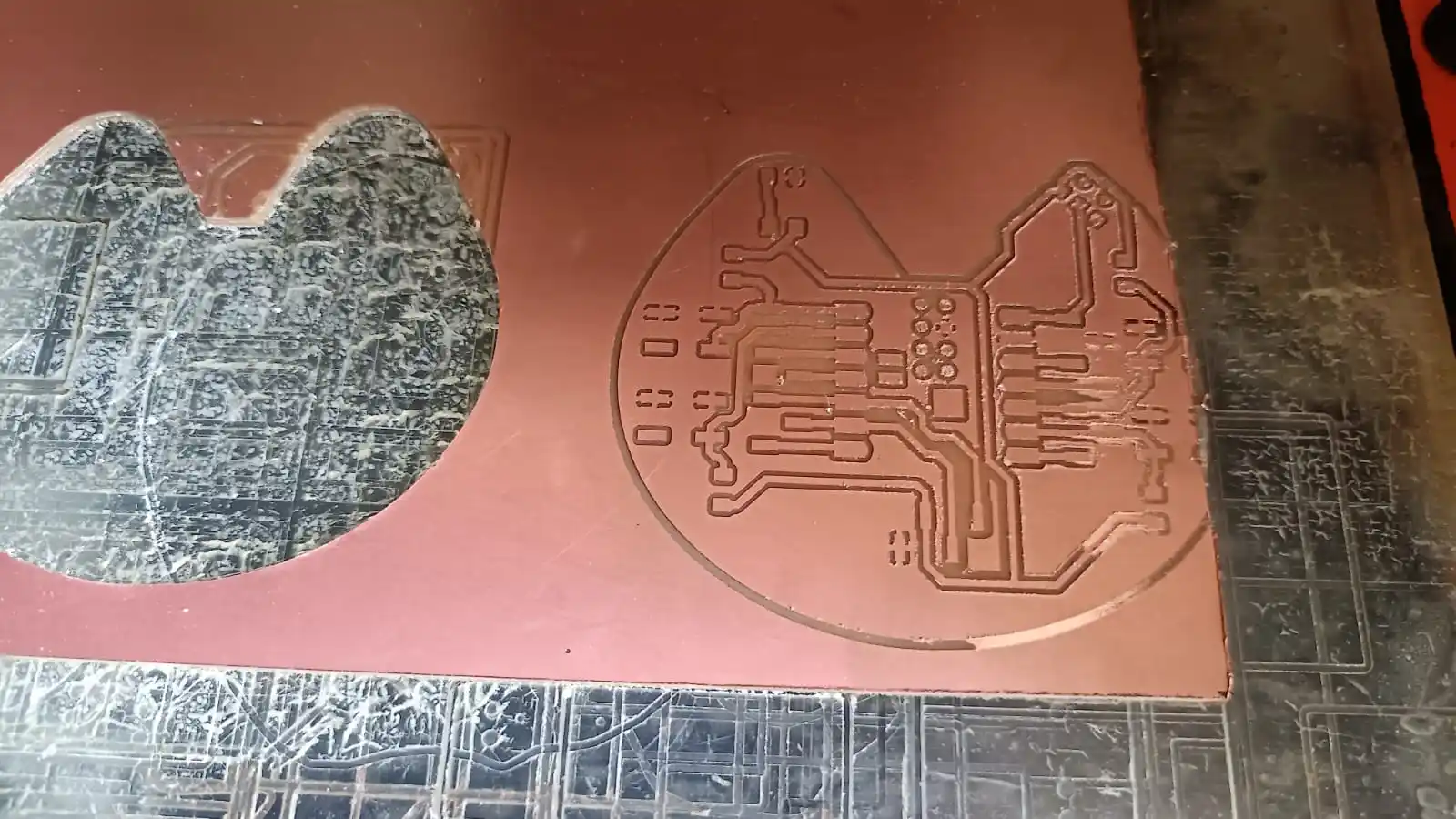
6) After that the again same process but chenge the bit for cutting the pcb board using 1/32inch end mill.
Monitor the milling process closely to ensure that the machine is operating correctly and that the PCB is being milled accurately according to the design specifications.
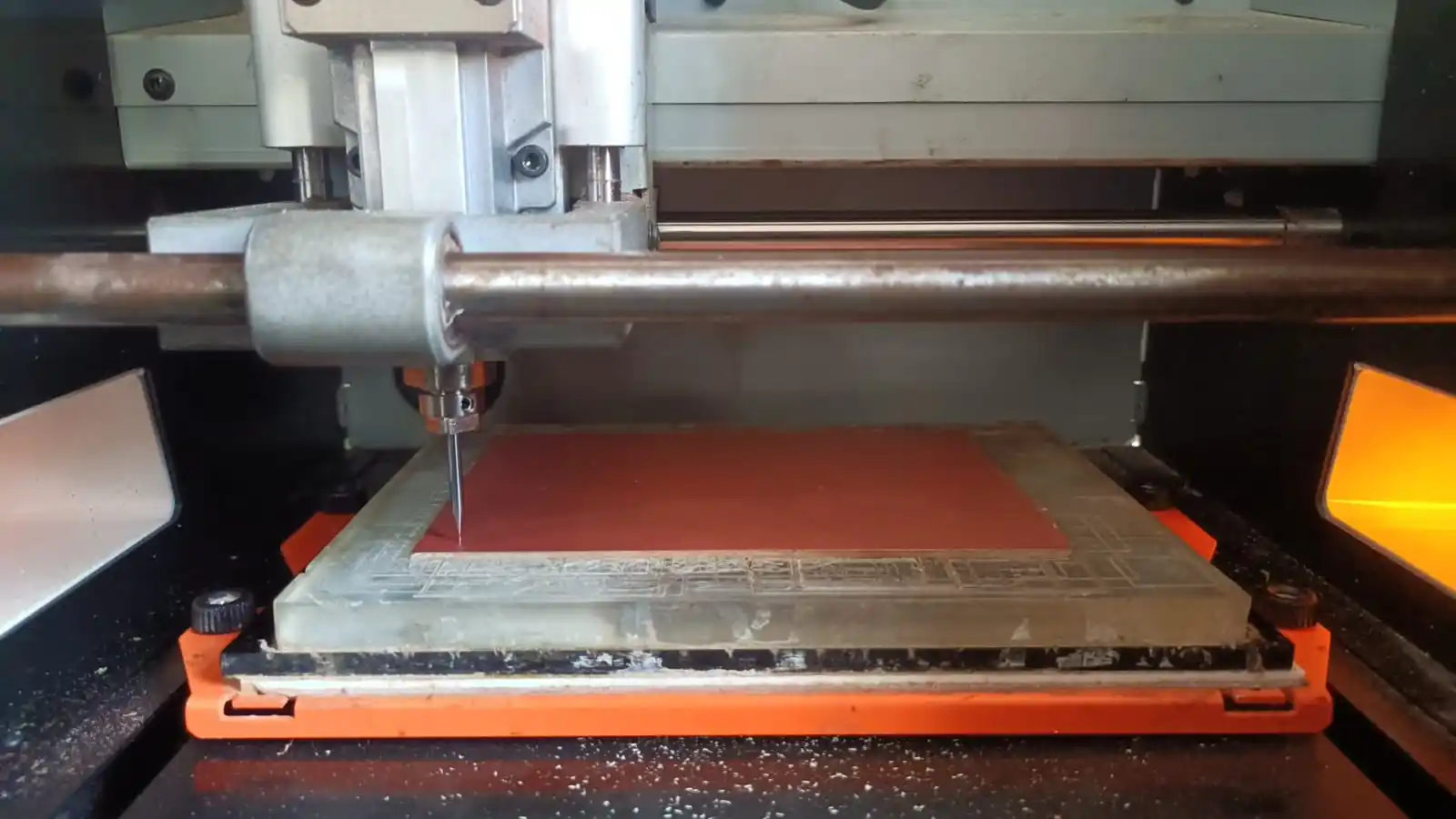
After milling the PCB board, all the dust was cleaned using a vacuum cleaner. The PCB board was then checked for any defects or issues,here finlly the pcb board is milled and ready for the soldirng it looks like.
7) Once the milling process is complete, carefully remove the milled PCB from the milling bed using a spatula or similar tool, taking care not to damage the board.

8) Inspect the milled PCB for any defects or issues, such as incomplete traces or rough edges, and make any necessary adjustments to the design or milling parameters for future iterations.
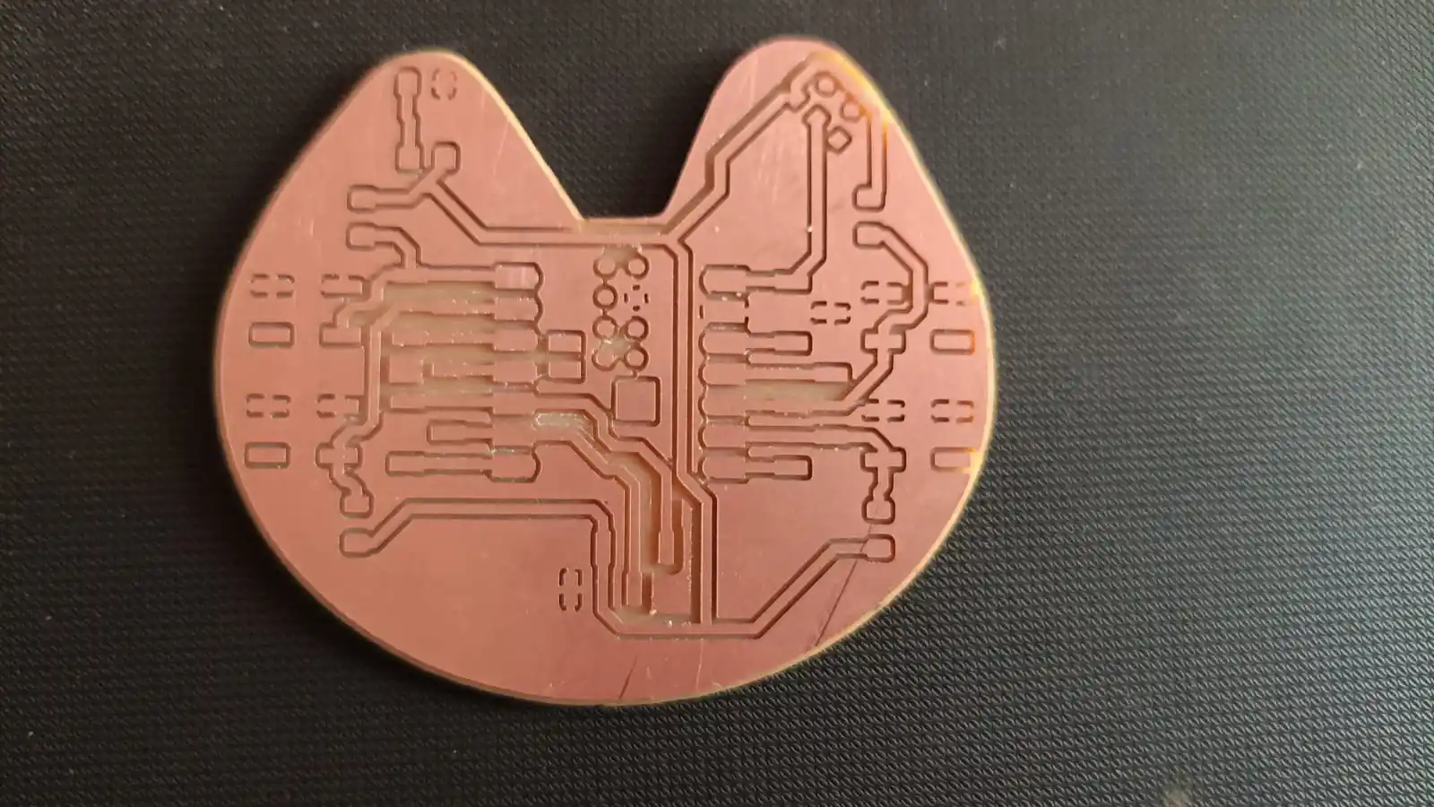
9) Finally, proceed with soldering the components onto the milled PCB. and testing the final board to ensure it functions as intended.
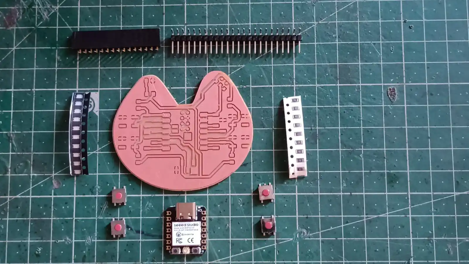
In this my pcb i use xiao esp32 microcontroller and led and resitor and push button and hidder pin to conntected for the oled disply and other components.
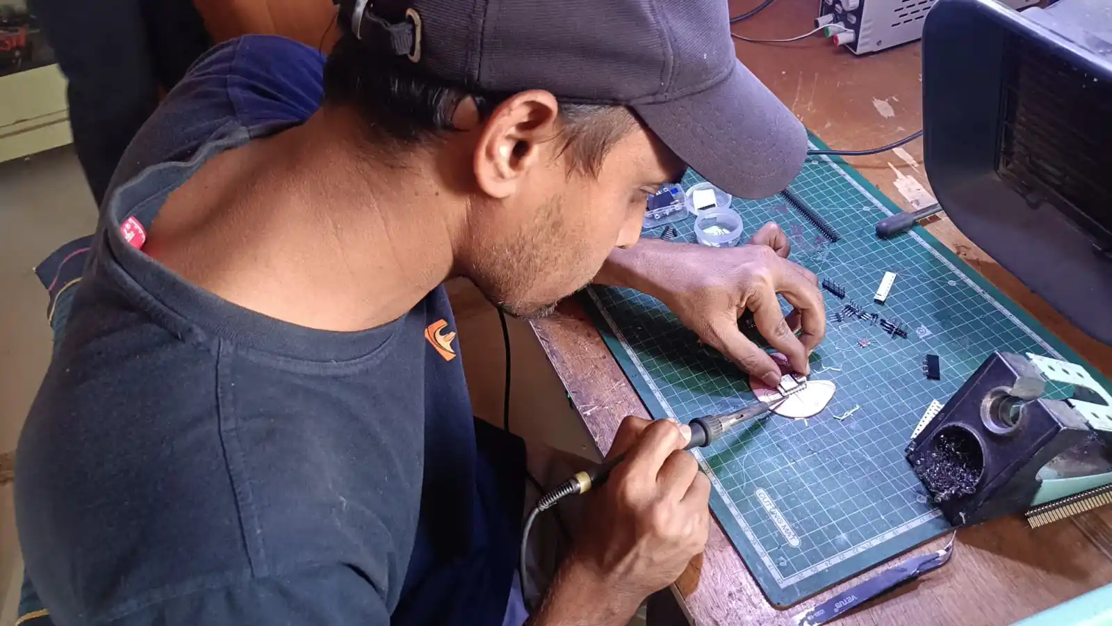
finally after soldering the commponents.
on the pcb board and tesing the pcb board using the multimeter and conneting thr power supply to chek the pcb board is working or not.
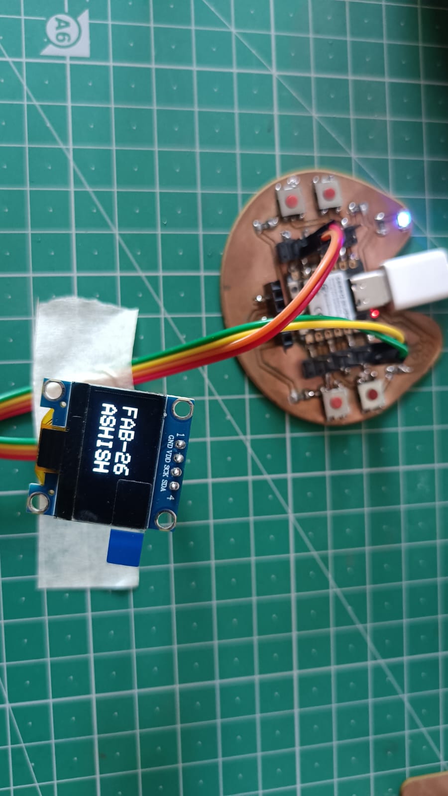
After designing the board, I tested it by connecting an OLED display. I connected the SDA, SCL, VCC, and GND pins to the board. Then, I uploaded a simple code to display the text "Fab-26" and "Ashish" on the OLED screen to verify that the board was working properly.
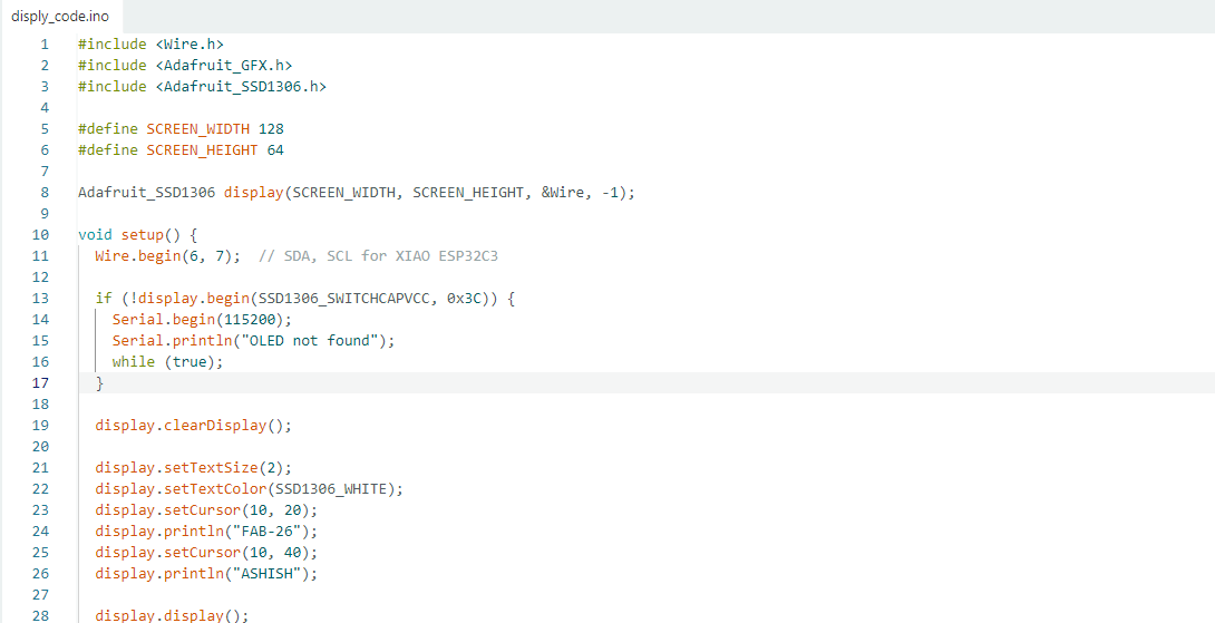
Code
Code Explanation
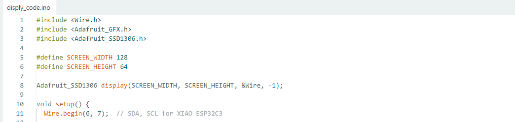
To test the OLED display, I first included the required libraries: Wire, Adafruit GFX, and Adafruit SSD1306. Then, I defined the display size as 128 × 64 pixels and created an OLED display object. In the setup function, I initialized I2C communication using GPIO 6 (SDA) and GPIO 7 (SCL) on the XIAO ESP32C3. After establishing communication, I uploaded a simple program to display the text "Fab-26" and "Ashish" on the OLED screen. This helped me verify that the OLED display and my custom board were working correctly.
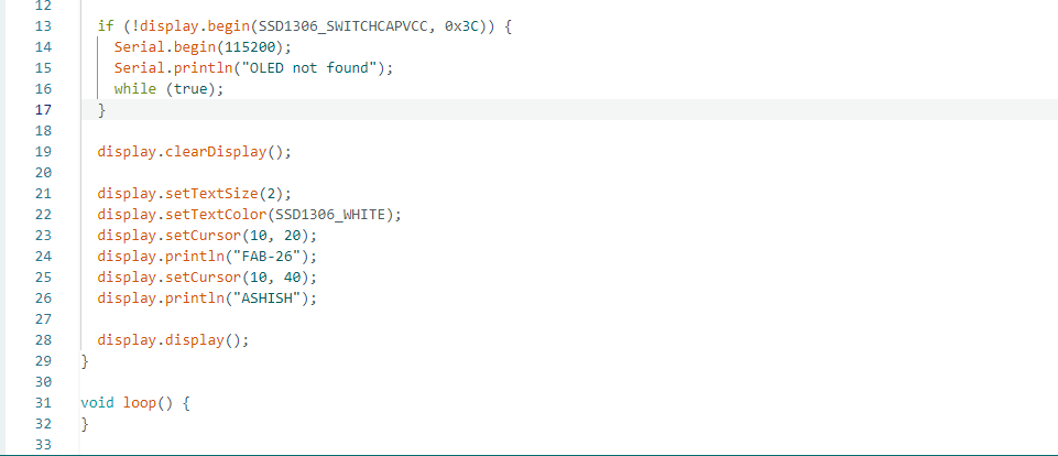
This part of the code initializes the OLED display and checks whether it is connected properly. The command display.begin(SSD1306_SWITCHCAPVCC, 0x3C) starts communication with the OLED display using the I2C address 0x3C. If the display is not detected, the program starts serial communication at 115200 baud rate and prints the message "OLED not found" in the Serial Monitor. The while(true); statement stops the program from running further until the issue is fixed.
After successful initialization, display.clearDisplay(); clears the OLED screen. The command display.setTextSize(2); sets the text size, while display.setTextColor(SSD1306_WHITE); sets the text color to white. The display.setCursor() function positions the text on the screen. The program then displays "FAB-26" at position (10, 20) and "ASHISH" at position (10, 40). Finally, display.display(); updates the OLED screen and shows the text. The loop() function is empty because the text only needs to be displayed once when the board starts.
Faced problem in this week
I am choos the wrong file for the milling process and i have to waste the pcb board and i have to again start the process from the beginning milling process. this was a learing experience for me and i learn how to avoid this type of mistake in the future and how to properly organize and manage my desigen files.
Another challenge was ensuring that the PCB board was securely fixed to the milling bed. During the milling process, I noticed some movement of the board, which caused misalignment and inaccuracies in the milling. To address this, I used additional double-sided tape to reinforce the attachment of the PCB to the milling bed, which helped to stabilize it during the milling process.
Download all files from here
source code