Introduction
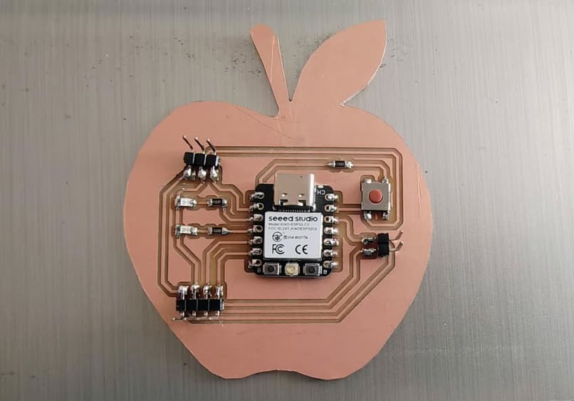
During this week, I worked on designing, fabricating, and testing my own embedded microcontroller system. I designed a custom PCB with an ESP32-C3 microcontroller, along with components like a push button, LEDs, and resistors. After completing the design, I milled the PCB using the MonoFab SRM-20 machine by generating toolpaths in the Mods software and operating the machine through VPanel. After milling, I soldered all the components on the board and checked the connections. Finally, I programmed the microcontroller and tested the system by using a push button as input and observing the LED output. This assignment helped me understand the process of building and testing an embedded electronic system.
Individual assignment
Task:This week, Task is to design and test the system. I designed and tested an embedded microcontroller system. I created the PCB design, milled the board, and assembled the electronic components on it. After assembling, I programmed the microcontroller and tested the circuit to check if all components such as the LED and button were working properly. This process helped me understand the complete workflow of designing, building, and testing an embedded system.
Group assignment
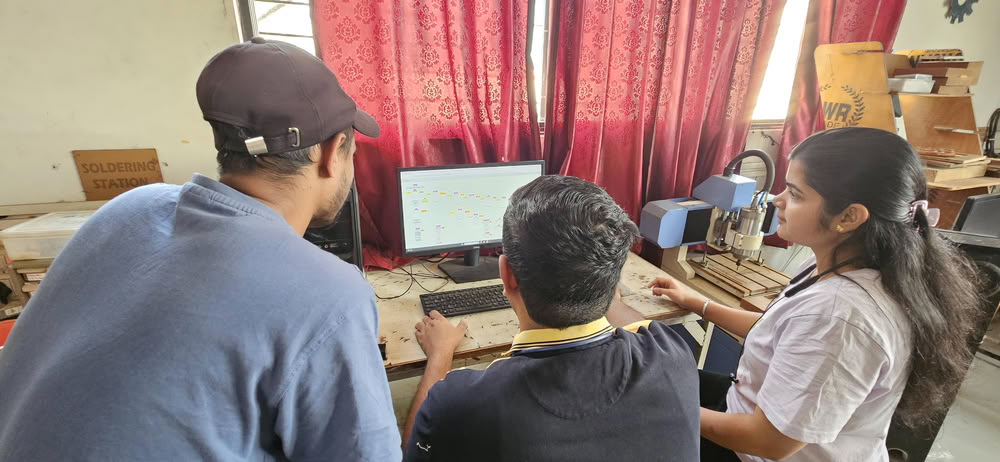
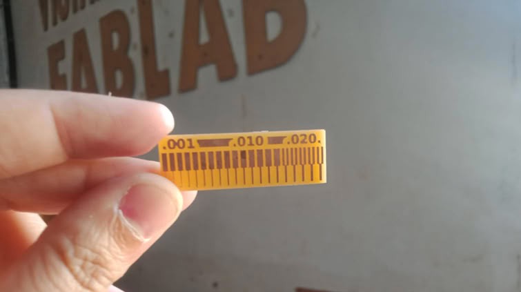
Task:During this week, we explored the electronics production process, especially PCB milling. First, we studied the design rules that need to be tested before manufacturing a PCB. For this purpose, we downloaded a test rule PNG file provided on the Fab Academy website by Neil Gershenfeld. After downloading the file, we used Mods CE to generate the milling toolpath from the PNG image. Next, we prepared the PCB milling setup by installing the required machine software, connecting the machine, and setting the correct origin position. Then the milling process was started using the generated toolpath file. After the milling was finished, we carefully observed the result to evaluate and understand the PCB design rules and milling accuracy.
Link to view group assignmentGroup Assignment
Electronic Production
Electronic production is the process of designing, manufacturing, assembling, and testing electronic circuits or devices using printed circuit boards and electronic components.
About MonoFab SRM-20
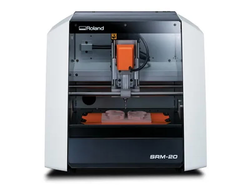
The Roland MonoFab SRM-20 is a compact desktop machine used for precise milling and prototyping of small electronic boards and parts. It is commonly used in digital fabrication labs to create PCBs directly from design files without sending them to an external manufacturer. The machine works by moving a small rotating cutting tool over a copper-clad board and removing unwanted copper to form the required circuit traces and board outline.
Because of its high accuracy, it is suitable for milling fine PCB traces and small components. The SRM-20 is easy to operate and allows users to quickly convert digital designs into physical boards, making it very useful for rapid prototyping, experimentation, and learning electronics production.
About MonoFab SRM-20 Specifications
| Specification | Details |
|---|---|
| Model | SRM-20 |
| Machine Type | Desktop 3-axis milling machine |
| Work Area (X × Y × Z) | 203.2 mm × 152.4 mm × 60.5 mm |
| Maximum Workpiece Weight | 2 kg |
| Spindle Speed | 3000 – 7000 rpm |
| Operating Speed | 4 – 1800 mm/min |
| Interface | USB |
| Power Requirement | DC 24V |
| Machine Weight | 19.6 kg |
| Supported Materials | PCB board, wax, foam, acrylic, ABS |
I used chatgpt to make this table
Equipments I used during pcb making
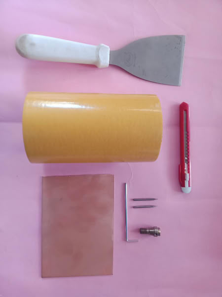
1.1/64 Inch End Mill
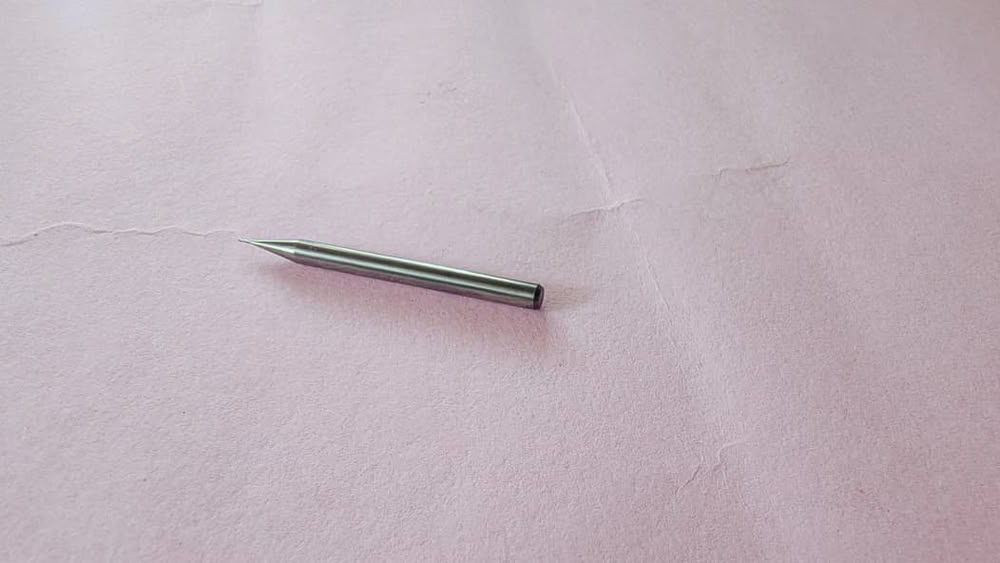
A 1/64 inch end mill is a very small cutting tool used for fine PCB milling, especially for cutting the thin copper traces on a circuit board. The diameter of a 1/64 inch tool is approximately 0.4 mm, which allows it to create precise and narrow paths between PCB traces.1/64 inch end mill is mainly used for trace cutting.
2.1/32 Inch End Mill

A 1/32 inch end mill is a cutting tool commonly used in PCB milling to cut the outline of the circuit board. The diameter of a 1/32 inch tool is about 0.8 mm, which makes it stronger and thicker than the 1/64 inch tool. Because of its larger size, it is suitable for cutting through the PCB material to separate the board from the base material.1/32 inch end mill is mainly used for cutout operations (Edge Cuts) after the traces are milled.
3.Collet

It is used in milling machines to hold and tighten the cutting tool (end mill) securely in the spindle. It acts like a clamp that grips the tool firmly so that it does not move or slip during the milling process.The collet is placed inside the spindle and the end mill (1/64 inch or 1/32 inch) is inserted into it.
4.Allen Key
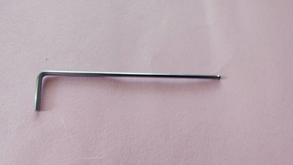
Allen key is commonly used to tighten or loosen the collet screw while changing the milling bit. For example, when inserting a 1/64 inch or 1/32 inch end mill, the Allen key helps secure the tool properly in the spindle. This ensures the cutting tool remains stable and safe during the milling process.
Kicad software Schematic Diagram
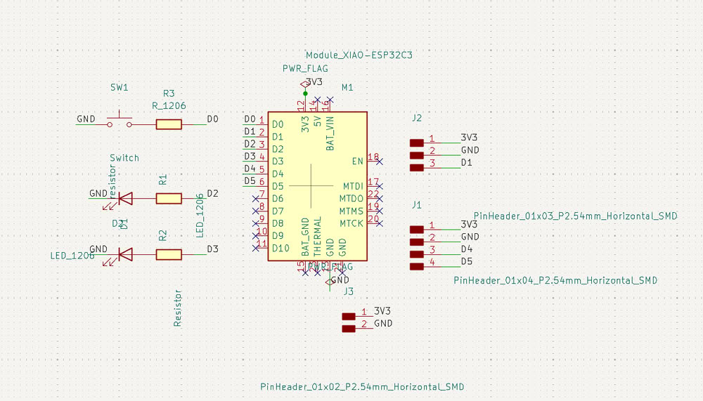
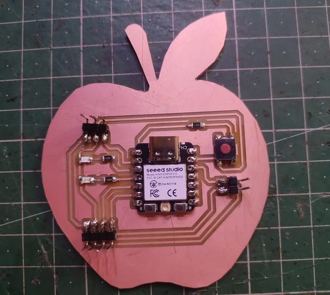
I designed the schematic for my custom development board using KiCad in electronic design assignment. The main controller used in this circuit is the Seeed Studio XIAO ESP32C3 microcontroller module. This module provides multiple GPIO pins which are used to connect input and output components.In the schematic, I added a push button switch (SW1) connected to a GPIO pin through a resistor (R3). The switch is used as an input device. Two LEDs are included as output indicators, each connected in series with a current limiting resistor (R1 and R2) to protect the LEDs from excess current.
Kicad software diagram in PCB editor
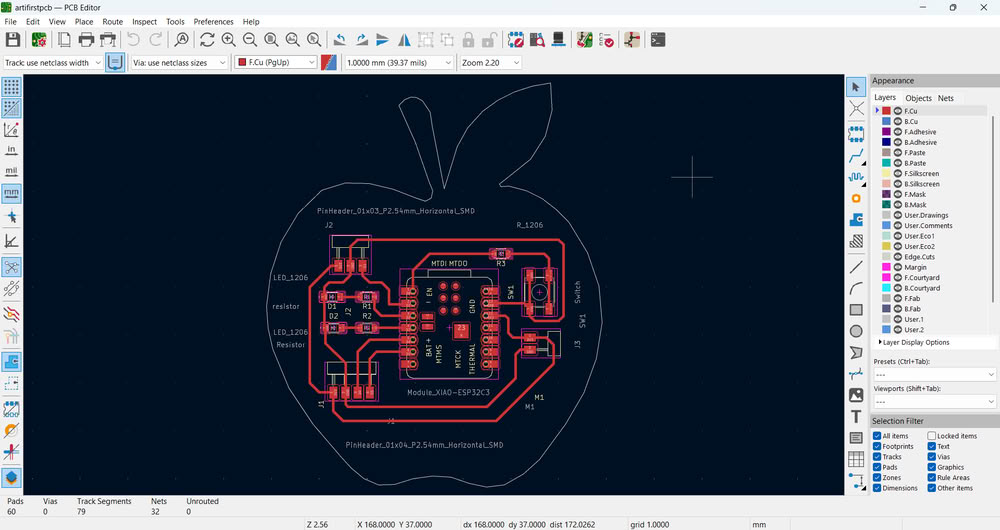
Then I go to PCB Editor where I route my PCB board.after this I plot gerber files to a specific folder for future use.
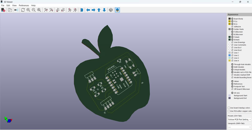
3D view of my PCB
Link to view group assignmentGroup Assignment
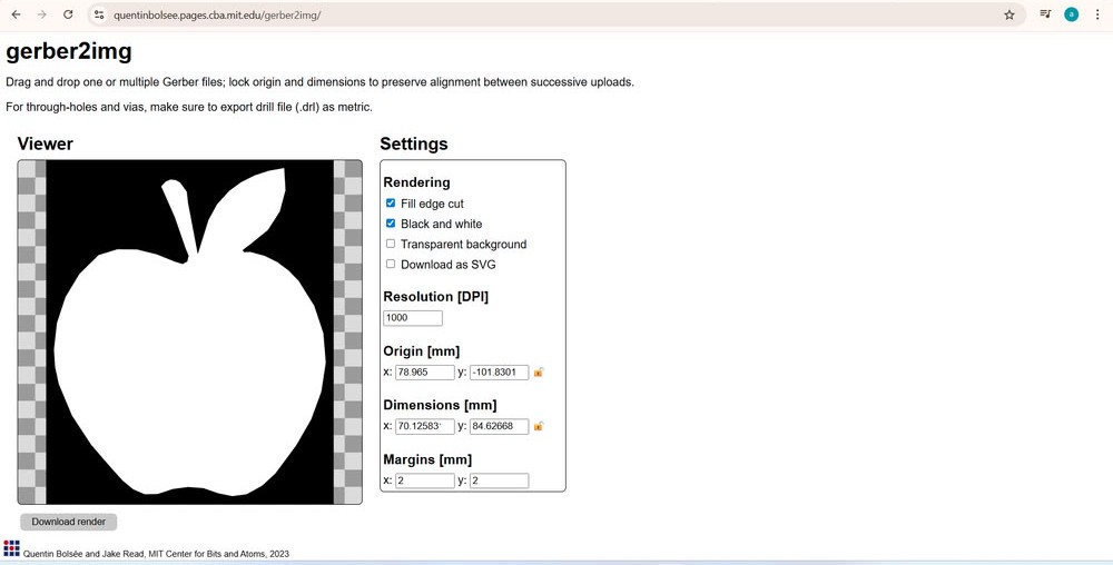
Starting with gerber to image conversion
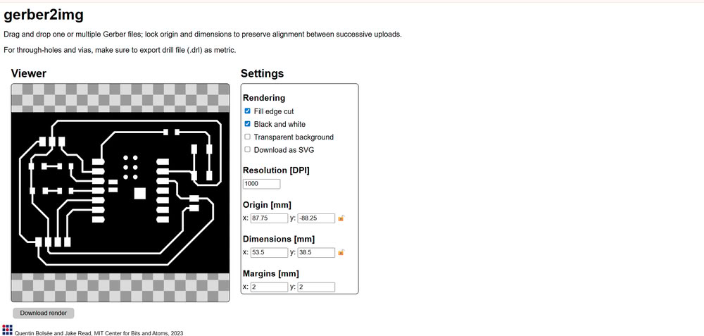
I used Gerber2Image to convert my Gerber files into PNG format. In this software, I simply drag and drop the Gerber files, and the program automatically loads and converts them into image files.
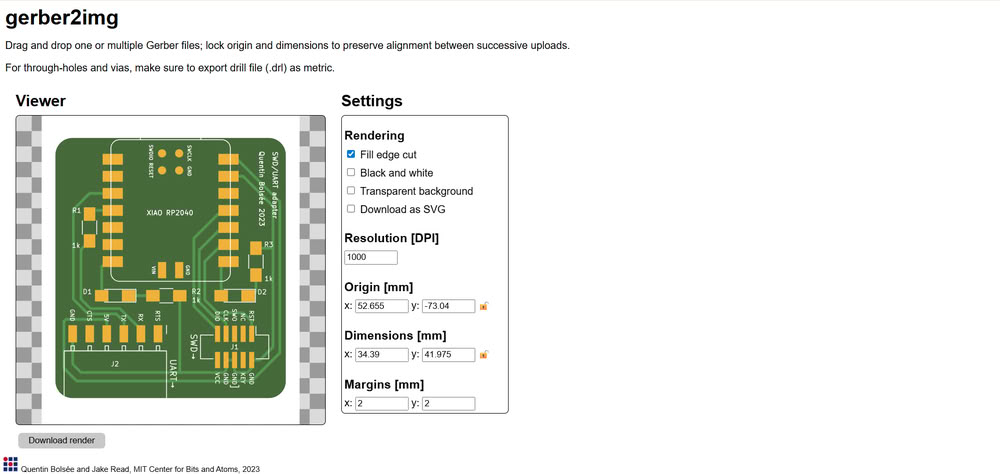
I used Gerber2Image to convert my PCB Gerber file into a PNG image. First, I selected the F.Cu (Front Copper) file and dragged and dropped it into the software. After loading the file, I chose the black and white rendering option to clearly show the PCB traces. Then, I saved the rendered output as a PNG file, which can be used for PCB milling.
After that, I selected the Edge.Cuts file, which defines the outline of the PCB board, and similarly rendered and saved it as a PNG image.
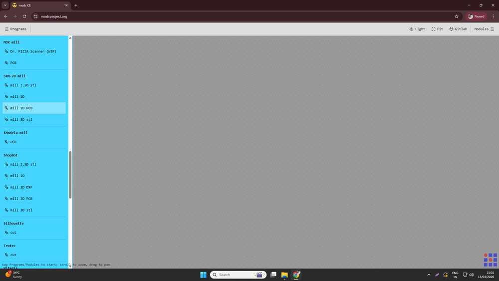
Using mods for G-code generation
I opened mods ce then click on programs and select machine I am using for pcb making.
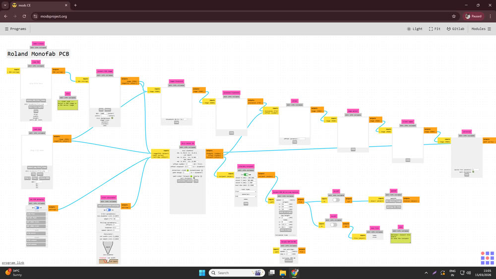
I used Mods CE to convert the PNG files into G-code for PCB milling.
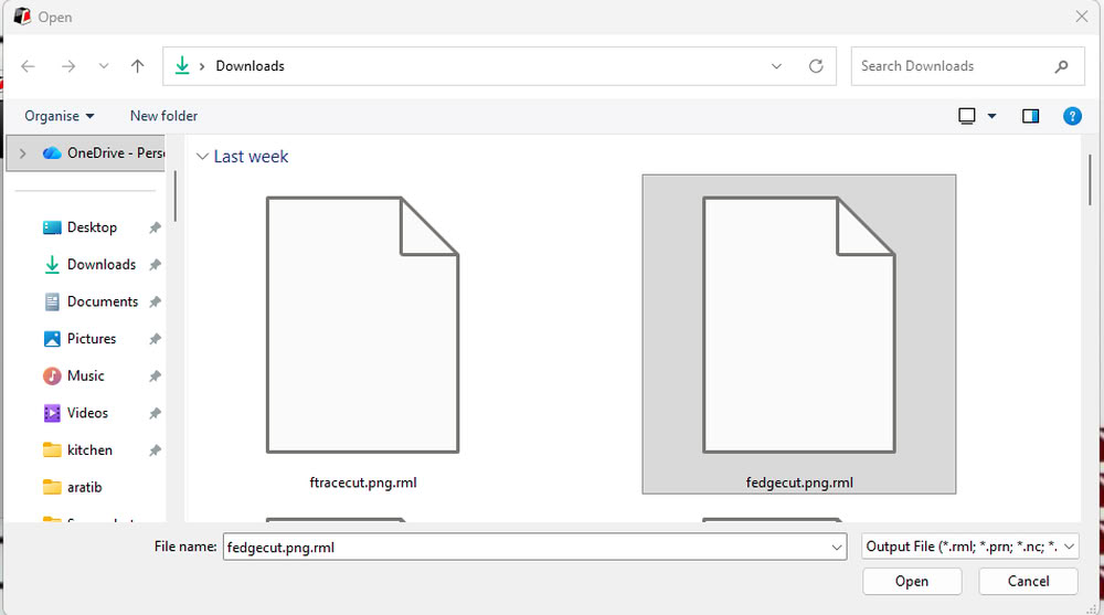
First, I opened Mods CE and clicked on Select PNG file, then I uploaded the trace cut PNG file.
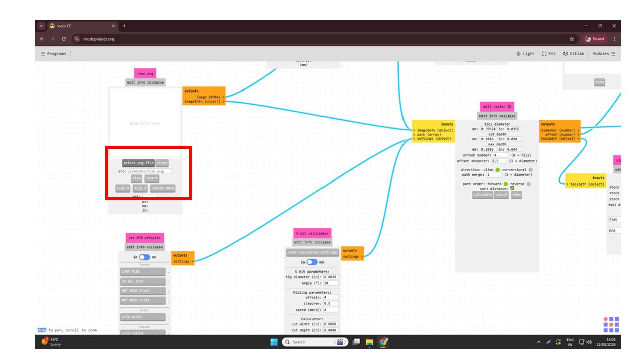
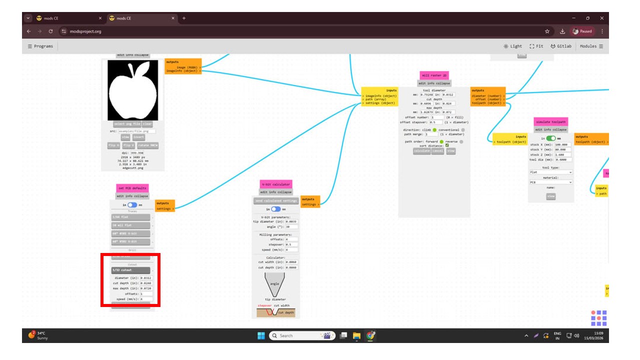
Since I was using a 1/64 milling bit for cutting the PCB traces, I selected the 1/64 tool option.
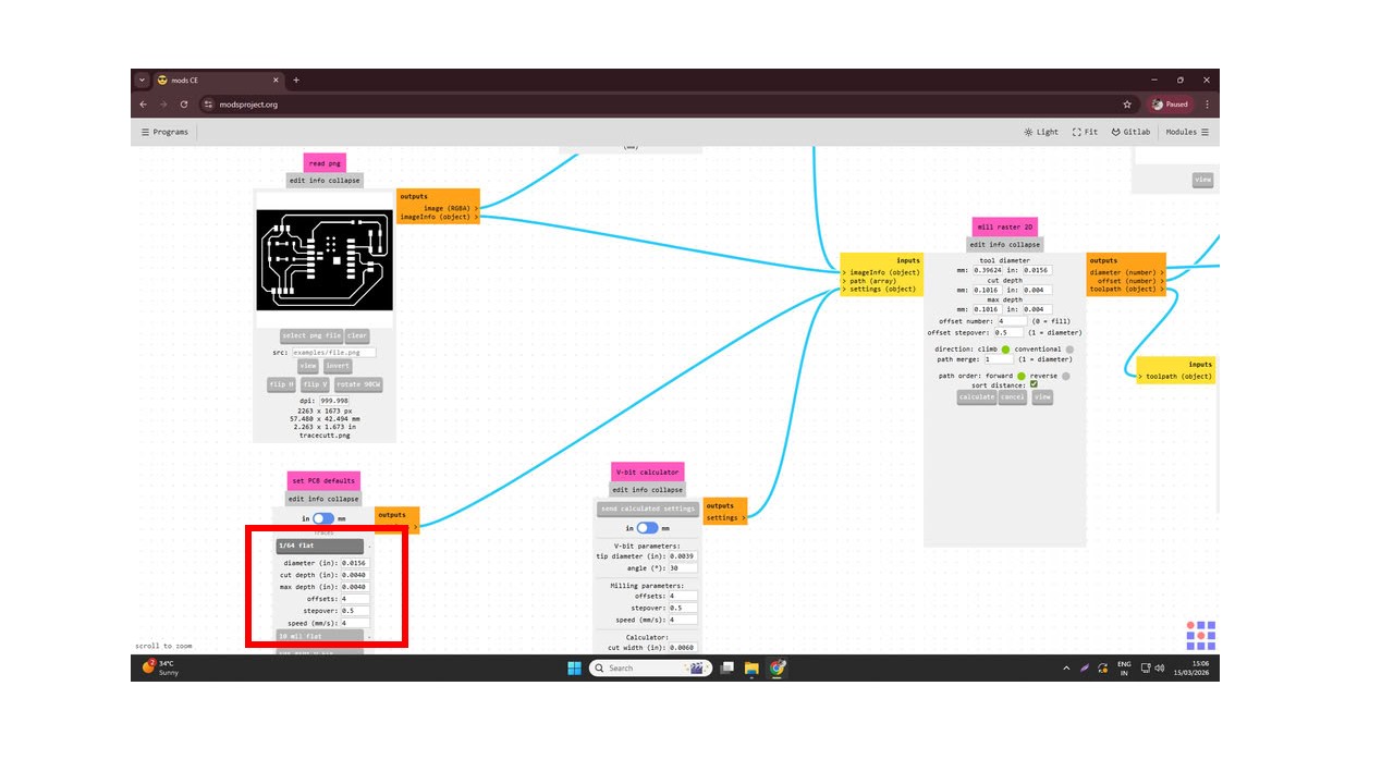
After that, I set the cutting speed to 4 mm/s and set the origin coordinates X = 0, Y = 0, Z = 0. Then I configured the settings by disabling the top button and enabling the bottom one to prepare the file for saving.
. Finally, I clicked on Calculate, and the software generated and saved the .rml file.
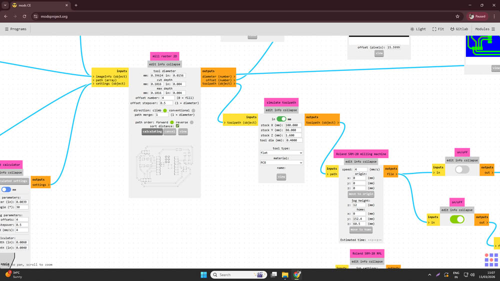
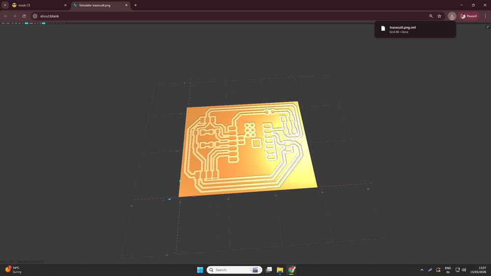
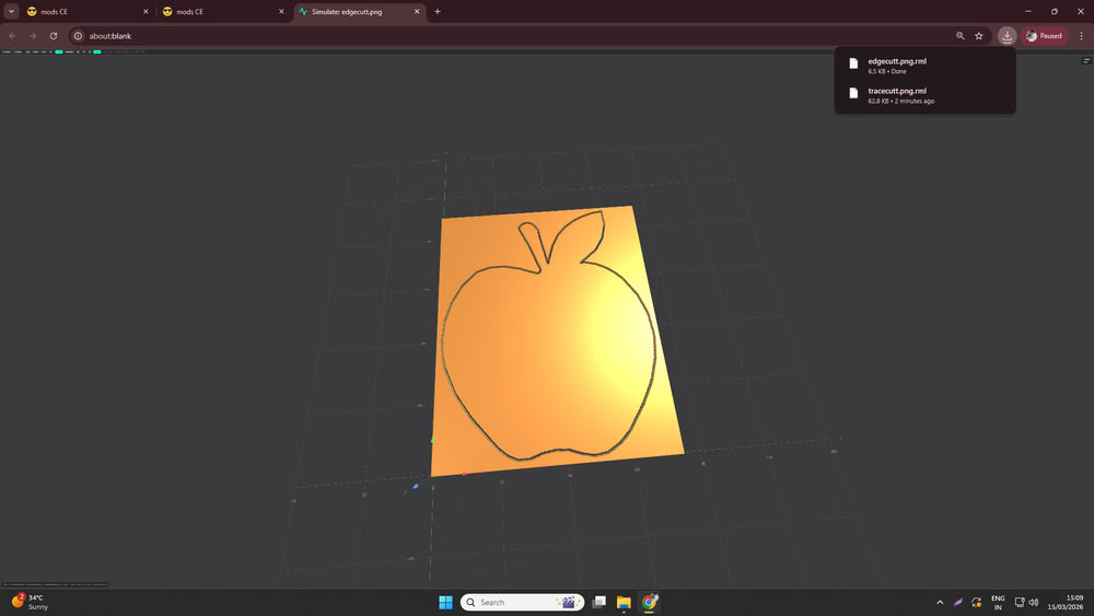
This file is then used for milling the PCB, and the generated preview shows how the PCB simulation will look after the milling process.
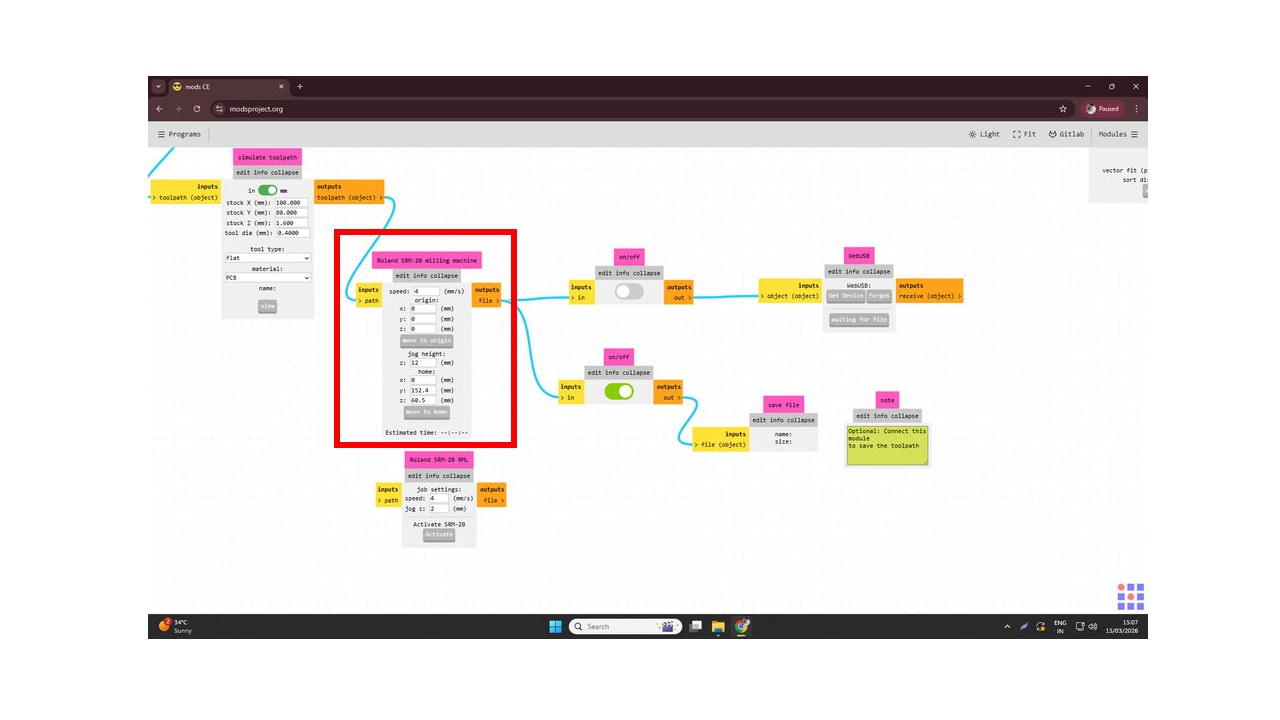
Similarly, I uploaded the Edge.Cuts PNG file into Mods CE to generate the toolpath for cutting the PCB outline. After selecting the PNG file, I chose the 1/32 cutout tool option since a 1/32 milling bit is used for cutting the board edges.
Then I set the speed to 4 mm/s and defined the origin coordinates as X = 0, Y = 0, Z = 0. After that, I configured the settings by turning off the top button and enabling the bottom one to prepare the file for saving. Finally, I clicked on Calculate, which generated the toolpath and saved the .rml file.
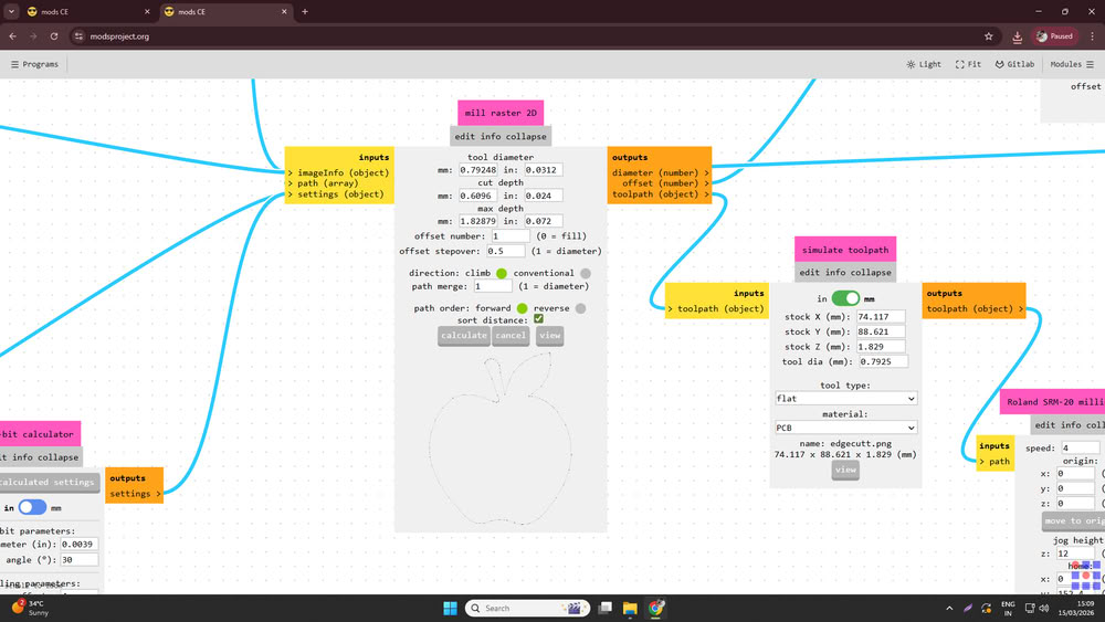
Before starting the milling process, the software displays a simulation preview, allowing us to check how the PCB outline will be cut on the machine.
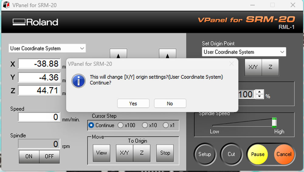
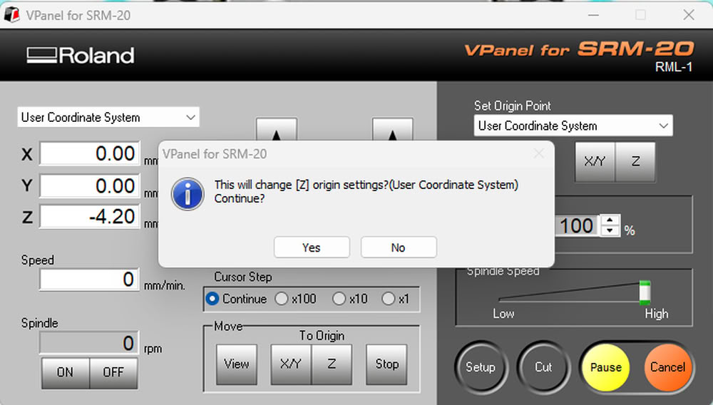
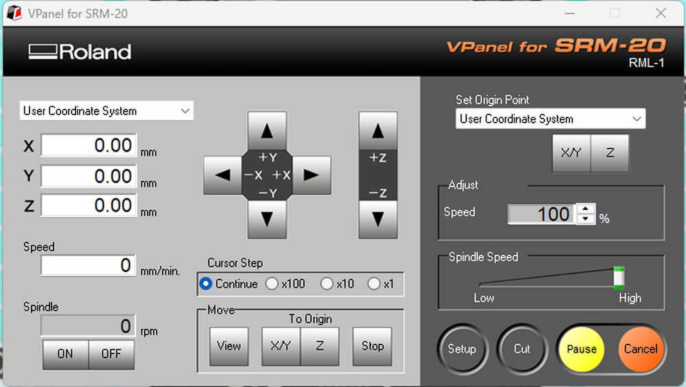
Using V-Panel for tracing and cutting process:-
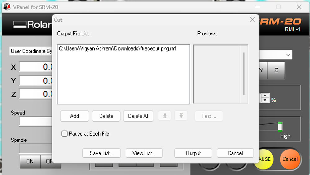
After generating the .rml files, I used VPanel software for the PCB tracing and cutting process.
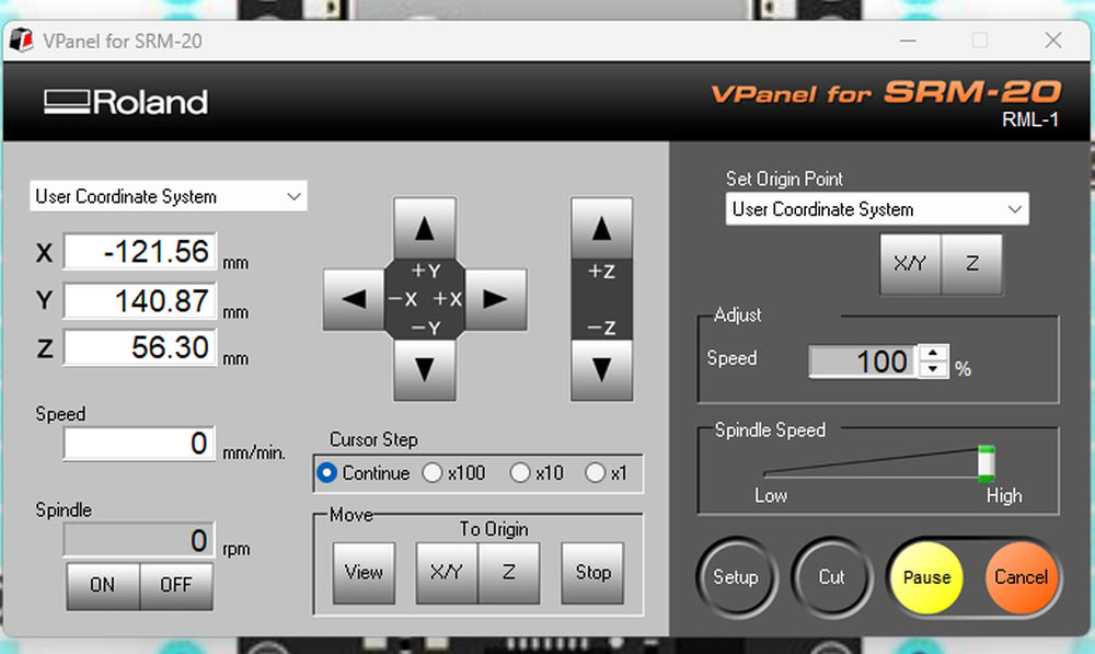
First, I installed the 1/64 inch bit for trace cutting.
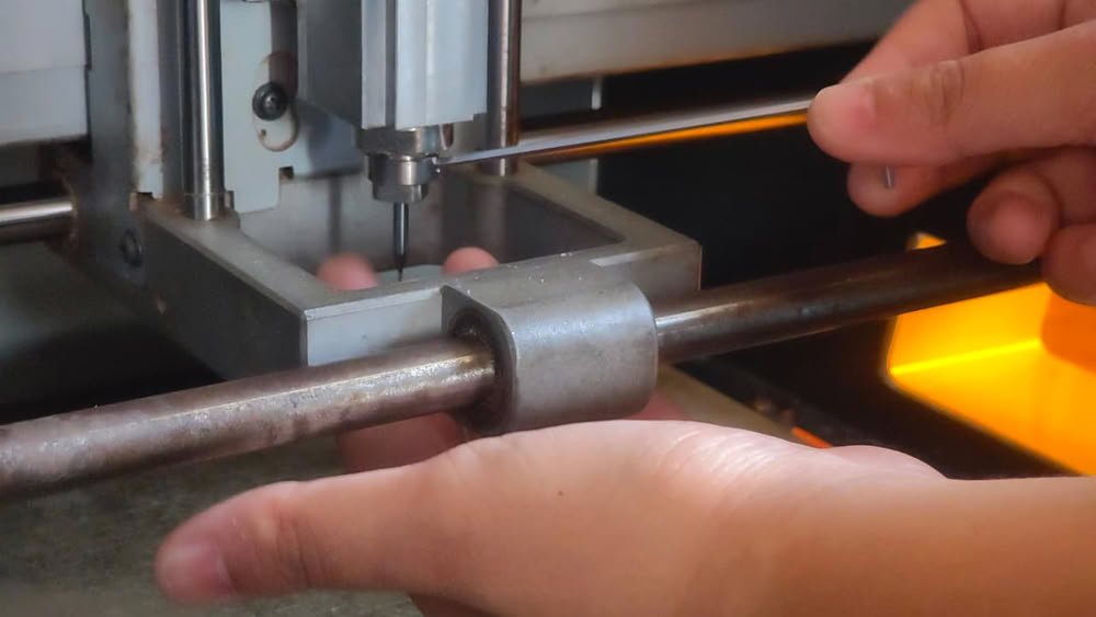
. I positioned the bit at the required location on the PCB board and set the X and Y origin points.
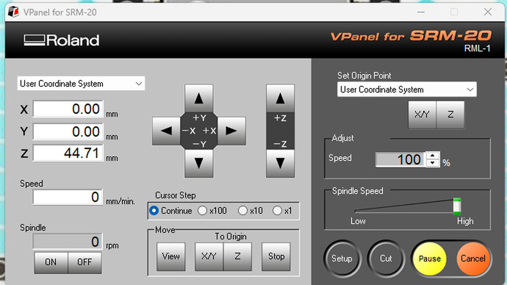
Then, I carefully lowered the bit to the surface of the board and set the Z-axis to zero.
Then I go to cut option.
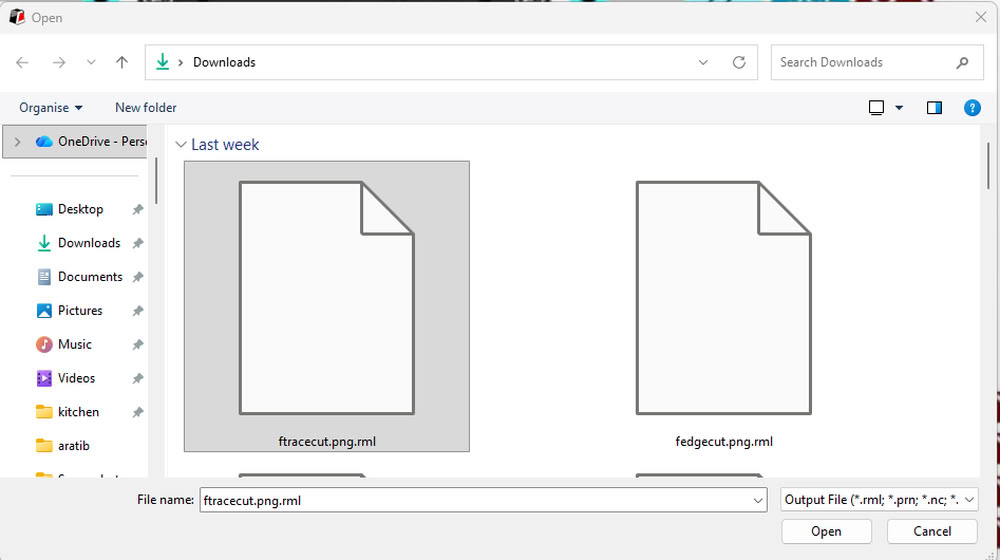
I clicked on add option.
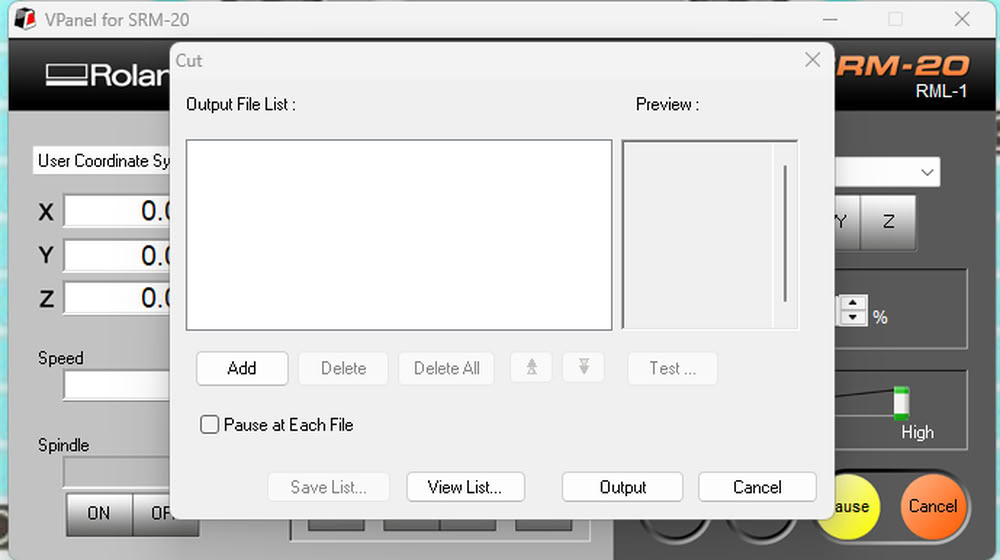
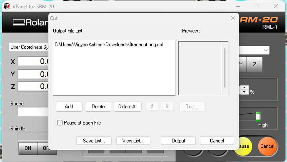
I select the trace cut file.
I clicked on output to start the machine.
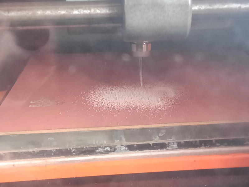
Tracecutting get started.
Once the trace cutting was completed, I replaced the 1/64 inch bit with a 1/32 inch bit for the edge cutting process.
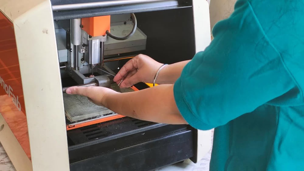
Then, I select the edgecut file
and click on output.
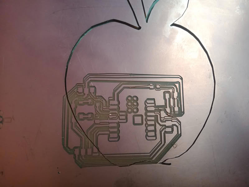
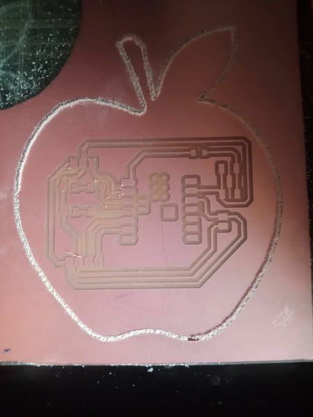
Initially, the edge cut was not aligned properly with the trace cut and traces also get damaged. To solve this issue, first I set the machine bed properly and placed copper clad on the bed properly and during the Gerber2Image generation process, I set the origin and dimensions of the edge cut image to the trace cut image dimensions and origin. This ensured that the origin points matched correctly, and after making this change, the PCB was cut properly.
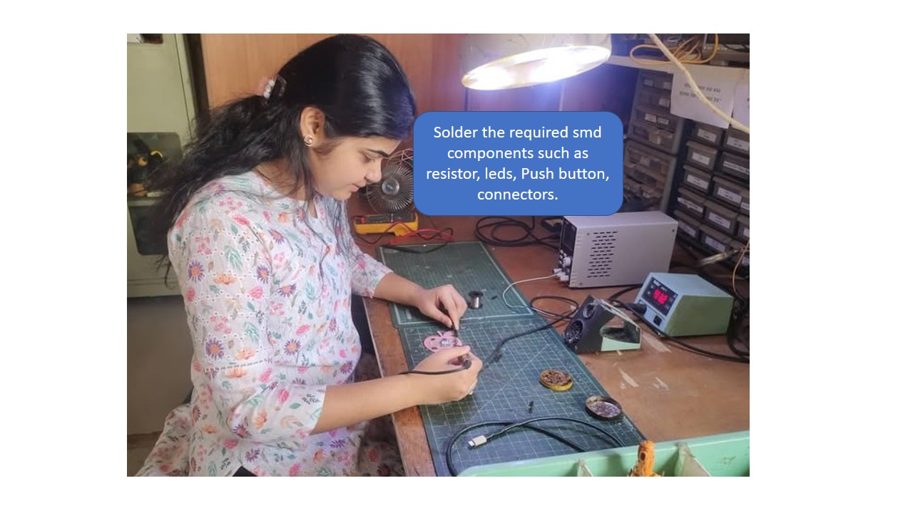
Soldering Process:-
Tools required during soldering process:-
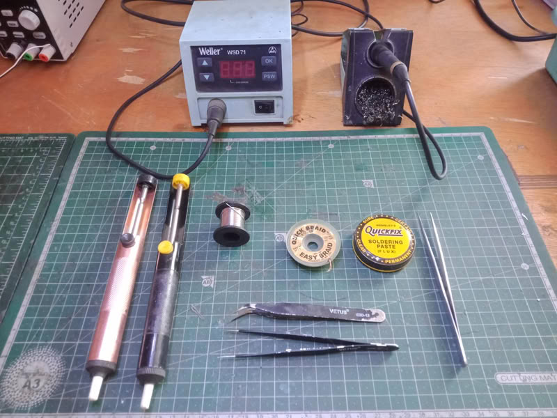
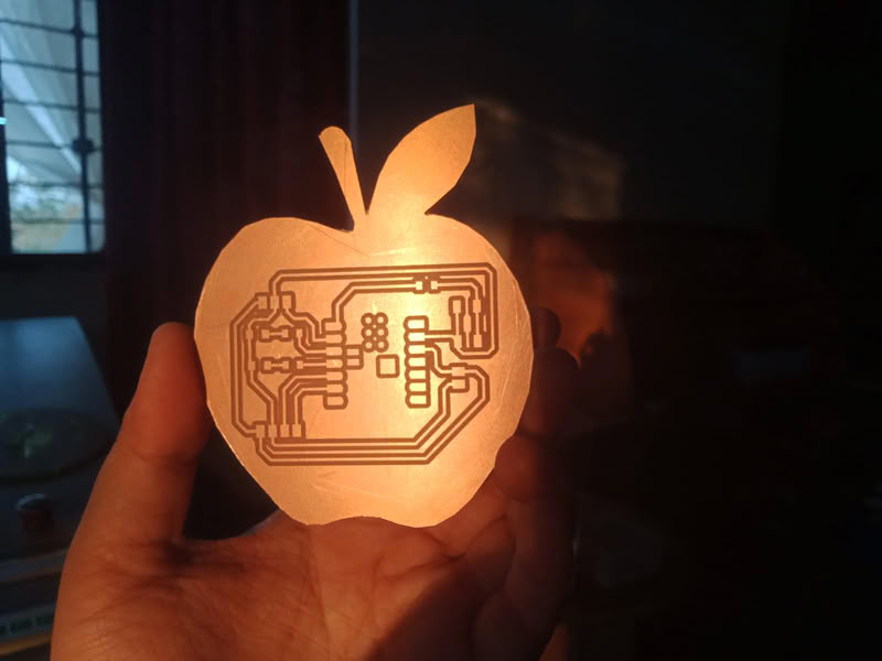
The soldering process is used to attach electronic components to the PCB after the board is milled. First, the milled PCB is cleaned properly to remove dust or copper particles. Then all the required components such as resistors, LEDs, microcontroller, and connectors are placed on their respective pads according to the schematic design. A soldering iron is heated and solder wire is applied to the joint where the component lead and copper pad meet. The heat melts the solder, allowing it to flow around the component lead and pad, creating a strong electrical and mechanical connection. This process is repeated for all components on the board. After soldering, the board is visually inspected to ensure there are no loose connections, excess solder, or short circuits between the pads.
 |
 |
Uploading code:-
I used Arduino IDE to upload the program to my PCB. First, I connected my board to the computer using a USB cable and opened the Arduino IDE. Then I selected the correct board and port from the tools menu. After that, I wrote the code to make the LEDs blink one by one and clicked on the Upload button to transfer the code to the microcontroller on my PCB. Once the code was successfully uploaded, the LEDs on the board started blinking sequentially. The following video shows the complete process of uploading the code and the LEDs blinking one by one on the board.
Code and .rml design files
Click here to download original files