Week 6: Electronics Design
Overview
This week's assignment required using an EDA tool to design a development board that uses parts from the lab’s inventory to interact and communicate with an embedded microcontroller. My work this week is directly connected to my final project: a wearable and handheld console system that guides users through design iterations based in entrepreneurship and innovation using informed journaling prompts. For this week I focused on learning Ki-CAD to design a board that will interact and communicate with a Seeed studio RP 2040 microcontroller.
Group Assignment
Group assignment: Use the test equipment in your lab to observe the operation of a microcontroller circuit board (as a minimum, you should demonstrate the use of a logic analyzer) Document your work on the group work page and reflect what you learned on your individual pageIndividual Assignment
Use an EDA tool to design a development board that uses parts from the inventory to interact and communicate with an embedded microcontrollerResearch
I am currently completing Fabricademy and will continue interating during Fabacademy. My final project in Fabricademy focuses on increasing engagement and understanding of how Labs in university settings can utilize tools, machines, and softwares to create. My final project will require the understanding of coding, 2d and 3d design, 3d print manufacturing, molding and casting, bio engineering, mechatronics, soft robotics, and textile sustainability.
Update: I scrapped my initial Final project April 2026 for a variety of resons. From here I will discuss what was mentioned in this page's overview.
What is Interface and Application Programming?
Electronics design is the bridge between a theoretical idea and a physical, functional device. It is the process of defining how electricity will flow through various components. Components are pieces of the internal machine like microcontrollers, resistors, and LEDs. These pieces perform specific tasks based on the machine being utilized. This week, I am moving beyond just connecting parts utilizing a breadboard (breadboards aren’t a very permanent or reliable way to connect components to one another). I will be learning to build a permanent system by creating a custom Printed Circuit Board (PCB). This involves two main stages: schematic capture, where I will define the logical connections between parts, and PCB Layout, where I will physically route those connections onto copper traces that can be fabricated in the lab.
Software Comparison
- Kicad Vs Autodesk Fusuon360Design
- Autodesk Fusion: While powerful and widely used in professional settings, it is a proprietary tool that can sometimes feel overly complex due to its integration with 3D CAD features. The licensing can also be a hurdle for open-source projects, as it is pretty expensive (in my opinion).
- KiCad: I was attracted to KiCad mainly because it is a completely free, open-source software. It offers separate editors for schematics and PCB layout, which helps me focus on one task at a time. I was also attracted to its Electrical Rules Check (ERC) and Design Rule Check (DRC) because they can catch errors before I waste material I don't have on a bad etch, cut, or mill.
- I’d also like to mention that I am trying to expand my personal design skills as much as possible and have already explored Fusion a bit, so I see this as a great opportunity to explore new software.
Before starting my design, I explored different Electronic Design Automation (EDA) tools to see which fit my workflow best.
Group Assignment - Remote Student, no group page to link to
Before committing to my schematic design, I wanted to physically verify that my XIAO RP2040 was behaving the way I expected it to on paper. I used a multimeter to run two basic checks: voltage and continuity.
For voltage, I set my multimeter to DC voltage mode and placed the red probe on the 3V3 pin of the XIAO and the black probe on GND. The board was powered via USB-C. The multimeter read approximately 3.3V, which confirmed that the onboard voltage regulator was outputting a stable reference. I believe this is exactly what my pull-down resistor circuit depends on to hold GPIO pins at a clean LOW state when buttons aren't pressed
I then tested continuity to verify that my GND connections were actually connected to each other across the board. I touched both probes to different GND points and listened for the multimeter's beep. The beep confirmed that my ground net was correct and that my circuit wouldn't have floating or disconnected ground paths that could cause issues later.
These two checks gave me confidence that the physical board matched my schematic intent before I moved into layout and fabrication planning.
My Goals This Week
- The Brain: I am using an embedded microcontroller (XIAO RP2040) that I ordered from Amazon as our lab’s inventory did not have any microcontrollers on hand.
- Interaction: I’m including local Input/Output (I/O) components that align with my final project so I can physically interact with the code.
- Communication: I am ensuring the board has a USB-c connection (via my XIAO) to communicate with my computer, which is vital for programming and debugging via the Serial Monitor.
- Fabrication Readiness: I really want to attempt a “hacker” version PCB and use acrylic and copper tape cut on the lab’s vinyl cutter (utilizing Inkscape). I’ve also researched our lab's copper board milling capabilities (specifically the 1/64" and 1/32" endmills) to ensure my trace widths and clearances are set correctly in my EDA tool's design rules.
For this assignment, my goal is to design a development board from scratch rather than modifying an existing project. My concept involves:
My Takeaways from the Group Assignment
- I found that the python machine module made it straightforward to read GPIO pin states directly, which helped me understand how the microcontroller interprets the HIGH and LOW signals I designed into my pull-down resistor circuit.
Connection to Final Project
My final project is a dual-device system: a handheld console and a wearable that work together to guide users through entrepreneurial and innovation-focused design journaling. The system uses prompts to encourage the user to examine assumptions, reframe problems, and build new cognitive habits through reflective writing.
This week's work builds the electrical design layer of that system:
| This Week | Final Project |
| Computer runs the journal app | Handheld console runs the app |
| USB serial communicates with PCB | Console communicates with wearable wirelessly (BLE) |
| Button on PCB advances prompts | Physical buttons on console advance prompts |
| Entries saved to local .json file | Entries saved to SD card on console |
| LED confirms save action | NeoPixels + vibration confirm actions on wearable |
| Computer screen shows UI | Console touchscreen shows UI |
Hardware | Components Used
| Component | Quantity | Purpose |
| Xiao RP2040 | REMOVED FROM PROJECT (see 'why these components' section) | Microcontroller |
| Tactile push button | 3 | Input (back, save, next SMD buttons) |
| LED | 1 | Output (confirms save action) |
| resistors | 4 | Current limiting (1 1kohm protects the LED, 3 10kohm resistors to ensure buttons have a clean LOW state) |
| 12c Header (4-pin male header) | 1 | Connection for future screens |
| Xiao RP2350 Replaces the Xiao RP2040 | May 2026 (see 'why these components section) | 1 | Microcontroller |
Why These Components
The component choices are intentionally minimal for this week's prototype. The buttons were chosen as the input because it maps directly to the final product interaction. The LED was chosen as the output because it provides immediate, unambiguous confirmation feedback, which is a core UX principle for the journaling flow: the user needs to know their entry was saved before moving on
The resistors limit current through the LED to a safe level. Without it, the LED would draw too much current from the Xiao's GPIO pin and could damage the board over time.
I prioritized adding the 4-pin pin-management to ensure the XIAO RP2040 could handle both my current UI and future expansion. I dedicated D4 and D5 specifically for an I2C communication bus via a 4-pin header, which will eventually drive an LCD. My three navigation buttons (Back, Save, and Next) are mapped to D0-D2 with 10kΩ pull-down resistors to ensure signal stability, while D3 handles the status LED. This layout leaves several pins free for the other sensors I plan to add later.
I was advised during a saturday open global session to consider using a power bank to safely power my device and will be utilizing a USB-C power bank to do so safely in my final project. Since the XIAO RP2040 features an integrated USB-C port with a voltage regulator, I will power the device directly via a portable power bank. This allows me to use the same port for both firmware updates on my Windows PC and standalone operation in the field. Also, because of this use case, I made sure the XIAO is placed at the very edge of my PCB design so that the USB-C cable's plastic housing doesn't hit the board when I try to plug it in!
UPDATE: During the Systems Integration weekly review I learned that the RP2040 was not the best choice due to energy considerations and chose to switch to the Xiao RP 2350. For more info on those energy considerations, see this link:
PCB Design | KiCad Schematic
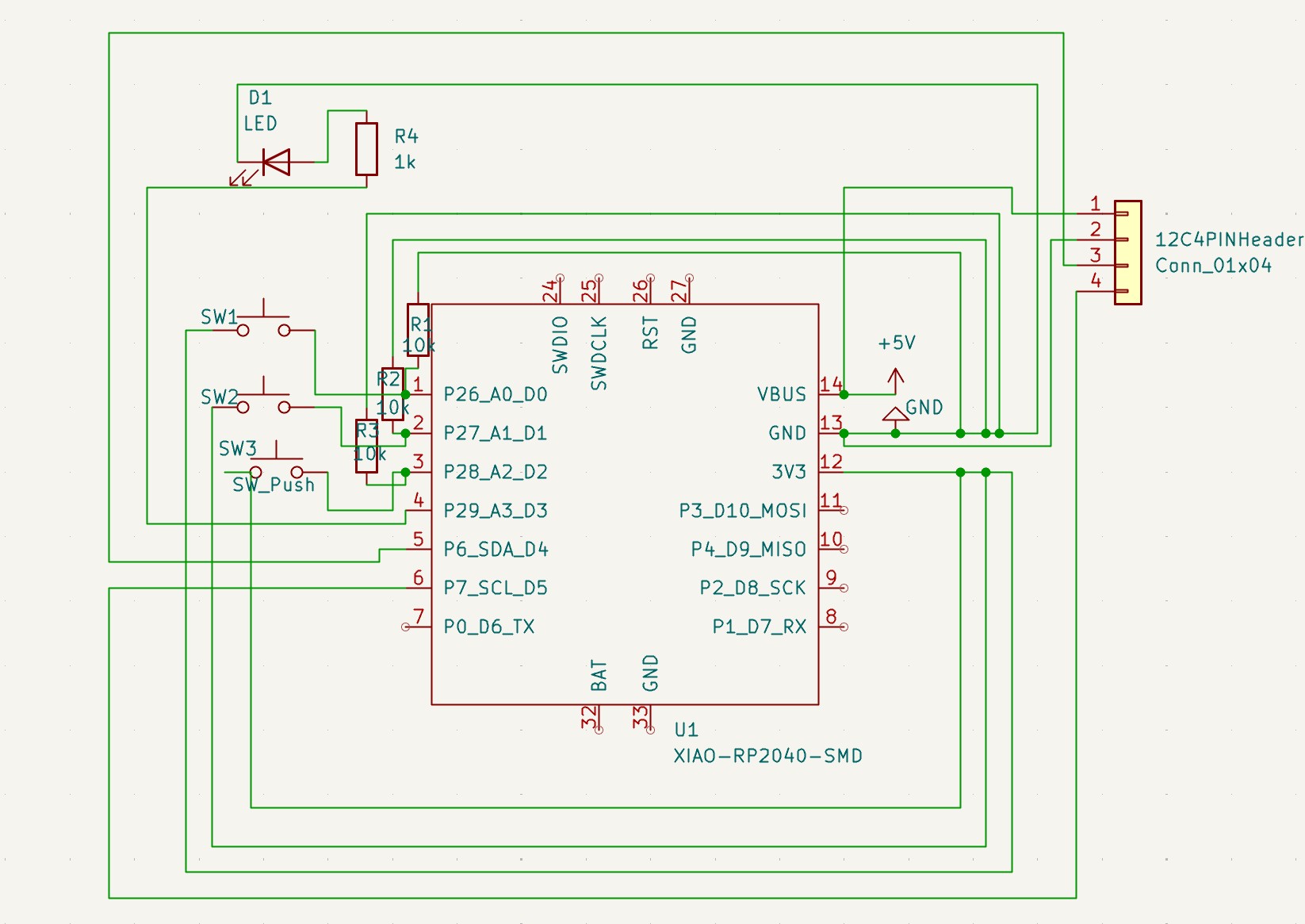
KiCad Schematic RP2040 Version
Design Decisions
My PCB design for this week implements the minimum viable circuit to satisfy the Fab Academy requirement: one input device (button) and one output device (LED), connected to a microcontroller (Xiao RP2040).
The schematic was drawn in KiCad [Version 10.0].
Schematic Walkthrough
-
The circuit consists of Seven main components:
- U1 — Xiao RP2040 The microcontroller. It receives power via USB-C and communicates with the computer over USB serial. Pin D0 is configured as a digital input (with internal pull-up) for the button. Pin D1 is configured as a digital output for the LED.
- SW1 (SW2/SW3) — Tactile push buttons One leg connects to pin D0 on the Xiao. The other leg connects to GND. When pressed, D0 (D1/D2) is pulled LOW, which the firmware detects as a button press event. The internal pull-up resistor on the Xiao keeps the pin HIGH when the button is not pressed, preventing false triggers.
- R1 (R2/R3) — 100KΩ resistors In series with the tactile push buttons.
- R4 - 1KΩ resistor In series with the LED. Limits current to a safe level for the Xiao's GPIO pin (max 12mA per pin on the RP2040). With a 3.3V output and a ~2V LED forward voltage, the current through the circuit is approximately (3.3 - 2.0) / 100 = 13mA — within safe limits.
- LED1 — LED Anode connects to the resistor (which connects to D1). Cathode connects to GND. Lights up when D1 is pulled HIGH by the firmware, confirming a save action to the user.
- J1 — USB-C (onboard) The Xiao's built-in USB-C connector serves as both power supply and serial communication interface. This is noted on the schematic as the data/power interface
- 12C 4-Pin Male Header
UPDATE: Note that since this schematic design, I've updated my plans for my final project to use the XIAO RP-2350 as my microcontroller. See the 'why these comonents' section above for more info.
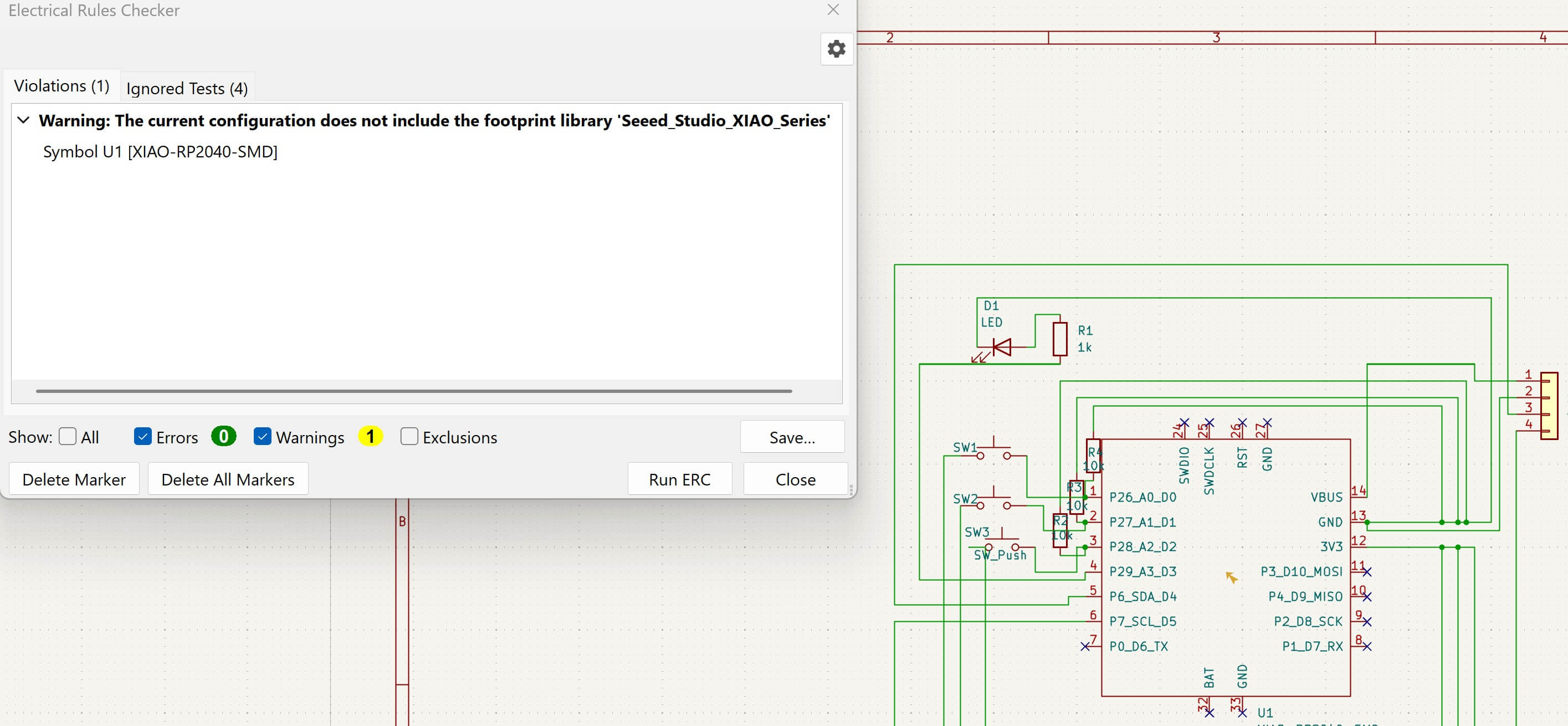
ERC (Electric Rules Check) of my Schematic
I'm receiving a warning becuase the Seeed library isn't installed in this KiCad instance.
Problems Encountered
- What I tried: In my KiCad workflow, I began by importing the Seeed Studio GitHub library to ensure my component footprints matched the XIAO RP2040's unique pin spacing.
- Result: I was able to correctly assign components to my schematic
- What I tried: To future-proof the design for an LCD or other screen, I broke out the I2C bus on D4 and D5 to a dedicated 4-pin header, powered by the 5V rail provided by the USB-C power bank input.
- Result: I was able to correctly leave room for further iteration within my board.
- What I tried:I rewired each button circuit so that it follows the correct pull-up resistor pattern:
- One leg of the resistor connects to 3V3
- The other leg of the resistor connects to the GPIO pin (D0 for SW1, D1 for SW2, D2 for SW3) and to one leg of the button at the same junction point
- The other leg of the button connects to GND
- Result: With the corrected wiring, each GPIO pin now has a stable default voltage. When a button is not pressed, current trickles from 3V3 through the 10kΩ resistor to the pin, holding it at HIGH. When a button is pressed, it creates a direct path to GND, which overrides the resistor and pulls the pin to LOW. In my CircuitPython firmware, I can read this reliably. The microcontroller will now correctly detect exactly when each button is pressed and released, with no floating or phantom inputs. Each button maps to a specific action — SW1 goes back one prompt, SW2 saves the current entry, SW3 advances to the next prompt — and the console will only respond to those actions when the user deliberately presses the physical button.
- What I tried: In my KiCad workflow, 3V3 → Switch → Pin one side of resistor, other side of resistor → GND. I'm hoping my pull-down configuration is sound. When the button is open, the pin is held LOW through the resistor to GND. When pressed, 3V3 is connected directly to the pin (pulling it HIGH). I will make sure my code is equipped with digitalRead() expecting HIGH on press. I'm also making sure to use INPUT mode (not INPUT_PULLUP) in my code, since I have external pull-downs.
- Result: I was able to correctly assign my netlist
Results
Reflection
Connection to Final Project
This week's work is the first functional prototype of my final project's application layer. The journal app built this week will evolve through the following stages toward the final product:
- Next step (Electronics Production): Add a second Xiao-based PCB as the wearable component, with a vibration motor and NeoPixels as actuators. The console PCB will also gain an LED display to show the current prompt number, and an SD card module to store entries locally without a computer.
- Prototype phase:Replace the computer application with firmware running directly on the handheld console. The console's touchscreen will handle text input, and entries will write to the SD card rather than a JSON file on the computer.
- Final product:The computer is removed from the system entirely. The console is standalone. The wearable communicates with the console over BLE, receiving trigger signals that activate vibration and light patterns timed to the user's journaling session which provides somatic pattern interruption designed to break cognitive habit loops and encourage new thought patterns.
The design built this week remains the core of the experience at every stage. What changes is the hardware it runs on and components that enhance the UI.
Files
| File | Description | KiCad Schematic | KiCad Schematic |