

CNC Milling Machine & Tools
🏭 Roland Modela Pro II MDX-540
At Fab Lab Ulima we use the Roland Modela Pro II MDX-540, a precision CNC milling machine used for rapid prototyping through subtractive manufacturing processes. Subtractive manufacturing works by removing material from a solid surface using cutting tools, following paths generated by digital fabrication software.

The machine allows us to:
Precision engraving of PCB circuit traces on copper-clad boards.
Create molds and 3D structures for casting and prototyping.
Perform high precision cutting operations for board outlines and complex geometries.
🔧 Milling Tools
Different milling tools are used depending on the type of operation during the PCB fabrication process.
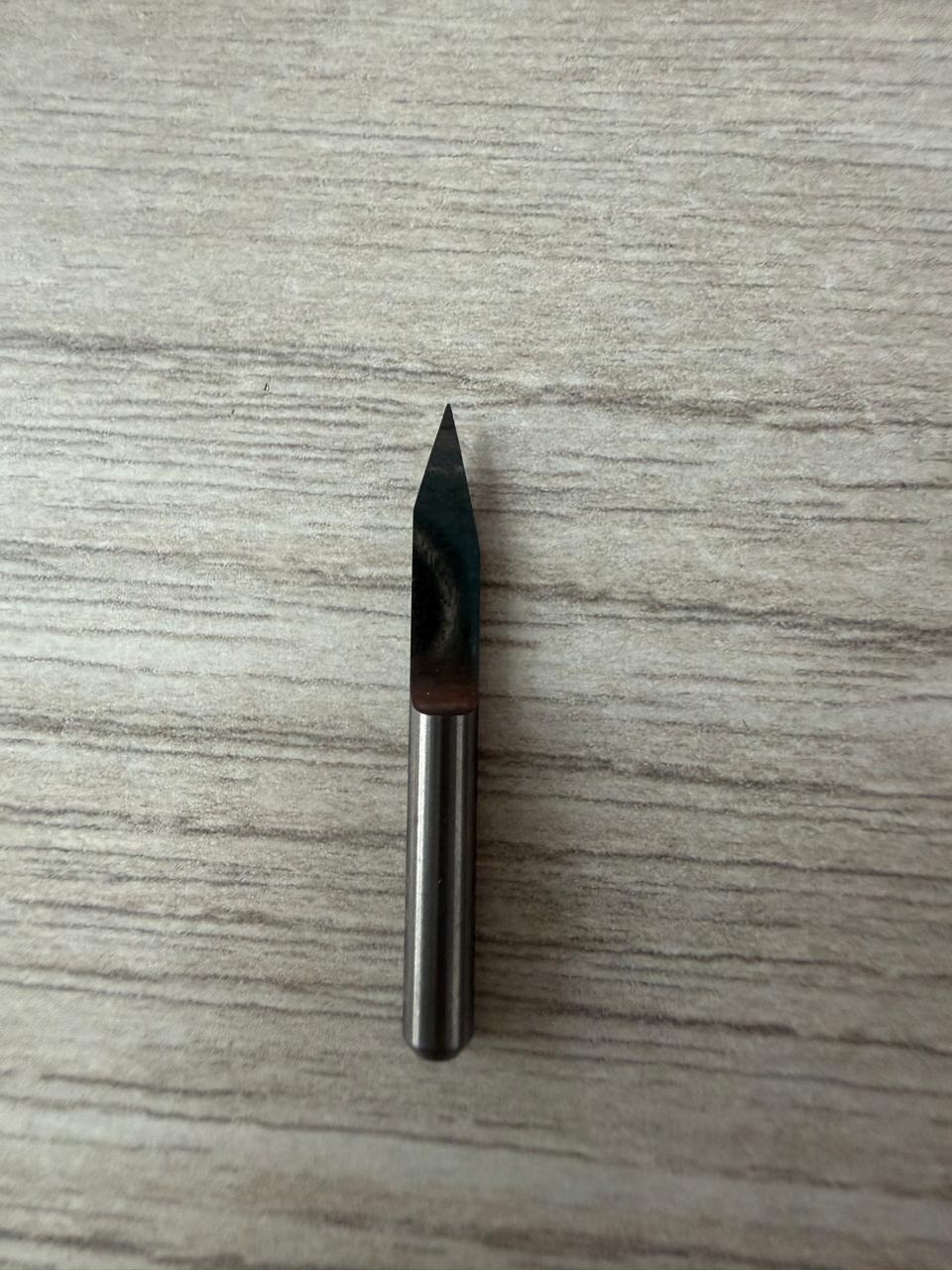
Mainly used to engrave the copper traces of the circuit. It has a V-shaped tip with an angle that commonly varies between 30° and 40°.
The cutting width depends on the depth of the tool in the Z axis — the deeper the tool penetrates, the wider the engraved trace. Correct Z calibration is critical.
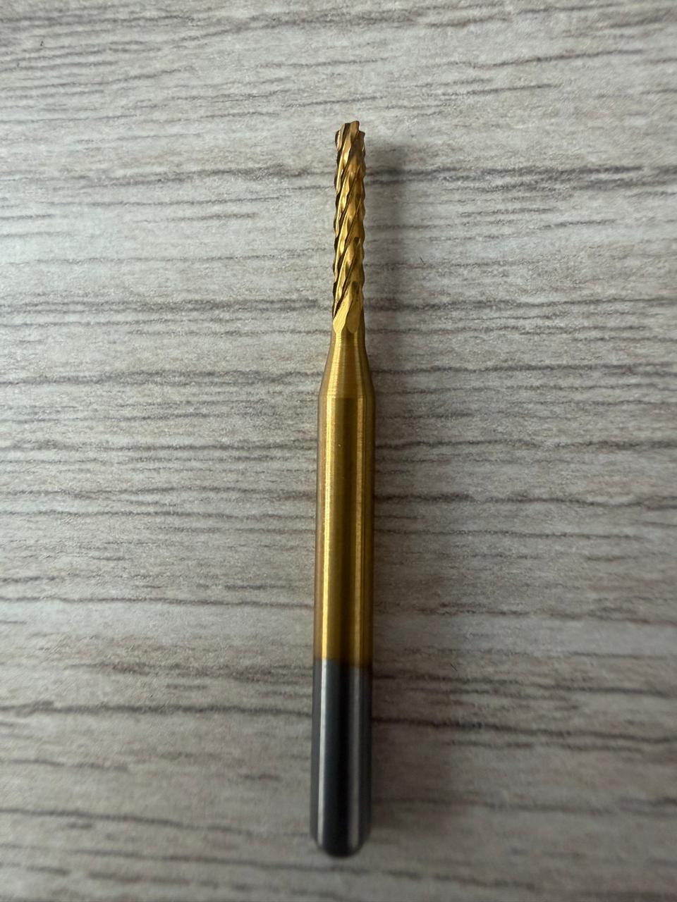
Used to cut the external contour of the PCB, allowing the board to be separated from the base material after the traces are engraved.
🪵 PCB Materials
Different materials can be used to fabricate printed circuit boards, each with different mechanical and thermal properties.
| Material | Code | Properties | Best For |
|---|---|---|---|
| Fiberglass | FR4 | High mechanical resistance, good structural stability, high durability | Professional boards — harder to machine, more tool wear |
| Phenolic Paper | FR1 | Easy to machine, less tool wear, clean copper engraving | ✅ Fab Lab rapid prototyping — widely used |
| Bakelite | — | Easy to machine, less resistant, can break, may not be uniform thickness | Simple prototypes with caution |
| Ceramic PCB | — | High heat resistance, brittle | High-temperature applications (soldering iron, hot air gun) |
💻 CAM Software
CAM software that converts Gerber files into CNC toolpaths. Used to generate engraving paths for PCB traces and prepare files for CNC machining.
- Convert Gerber → CNC toolpaths
- Generate isolation routing
- Configure milling parameters
Platform commonly used in Fab Labs to generate machine code and toolpaths. Includes a V-Bit Offset Calculator to determine correct cutting width based on tool angle and Z depth.
- Generate engraving & cutting paths
- Configure basic machining parameters
- V-Bit offset calculation
PCB Machining Process
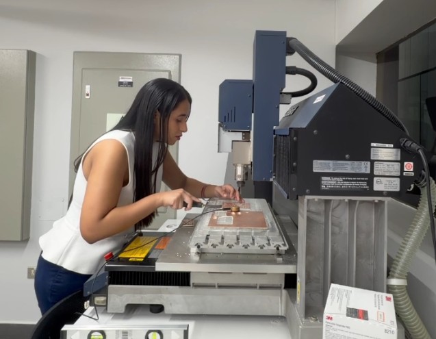
For this process, we used the Roland Modela Pro MDX-540 to machine FR1 (Phenolic Paper) PCB boards following a precise step-by-step workflow to ensure accurate engraving and clean board cutting.
⚙️ Step-by-Step Process
Cleaning and Preparation
Clean the workspace with alcohol and remove any debris. Prepare the copper board by adding double-sided tape to keep it flat and fixed to the sacrificial layer.
Placing the Board
Place the board on the sacrificial layer, ensuring it is well aligned and as flat as possible to guarantee uniform engraving depth across the entire surface.
Calibration
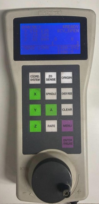
Set the origin considering the first quadrant (bottom to top, left to right). The control lets you move the X and Z axes to define the origin. For the Z-axis, use the Z0 SENSE option to adjust the tool height correctly.
Machining Process
Two settings are used: engraving and cutting. First, run the engraving G-code to trace the copper paths, and then run the cutting G-code to separate the board. This order avoids movement and loss of precision.
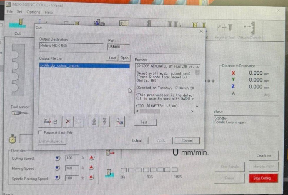
Running the Job — VPanel
Open VPanel for Modela Pro II on the computer, select the G-code file, and start the machine. Monitor the process until completion.
Final Step
Once machining is complete, carefully remove the PCB from the bed using a spatula, being careful not to bend or damage the board.
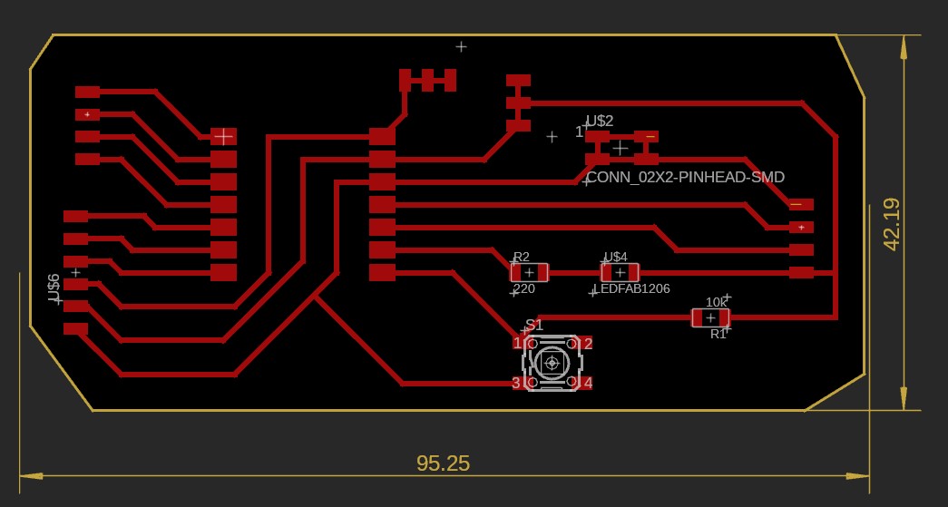
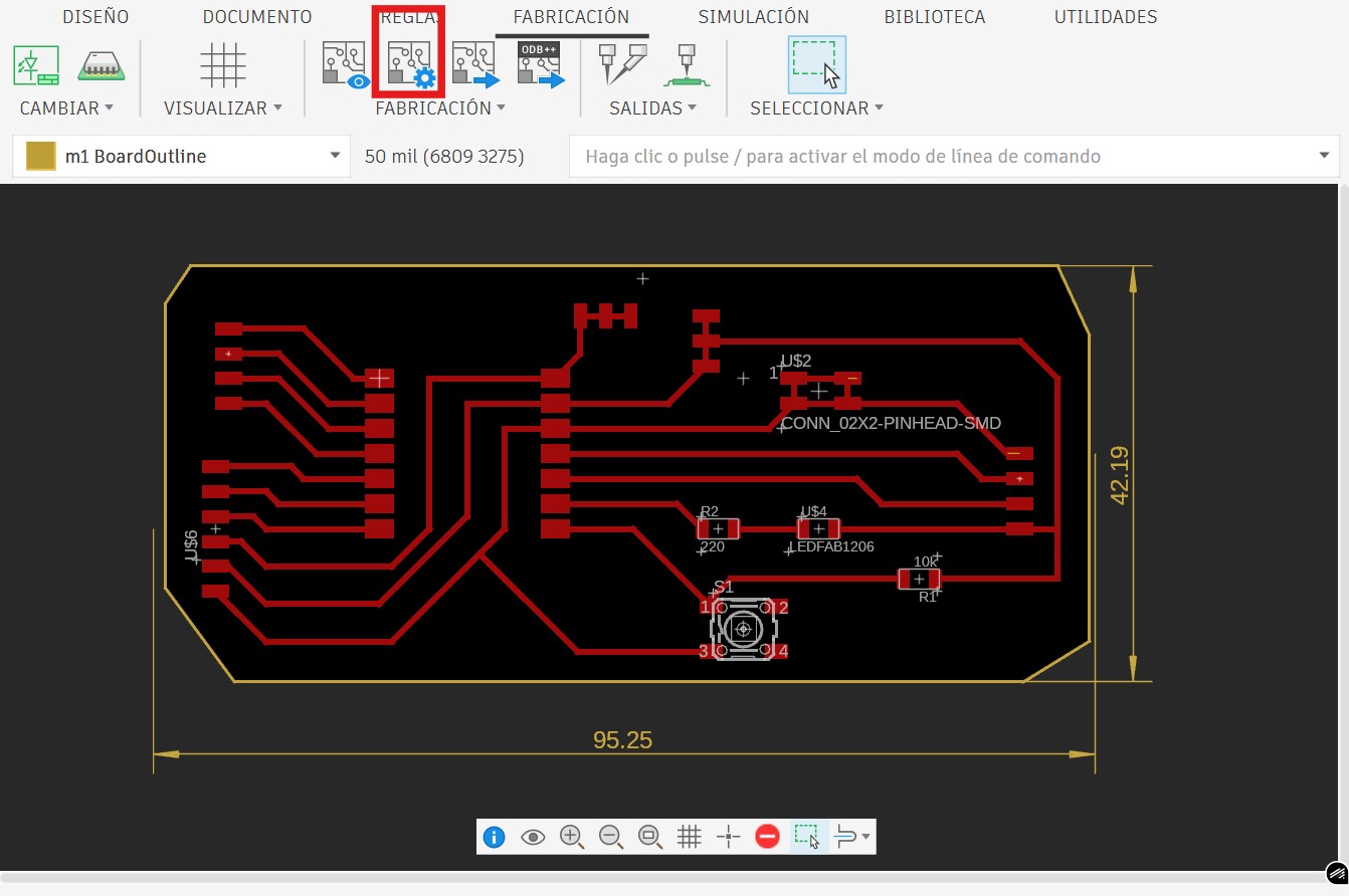
PCB Redesign
During Week 6, I designed my first PCB — but it wasn't good enough. For the Week 8 assignment, I decided to completely redesign the board. In the first version, I integrated many components directly on the PCB. After analyzing the circuit more carefully, I realized that several of these components could instead be connected using available free pins through headers.
Including them directly on the board was unnecessary and caused copper traces to cross each other, which could lead to fabrication problems during the milling process.
→ Go to Week 6: Electronics DesignBefore & After
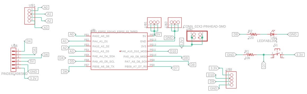
🗺️ Component Mapping
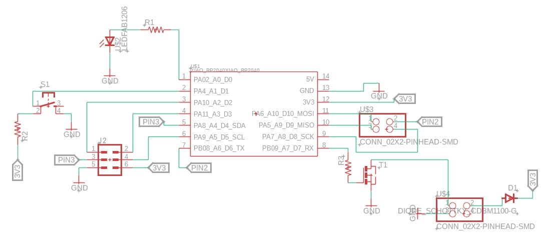
To redesign the PCB, I analyzed all the components and classified them according to their type and signal. The microcontroller used is the XIAO ESP32.
These sensors use digital pins, which operate with HIGH/LOW signals.
| Sensor | Qty | Function | Pin |
|---|---|---|---|
| IR / Proximity Sensor (HC-SR501) | 1 | Detect hand presence to activate the dispenser | D6 |
| Optical sensors (per compartment) | 3 | Detect stock level in each compartment | Digital header |
| Power On/Off Button | 1 | Turn the device on or off | D7 |
| Motor Encoder | 1 | Count the position of the dispensing mechanism | Digital header |
Analog sensors use ADC pins, which read variable signals.
| Sensor | Qty | Function | Pin |
|---|---|---|---|
| Load Cell (HX711) | 1 | Measure stock weight in one compartment | A0 (Analog header) |
These components generate the mechanical movement of the system.
| Component | Qty | Signal Type | Pin |
|---|---|---|---|
| Servo Motors | 3 | Digital PWM | D9, D10 |
| DC Motor | 1 | Digital (motor driver L298N or DRV8833) | External driver |
These components provide visual feedback to the user.
| Component | Qty | Interface | Pin |
|---|---|---|---|
| LCD Display | 1 | I2C (SDA / SCL) | SDA, SCL |
| LED Strip (WS2812B) | 1 | Digital data signal | Digital header |
| Status LED | 1 | Digital | D8 |
The PCB includes several headers to simplify external connections.
| Header | Connector | Pins |
|---|---|---|
| Button | Direct connection | D7 + 1kΩ resistor + GND |
| Status LED | Direct connection | D8 + 330Ω resistor + GND |
| 5V Power | 1×3 | 5V, 5V, 5V |
| GND | 1×3 | GND, GND, GND |
| 3.3V Power | 1×3 | 3.3V, 3.3V, 3.3V |
| Analog Pins | 1×4 | A0, A1, A2, A3 |
| Digital Header 1 | 1×5 | SDA, SCL, D6, 3.3V, GND |
| Digital Header 2 | 1×4 | D9, D10, 3.3V, GND |
Pin Requirement Summary
4–5 pins required for sensors, button, and LED.
1 pin for the load cell (HX711).
2 pins for servo motor control.
2 pins for LCD display communication.
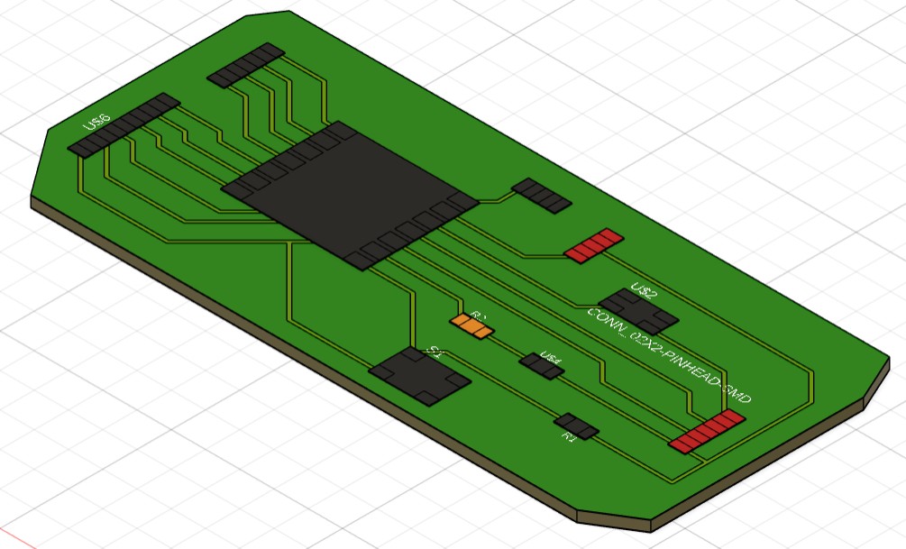
🖥️ PCB Design Views

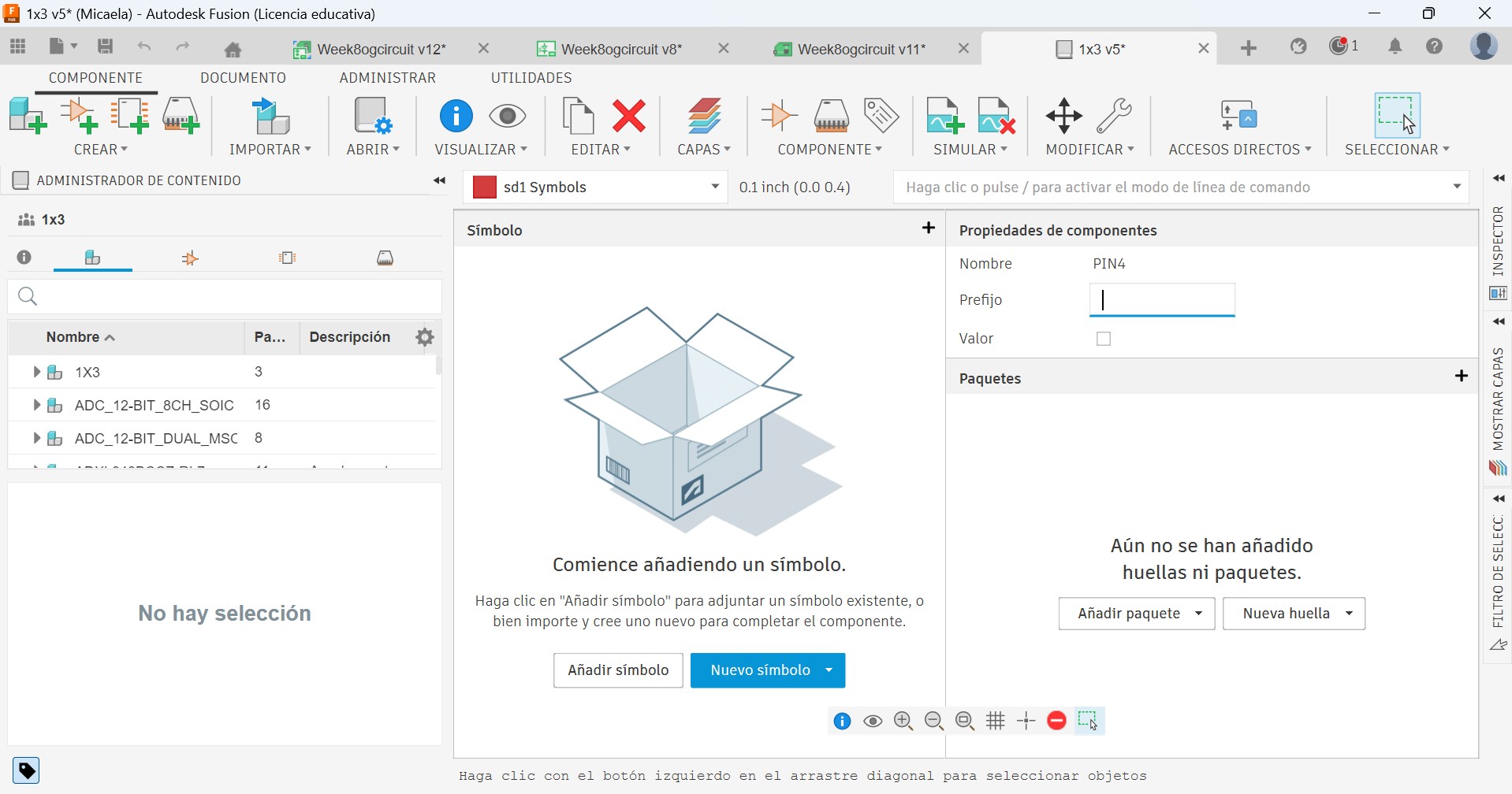
🔧 Creating SMD Components in Fusion 360
The same procedure was followed to create three SMD pin connectors: 1×3, 1×4 and 1×6. Each one went through the same four steps described below.
Configure Component Properties
The component editor opens where the Name and Prefix fields are filled in on the right panel. The Añadir símbolo button is pressed to link an existing symbol and Nueva huella to create the footprint.
Verify Symbol and Associate the Footprint
The left panel shows the component structure in three levels: component, symbol and footprint. Each part can be edited separately by clicking on it.
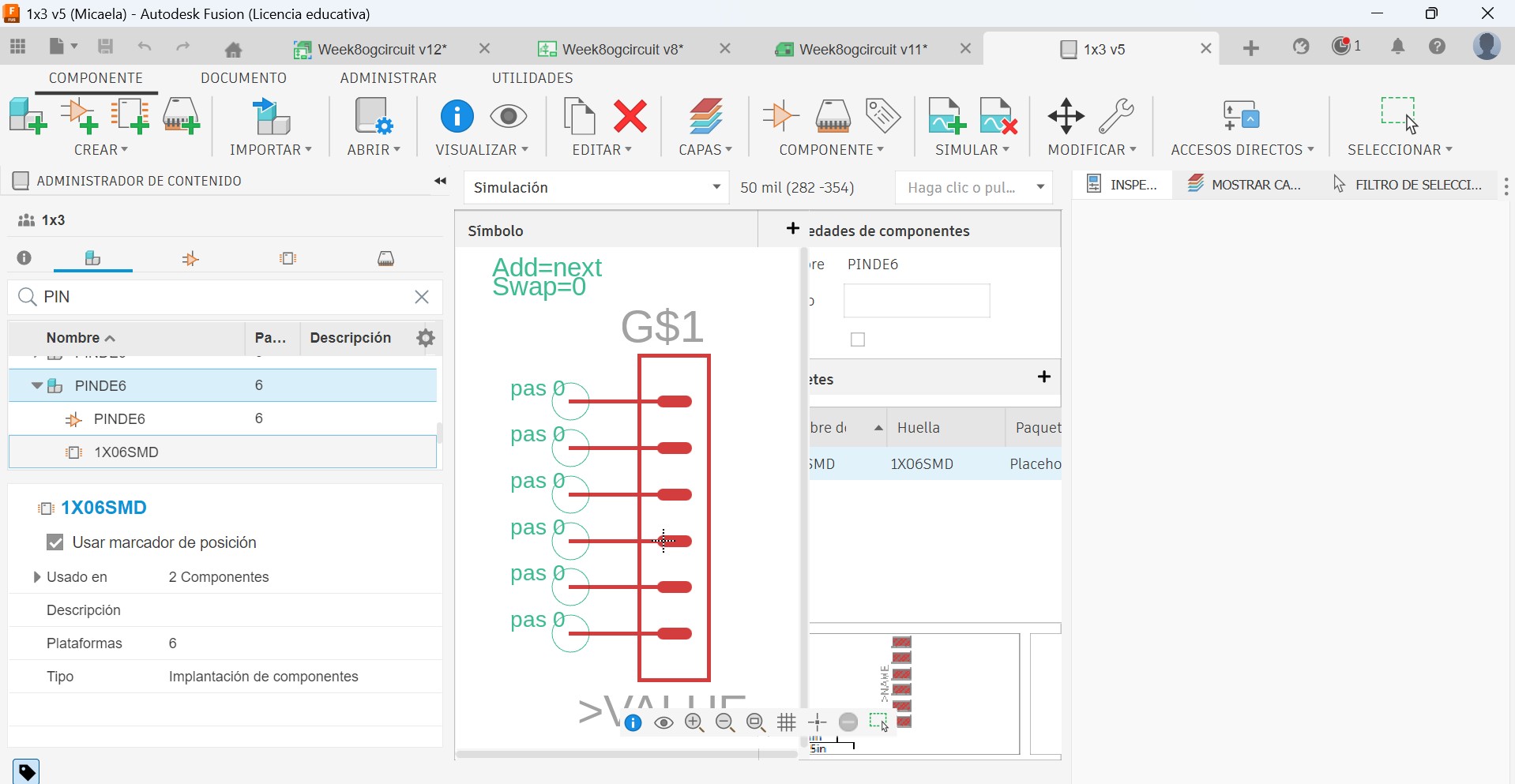
Edit the Footprint in the Footprint Editor
Fusion 360 automatically switches to the HUELLA tab, where the 6 SMD pads are visible, numbered 1 to 6, vertically aligned on the top copper layer.
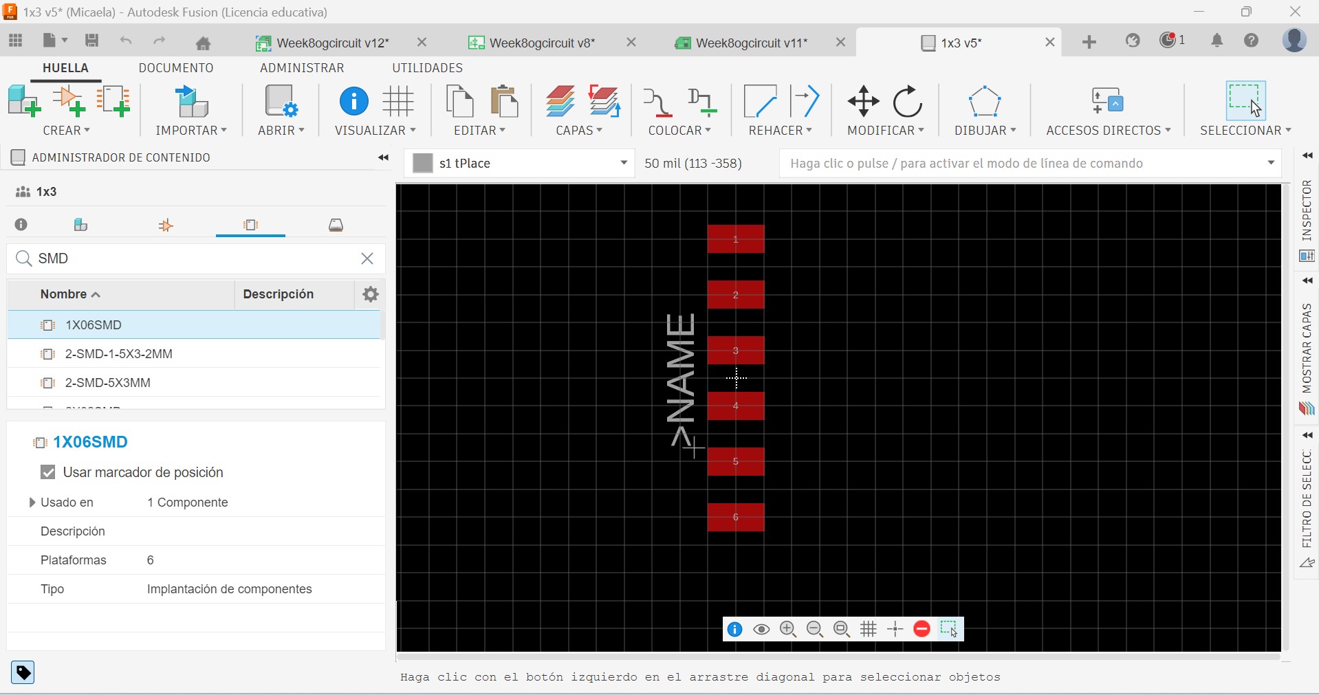
Link Pins to Pads
The Connect 1X06SMD window opens showing three columns: Pin, Platform and Connection. The Conectar button is pressed six times — once per pin — to complete the mapping. Finally Aceptar is pressed and the component is ready to use in the PCB design.
📁 Exporting Gerber Files from Fusion 360
In Autodesk Fusion 360, go to the Manufacture tab and select the CAM Processor. From there, click on "Generate Gerber Files".
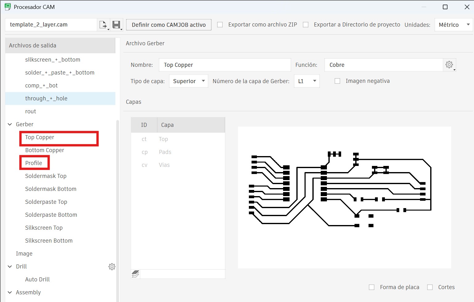
Save the files in an empty folder. Automatically, all the necessary files are generated. The most important ones are:
Used for engraving the traces — contains all the circuit paths to be milled into the copper layer.
Used for cutting the board outline — defines the external contour that separates the PCB from the base material.
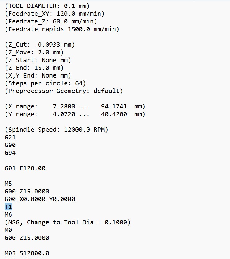
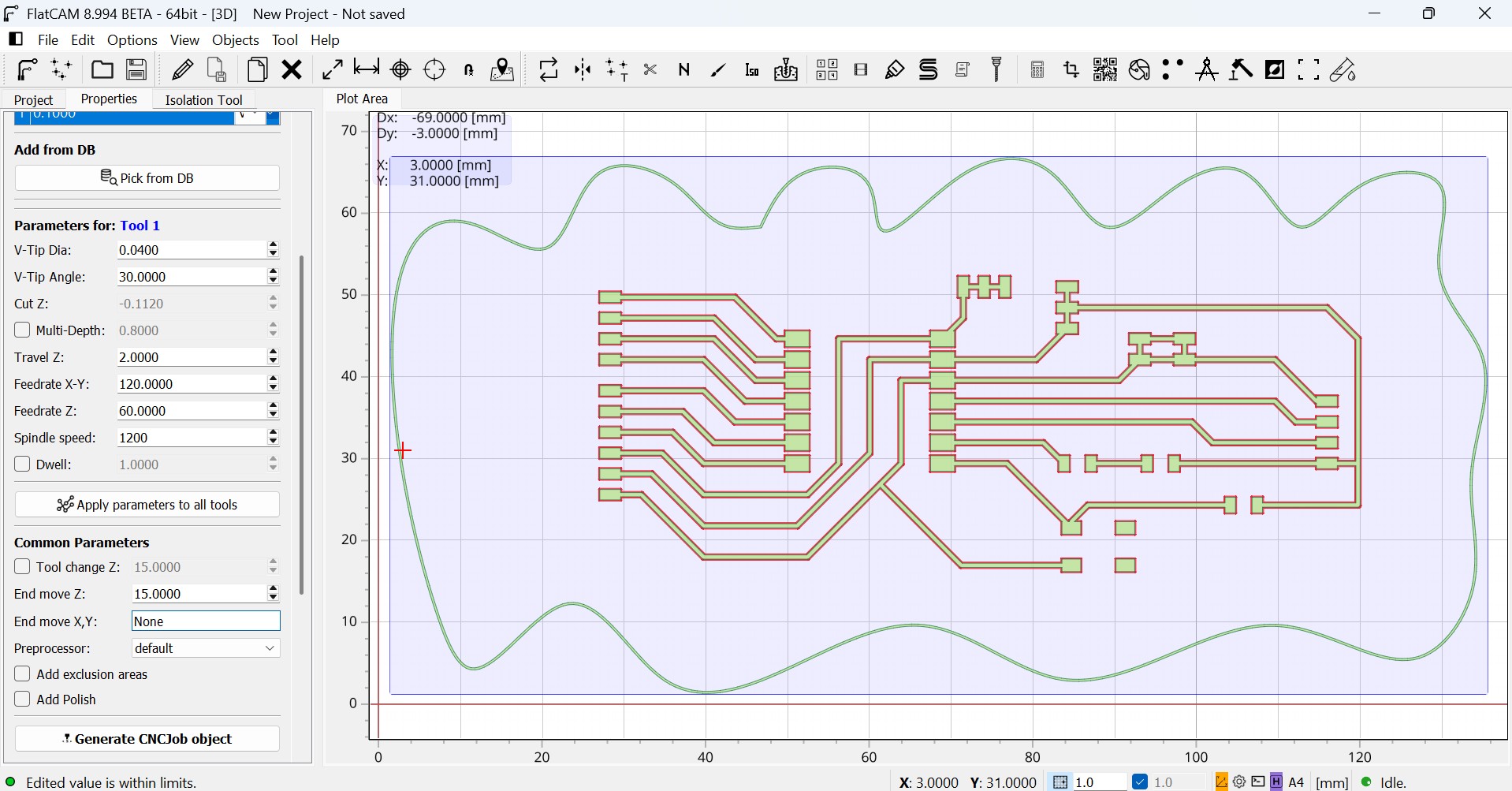
⚙️ Generating Toolpaths with FlatCAM
Since the PCB design was created in Autodesk Fusion 360, the files were exported as Gerber files. For the individual assignment, I used FlatCAM to generate the G-code for the CNC milling machine.
- Import the
.gbr(Gerber) file into FlatCAM. - Move the Gerber design to the center axis.
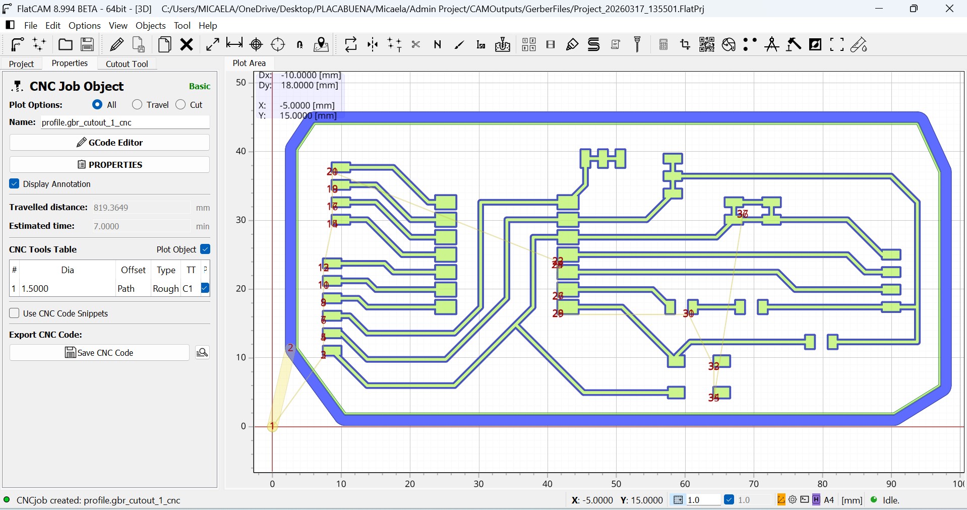
- Generate the isolation routing for the copper traces.
- Configure the milling parameters: tool diameter, tip angle, and spindle speed.
- Generate the CNC object after the routing is created.
- Export the final G-code for the machine.
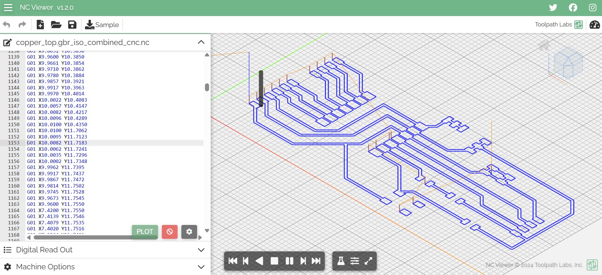
Then, I simulated the G-code using NC Viewer at ncviewer.com, which allowed me to visualize the cutting layers and verify that there were no extra paths or unwanted dots in the design.
Milling, Soldering & Programming
🛠️ Material & Equipment Used
For this individual assignment, I fabricated the PCB using the following specifications:
FR1 (Phenolic Paper) — A safe, easy-to-machine material suitable for rapid prototyping on lab equipment.
Roland Modela Pro II MDX-540 — Precision CNC milling machine at Fab Lab ULima, optimized for FR1 and other soft materials.
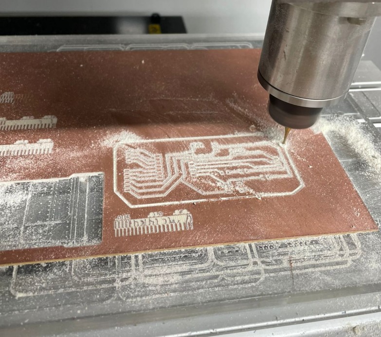
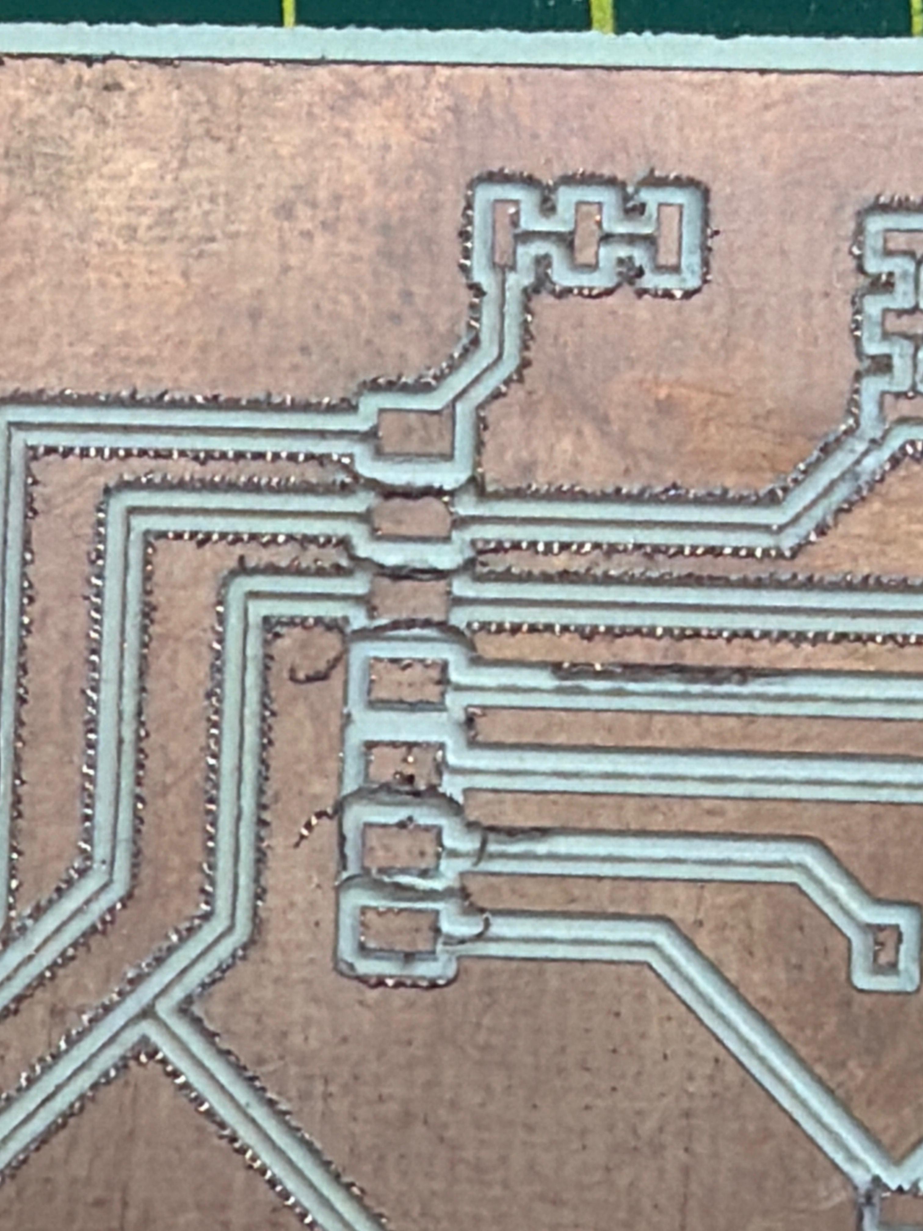
🏭 Milling the PCB
The PCB milling process consists of two main steps: engraving the copper traces and cutting the board outline. Both operations were performed on FR1 (Phenolic Paper) using the Roland Modela Pro II MDX-540 using the G-code files generated in FlatCAM.
Board Preparation & Setup
Clean the FR4 copper board with alcohol and secure it to the sacrificial layer using double-sided tape. Ensure the board is flat and well-aligned on the machine bed.
Machine Calibration
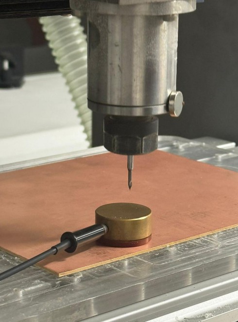
Set the X and Y origin at the corner of the board. Use the Z0 SENSE function to calibrate the Z-axis height accurately — this is critical for consistent trace width during engraving.
Engraving the Traces
Load the engraving G-code (copper top layer) into VPanel and start the machine. The V-bit tool traces all circuit paths into the copper, creating isolated signal lines. This step took approximately 15–20 minutes.
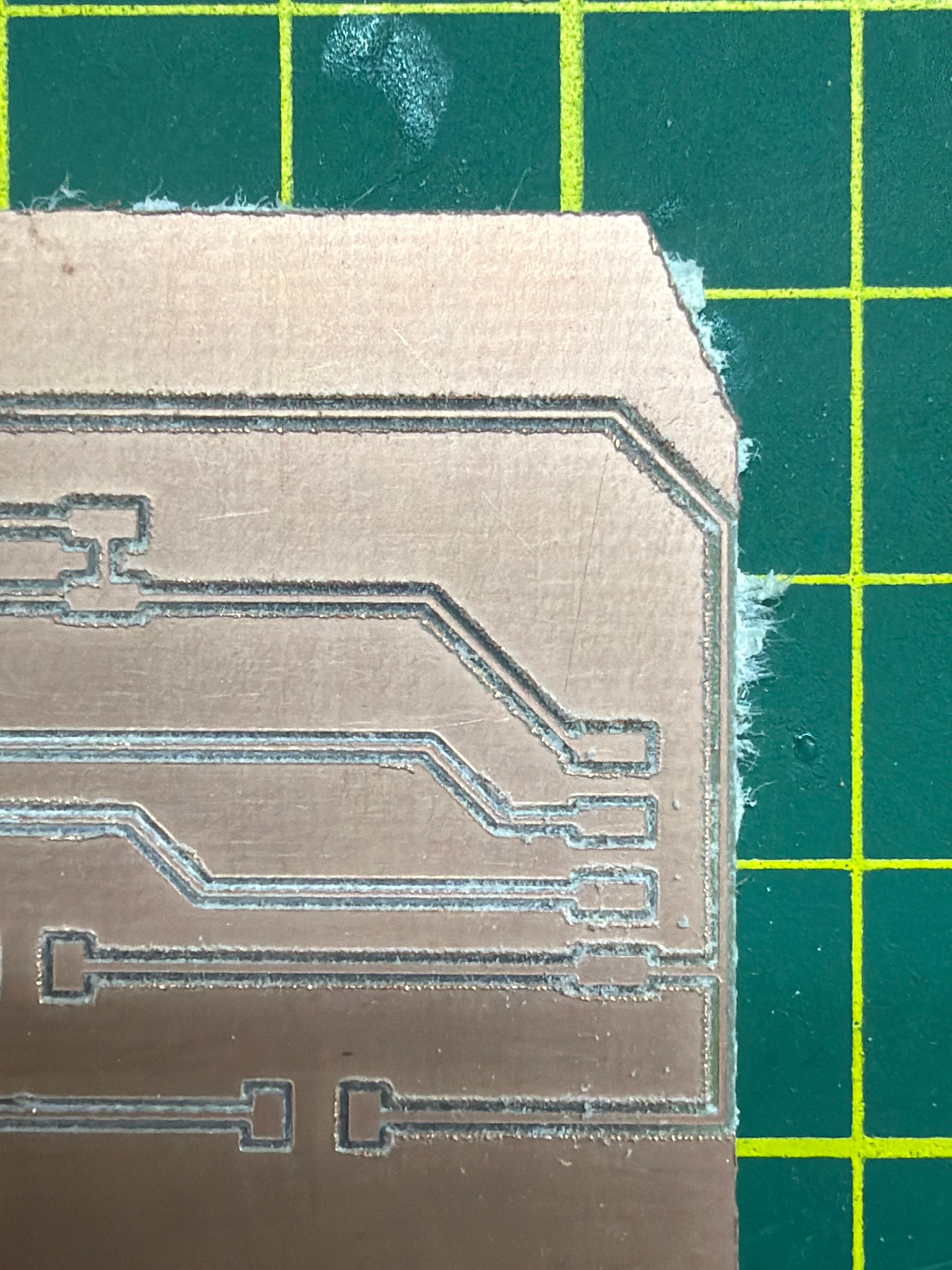
Cutting the Board Outline
After engraving completes, load the cutting G-code (profile/outline) and run the flat end mill tool. This separates the PCB from the sacrificial layer, creating clean edges.
Removing the Board
Once milling is complete, carefully remove the board using a spatula, being careful not to bend or damage the freshly milled traces.
🧪 Fabrication Tests
In the ceramic test, the traces ended up being too thin. This happened because we used a very sharp milling bit, and during the Z-axis calibration, since the material is brittle, the tool went slightly deeper than expected and removed more material from the traces. Because of this, some of the paths became too narrow, which could affect the connectivity of the circuit.
The fiberglass test had a better finish with cleaner, more consistent trace widths.
Traces too thin due to brittle material and deeper-than-expected Z penetration.
Better finish with consistent trace widths and clean copper engraving.
🔥 Soldering & Assembly
After successfully milling the PCB, the next step was to populate the board with components and solder them securely. All components were soldered by hand using a traditional soldering iron.
- XIAO ESP32-C3 microcontroller
- Power button with pull-down resistor (10kΩ)
- Status LED with current-limiting resistor (330Ω)
- Decoupling capacitor (100µF) for stable power supply
- Multiple header connectors (1×3, 1×4, 1×5, 1×6) for external sensors and modules
Each component pad was heated with the soldering iron tip, and solder was applied to create a strong mechanical and electrical bond. Care was taken to:
- Avoid cold solder joints (which break easily)
- Keep solder away from adjacent traces to prevent shorts
- Ensure proper heat distribution to avoid damaging components
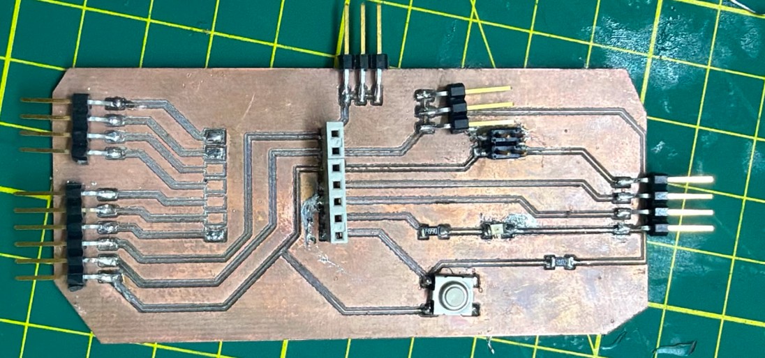
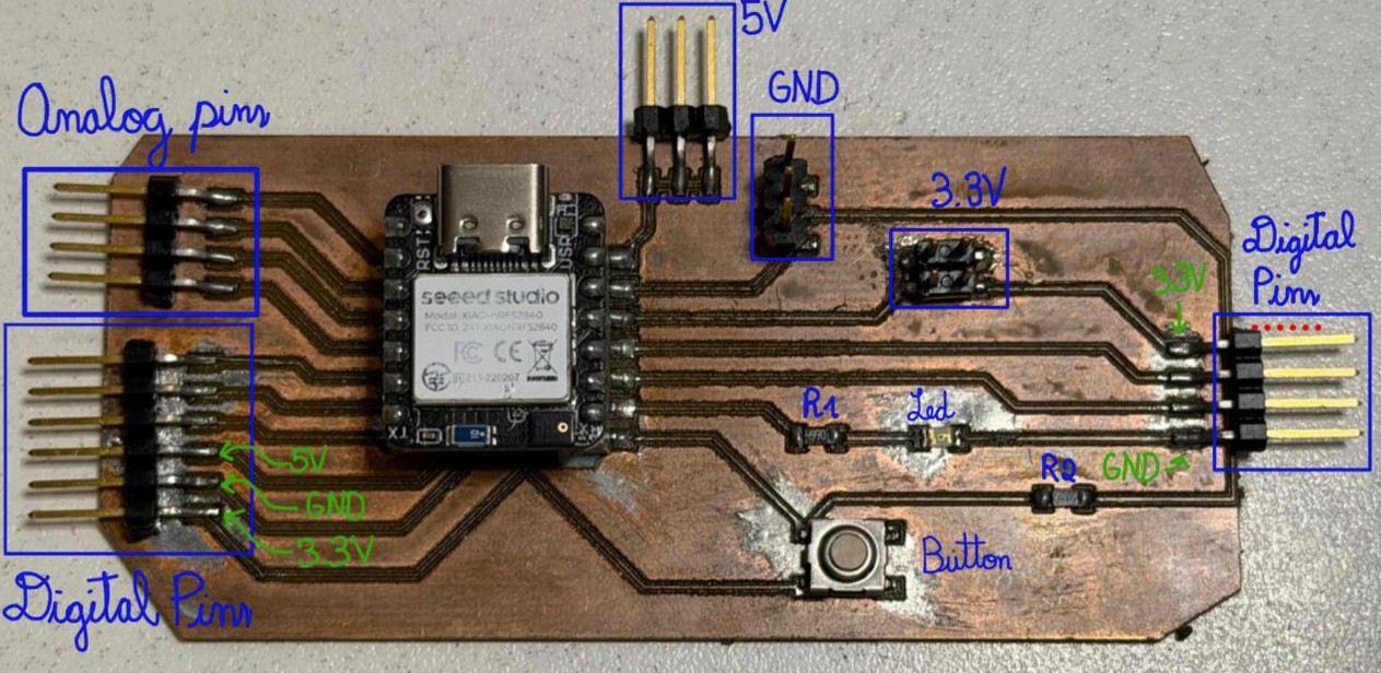
The final soldered board features all essential components neatly arranged and securely attached. The headers are clearly visible and ready to accept external sensor modules.
🧪 PCB Testing & Verification
Before uploading code, the board was tested to ensure all solder joints were good and there were no shorts or broken connections.
A multimeter was used to check continuity of critical traces and verify proper electrical connections between components.

💻 Programming & Functionality Testing
The following code was uploaded to the board to test the basic LED + sensor functionality. The code reads a distance sensor and controls the onboard LED.
#include <Adafruit_TinyUSB.h>

// HC-SR04 Ultrasonic Sensor Pins
const int TRIG = D9;
const int ECHO = D10;

// Onboard Status LED
const int MY_LED = 8;

void setup() {
  pinMode(TRIG, OUTPUT);
  pinMode(ECHO, INPUT);
  pinMode(MY_LED, OUTPUT);
  digitalWrite(MY_LED, LOW);  // LED off at startup
}

void loop() {
  // Trigger ultrasonic pulse
  digitalWrite(TRIG, LOW);
  delayMicroseconds(2);
  digitalWrite(TRIG, HIGH);
  delayMicroseconds(10);
  digitalWrite(TRIG, LOW);

  // Measure echo time
  long duration = pulseIn(ECHO, HIGH);
  float distanceCM = (duration * 0.034) / 2;

  // LED logic: ON if object detected close
  if (distanceCM < 10) {
    digitalWrite(MY_LED, HIGH);  // Hand close — LED ON
  } else {
    digitalWrite(MY_LED, LOW);   // No detection — LED OFF
  }

  delay(100);
}
✅ Board is fully functional! The LED responds correctly to object proximity:
- When an object (hand) is brought within 10cm, the LED illuminates
- When the object moves away, the LED turns off
- Response time is immediate with no latency
Below is a video showing the completed board with the status LED responding to proximity sensor input: