
What is an EDA Tool?
An EDA Tool (Electronic Design Automation Tool) is software used to design, simulate, and analyze electronic circuits and PCBs. These tools allow engineers to create schematics, design board layouts, verify electrical connections, and generate manufacturing files.
EDA tools are essential in modern electronics because they reduce design errors, improve precision, and speed up the development process. Commonly used tools include KiCad, Altium Designer, EAGLE, and Fusion 360.
Designing a development board means creating a PCB centered around a microcontroller for prototyping and testing. It covers schematic design, component selection, PCB layout, and design rule verification — then the board can be programmed for specific tasks, connecting with the embedded programming work from Week 4.
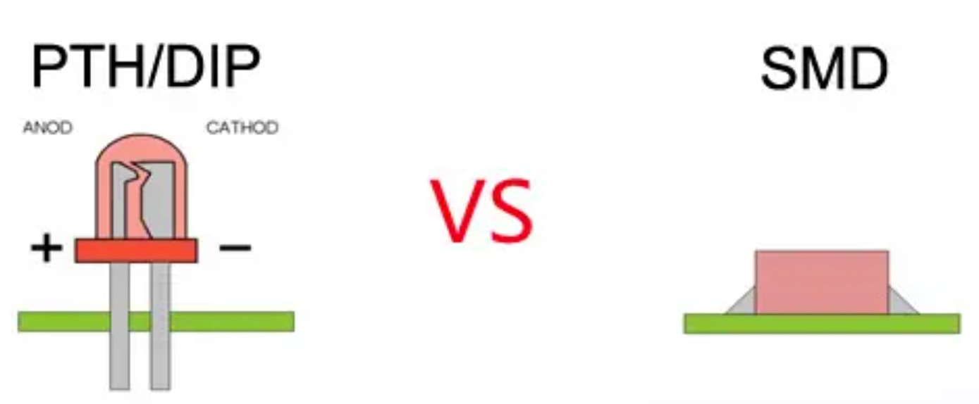
→ Go to Week 4: Embedded ProgrammingThrough-Hole Technology (THT) passes components through drilled holes for strong mechanical support. Surface Mount Technology (SMT) mounts SMD components directly on the surface, enabling smaller designs. In Fab Academy, we primarily use SMD components.
Embedded Programming Components
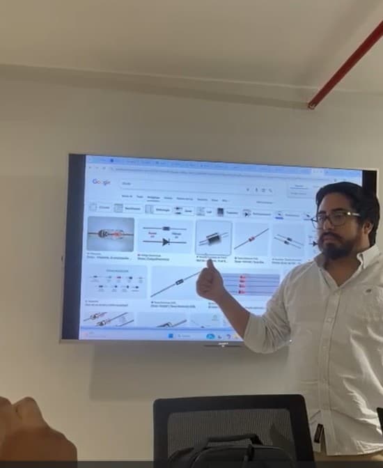
With our instructor, we reviewed the main components of embedded programming — resistors, diodes, transistors, inductors, and push buttons — focusing on their function and interaction within a circuit.
Key Components
- Resistors (110 Ω) — Not polarized. Limit current and protect components.
- LED — Polarized (anode/cathode). Requires a resistor to prevent burnout.
- Transistor — Electronic switch with emitter (E), collector (C), base (B). Fundamental for logic gates.
- Diode — Allows current in one direction only. Protects the microcontroller.
- Inductors — Store energy as a magnetic field.
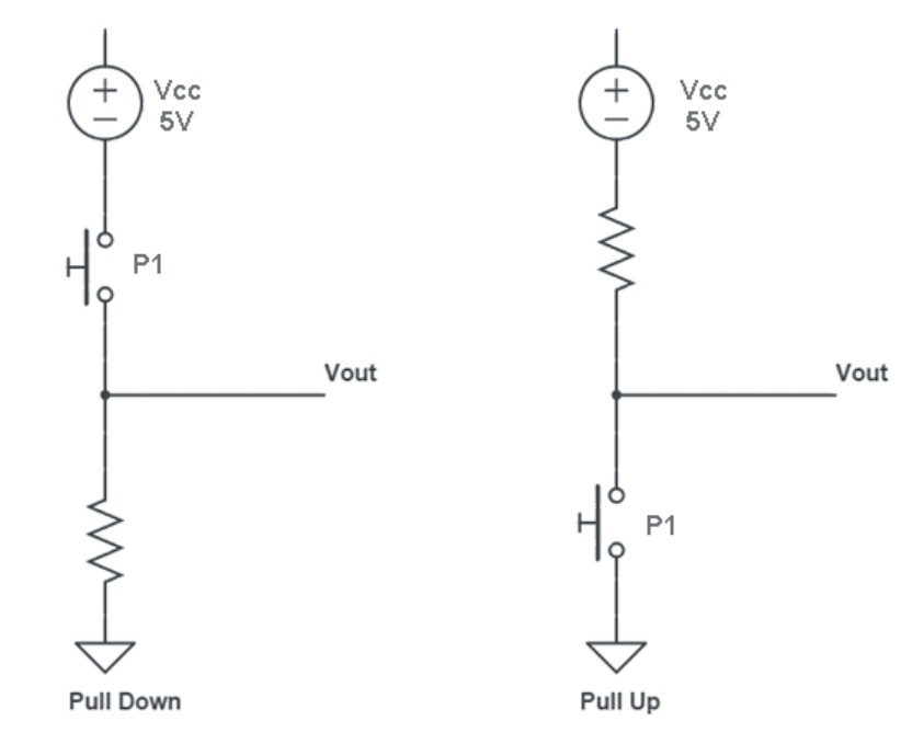
Push Button & Pull-Down Resistor
Without a resistor, a button input becomes a floating point — unstable, randomly reading HIGH or LOW. A pull-down resistor (10 kΩ) to ground ensures LOW when not pressed, HIGH when pressed.
Lab Equipment & Electrical Concepts
My Group Contribution: Together with my lab group, we characterized the functionality of fundamental lab equipment including the Prasek Premium PR-85 multimeter and the Siglent SDS 1102CML+ oscilloscope. I documented the DC voltage measurements on various components, led the experiments testing LEDs under different voltage conditions, and recorded the PWM signal behavior analysis on the oscilloscope.
Click each concept to expand its formula and explanation.
Voltage is what "pushes" current through the circuit — energy per unit charge between two points.
Flow of electric charge over time. We use conventional current (positive → negative), while electrons physically move in reverse.
Higher resistance means less current for the same voltage.
Stores energy in an electric field. A stable DC voltage means zero capacitor current — current only flows when voltage is changing.
Stores energy in a magnetic field. Opposes sudden changes in current.
🔌 Multimeter — Prasek Premium PR-85
The Prasek Premium PR-85 is a digital multimeter that allows measuring different electrical quantities and verifying whether components are working correctly. Each function below is color-coded to match the physical device dial — click any to expand.
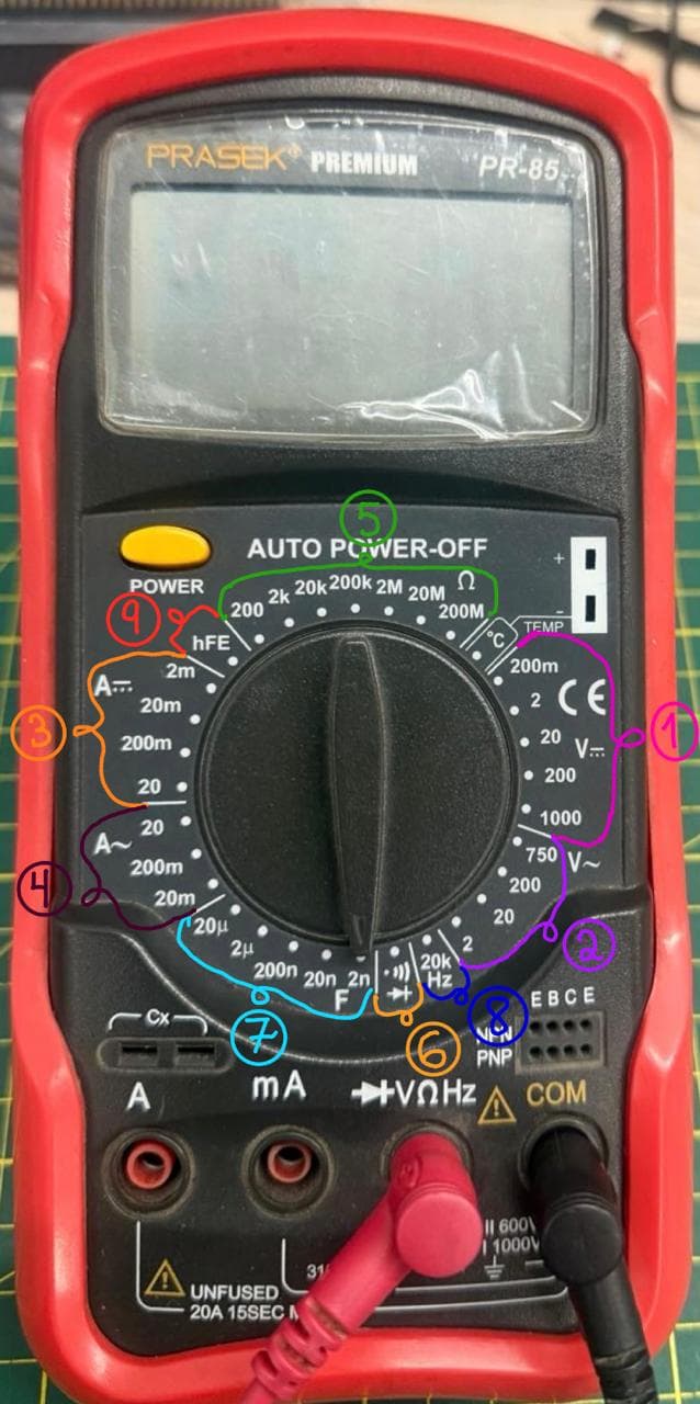
Scales: 200 mV · 2 V · 20 V · 200 V · 1000 V
Used to measure: voltage from regulated supplies, microcontroller output, LEDs, sensors, etc.
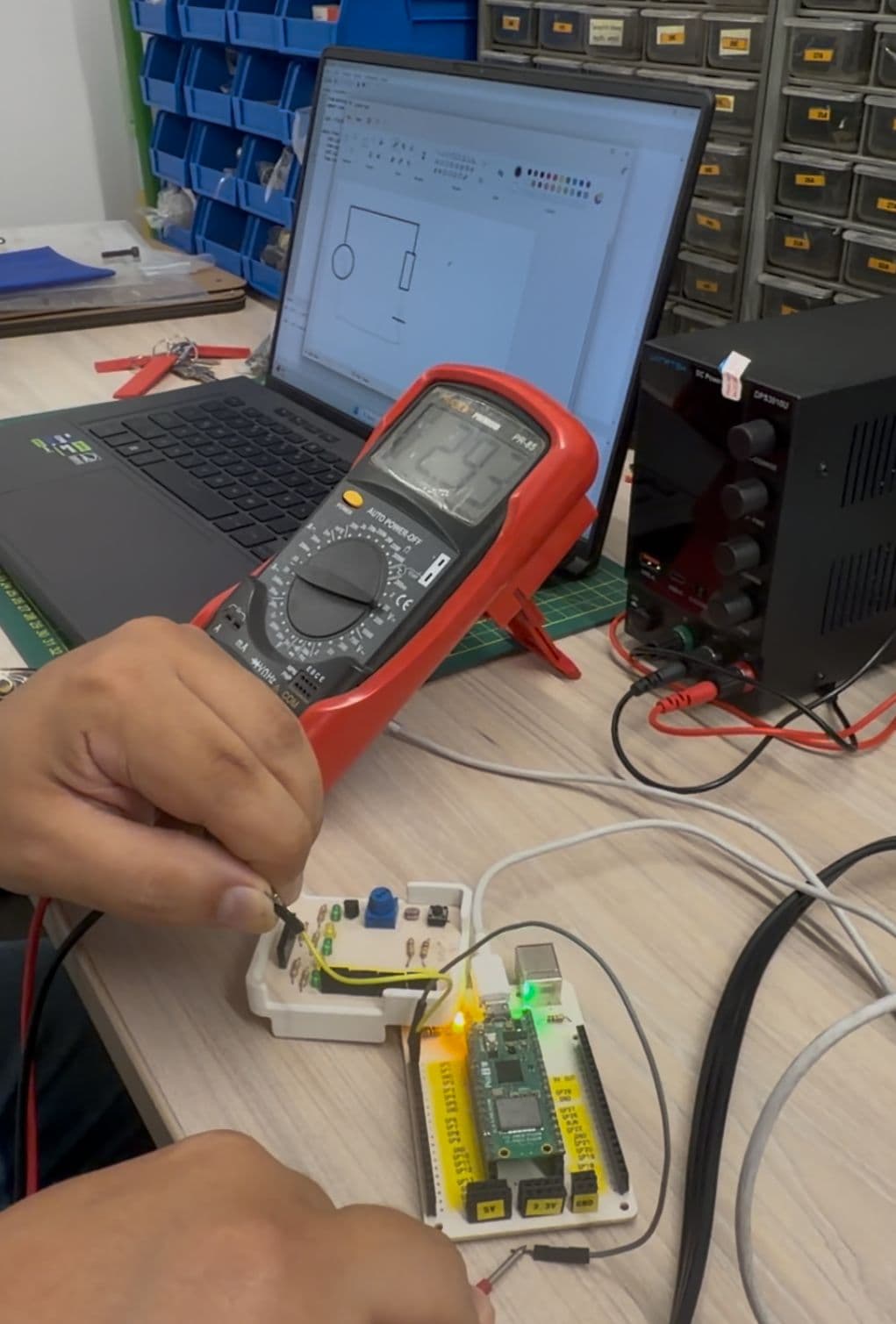
Our experiment: Placed in series with the yellow LED, at the 20 V range, we read approximately 2.93 V being supplied to the LED — dropping to zero when the microcontroller turned the LED off. Although the microcontroller runs at 3.3 V, this lower reading indicates the connected GPIO pin is worn and doesn't supply its full rated voltage.
Scales: 200 V · 750 V
Used to measure alternating current, such as the electrical grid. This mode is for high-voltage AC sources only — not for microcontroller circuits.
Scales: 20 µA · 200 µA · 2 mA · 20 mA · 200 mA
Used to measure the consumption of small components such as LEDs or sensors.
Scales: 20 mA · 200 mA · 20 A
Measures alternating current in equipment or systems that run on AC. As with DC current, the multimeter must be connected in series with the circuit.
Scales: 200 Ω · 2k · 20k · 200k · 2M · 20M
Used to measure resistors, verify components, and detect open circuits.
🔬 LDR Experiment: We tested an LDR using the 200 kΩ scale in three conditions:
- Fully covered (total darkness): High resistance reading
- Ambient room light: Resistance decreased
- Direct light applied: Resistance dropped even further
This confirmed the LDR increases resistance in darkness and reduces it with more light — validating its function as a light-dependent sensor.
This function is found on the same selector position as the diode symbol. It does not work with a numerical scale — it is a quick verification tool.
When there is a connection between two points and the resistance is very low, the multimeter emits a beep. Used to verify that a trace or cable is properly connected.
Diode Test ➤|— Verifies that a diode conducts in only one direction and measures its forward voltage drop. Very useful for identifying anode and cathode before soldering:
- Black probe → Cathode
- Red probe → Anode
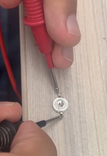
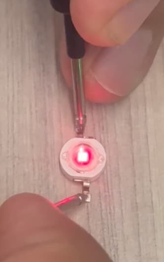
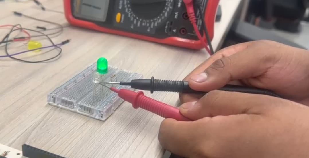
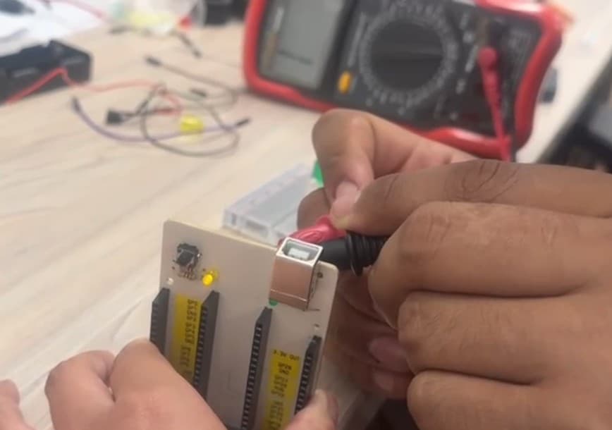
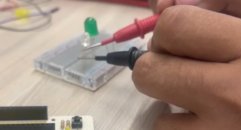
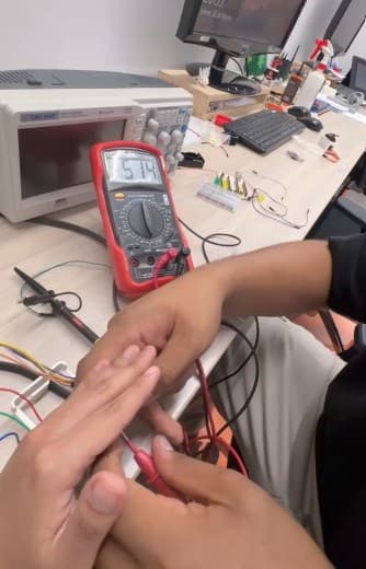
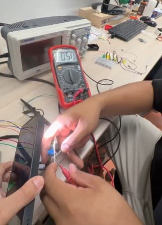
💡 LED Experiment — SMD vs THT: We tested green SMD and transparent THT LEDs on a breadboard. To light a LED, the Black probe must go to the Cathode and the Red probe to the Anode. We observed that the voltage the multimeter provides in diode test mode (~2.7 V) is not enough to light the transparent LED, but it does light the SMD green ones.
Scales: 20 nF · 200 nF · 2 µF · 20 µF
Measures the value of a capacitor and verifies whether it is in good condition.
Range: Up to 20 kHz
Measures the frequency of electrical signals. For analyzing PWM signals it is more recommended to use an oscilloscope, as it also shows waveform shape and duty cycle visually.
Includes ports for both NPN and PNP transistors.
Measures the current gain (hFE) of a transistor and verifies that it is functioning correctly. Useful for confirming transistor type and checking for damaged components before soldering.
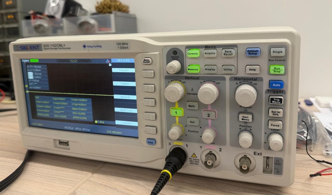
📺 Digital Oscilloscope — Siglent SDS 1102CML+
Unlike the multimeter, the oscilloscope visualizes how voltage changes over time. Y-axis = voltage · X-axis = time. The trigger system stabilizes the signal for clean analysis.
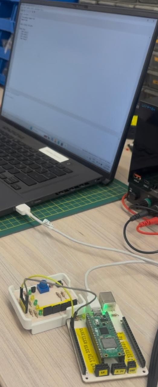
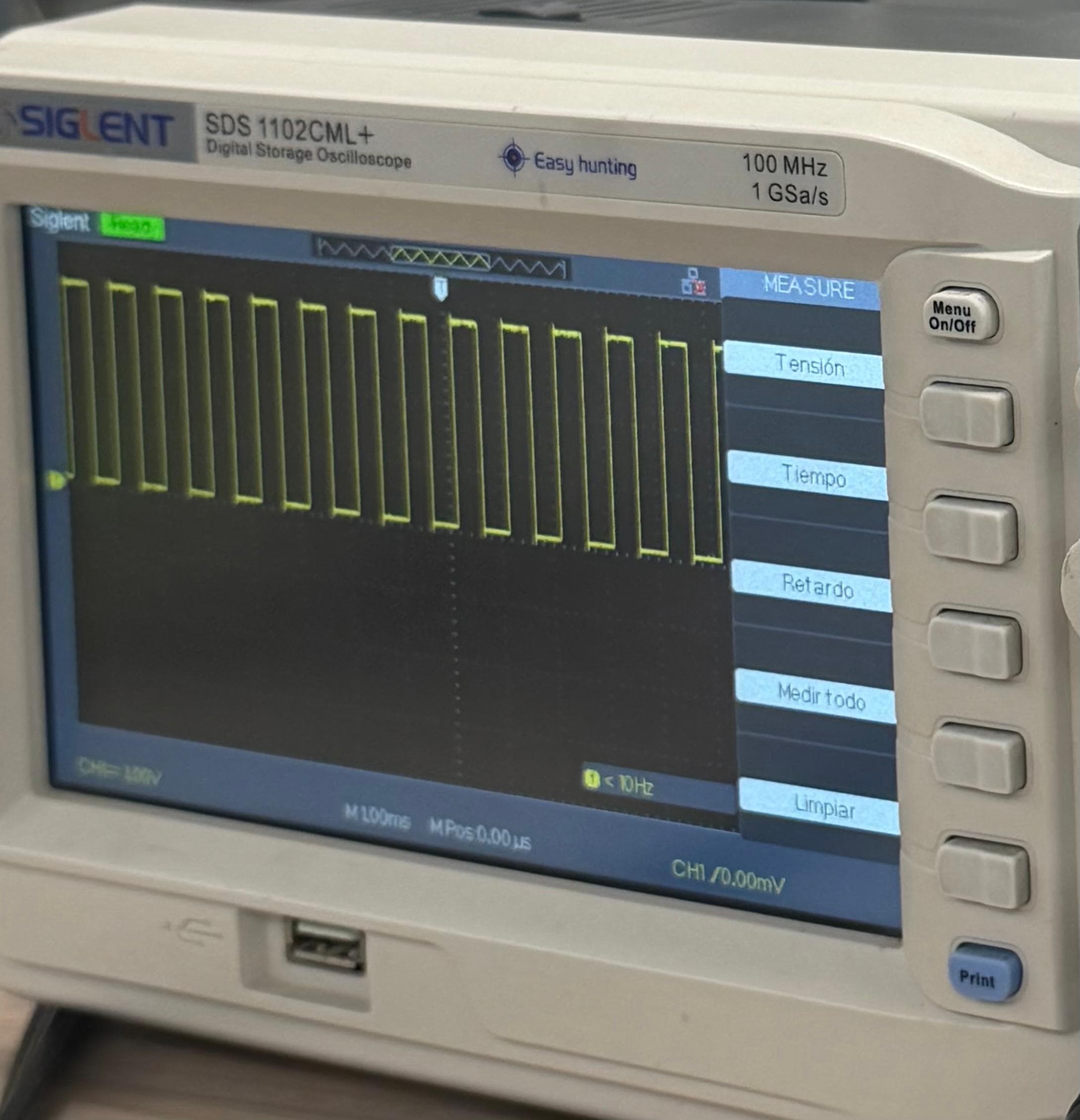
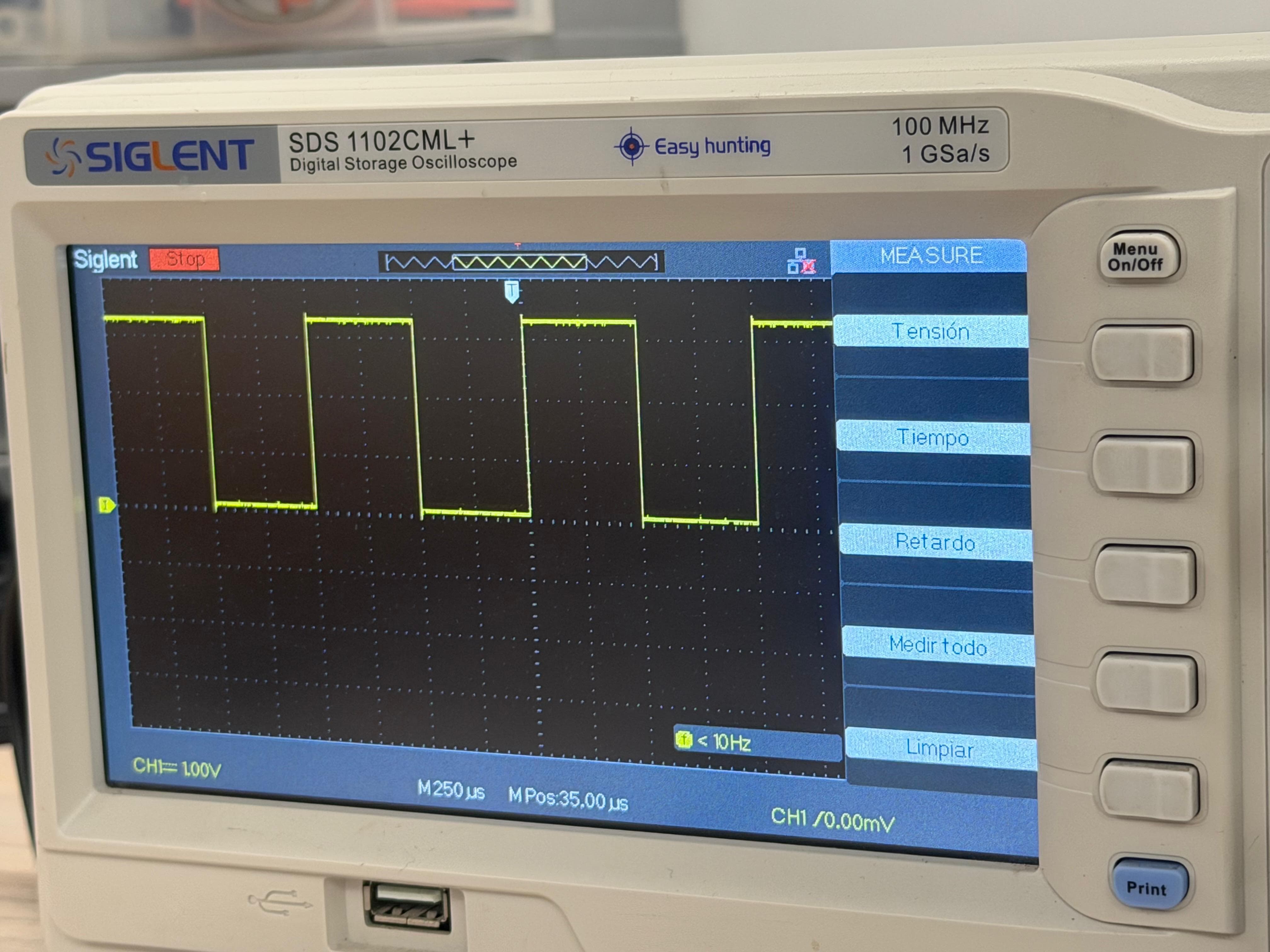
We built a test circuit with a Raspberry Pi Pico W2 and an LED, controlling it via PWM programmed in Thonny:
A low duty cycle (5%) produces short PWM pulses:
A high duty cycle produces longer PWM pulses:
Multimeter Voltage on the Oscilloscope
The oscilloscope detected the multimeter providing ~2.7 V during diode test mode — explaining why components requiring more than 2.8 V won't activate.
PWM is a digital technique controlling power by rapidly switching between HIGH (on) and LOW (off). On the oscilloscope you see the square waveform, period, frequency, and duty cycle. Used to control motor speed, regulate LED brightness, and simulate analog output.
The duty cycle is the percentage of time the signal is HIGH within one full period.
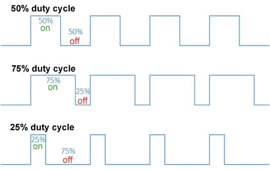
- 50% → equal on/off time
- Higher % → more average power → LED brighter
- Lower % → less average power → LED dimmer
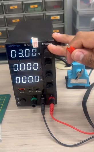
⚡ Regulated Power Supply — Wanptek DPS3010U
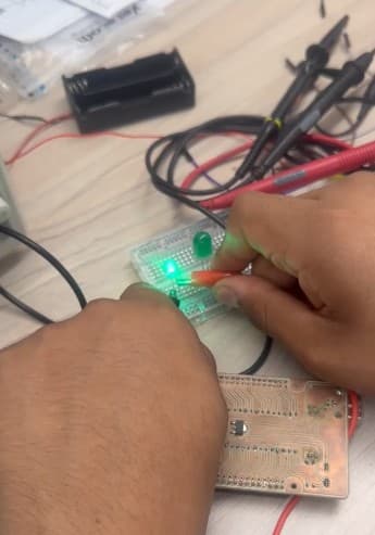
Variable voltage (0–30 V) and adjustable current (0–10 A). Shows consumed current in real time for safe testing. We found the transparent LED's turn-on threshold: 3 V.
Supporting Elements
- Voltage divider — Steps down voltage using resistors (e.g., 12 V → 5 V for a sensor).
- Electrolytic capacitor — Cylindrical, polarized. Filters voltage variations and reduces electrical noise.
Circuit Simulation
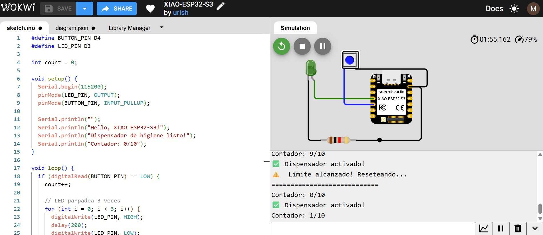
I used a 6mm push button and a green LED on the XIAO ESP32-S3. The button simulates each towel dispense — every press blinks the LED and increments a counter. At 10 presses, the system warns that towels have run out and resets automatically.
Code
#define BUTTON_PIN D4
#define LED_PIN D3

int count = 0;

void setup() {
  Serial.begin(115200);
  pinMode(LED_PIN, OUTPUT);
  pinMode(BUTTON_PIN, INPUT_PULLUP);
  Serial.println("Hello world!");
  Serial.println("Hygiene dispenser ready!");
  Serial.println("Counter: 0/10");
}

void loop() {
  if (digitalRead(BUTTON_PIN) == LOW) {
    count++;
    // LED blinks 3 times as confirmation
    for (int i = 0; i < 3; i++) {
      digitalWrite(LED_PIN, HIGH);  delay(200);
      digitalWrite(LED_PIN, LOW);   delay(200);
    }
    if (count >= 10) {
      Serial.println("✅ Dispenser activated!");
      Serial.println("⚠️  Limit reached! Resetting...");
      count = 0;
      Serial.println("Counter: 0/10");
    } else {
      Serial.println("✅ Dispenser activated!");
      Serial.print("Counter: ");
      Serial.print(count); Serial.println("/10");
    }
    delay(500);
  }
}
PCB Design — First Attempt
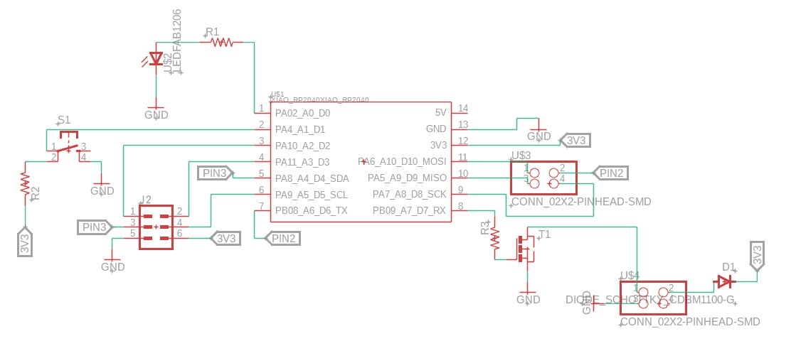
This was my first time designing a PCB. I was excited to create a custom board for the HigiBox project. I used Autodesk Fusion 360 to design both the schematic and the PCB layout. The design included all components integrated directly on the board: an LED indicator, a power button, pull-up resistors, an N-Channel MOSFET for motor control, and a Schottky diode for motor protection.
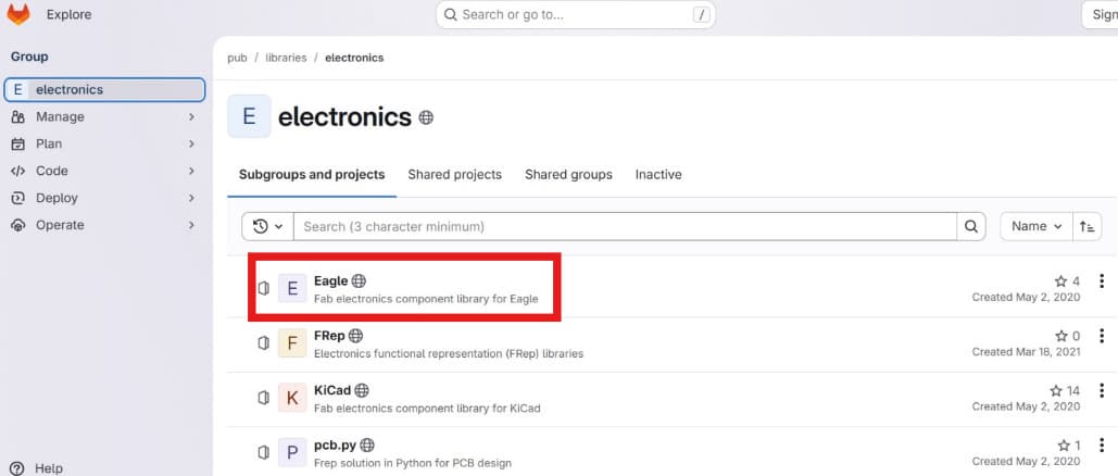
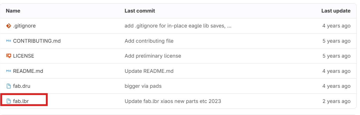
Before starting, I downloaded the Fab Academy component library: gitlab.fabcloud.org/pub/libraries/electronics
📐 Schematic Design
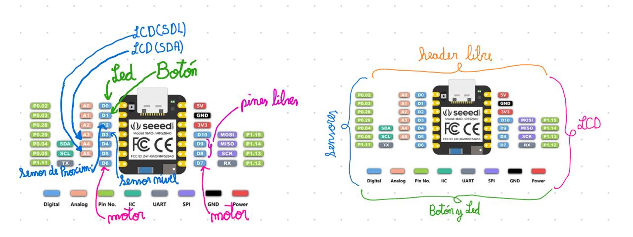
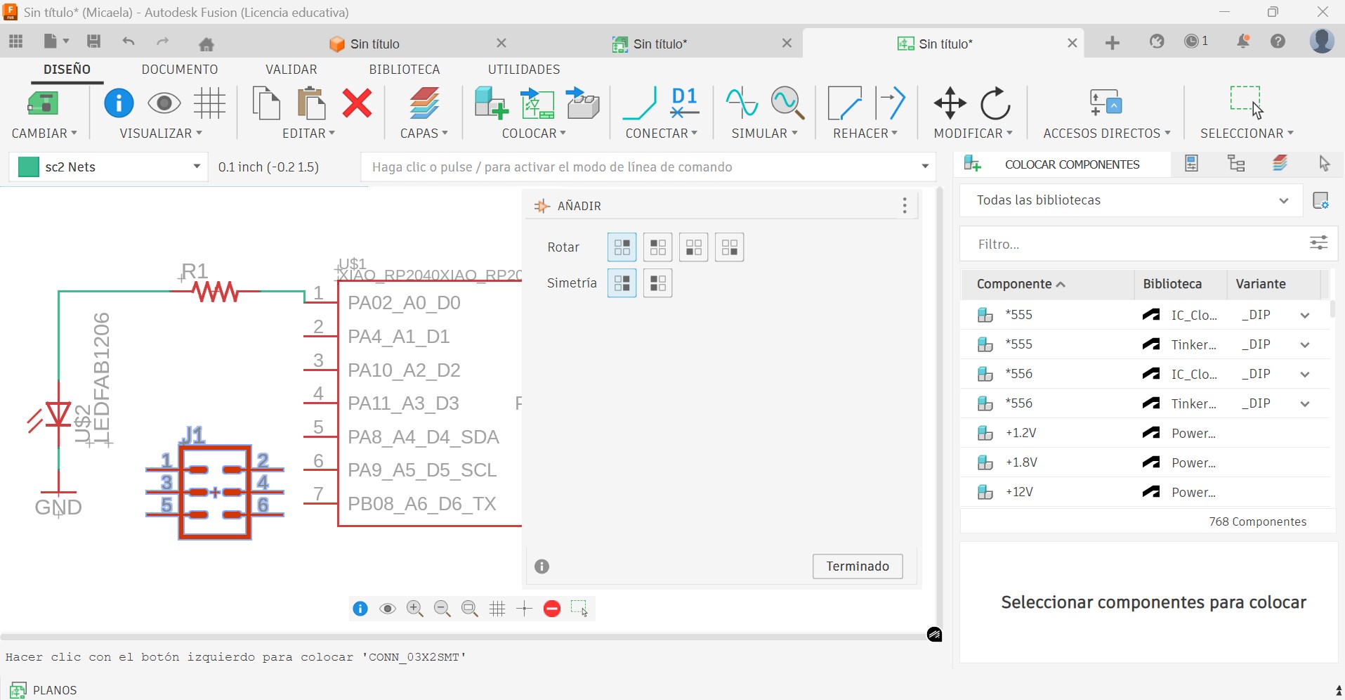
My schematic included: GPIO connections, power distribution, sensor connector header, and motor control circuit with MOSFET and flyback diode.
🖥️ PCB Layout — Where It Failed
After placing all components and routing the traces, I ran the Design Rules Check (DRC) in Fusion 360 to validate that the design was manufacturable.
PCB Layout View:
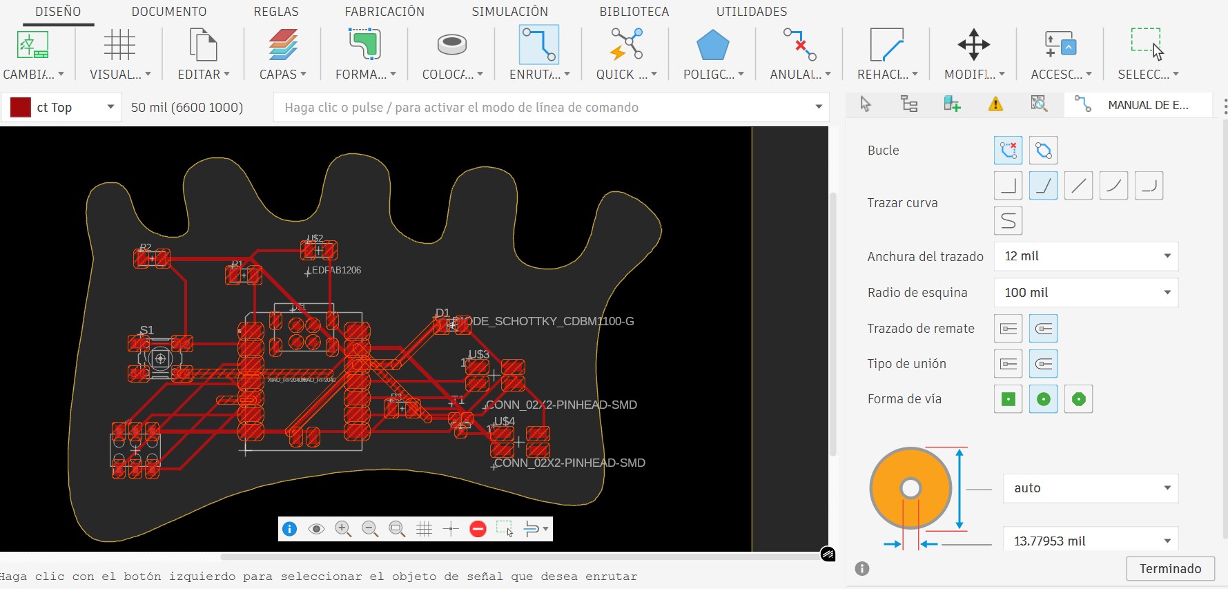
The DRC validation showed 186 errors. My design violated multiple critical electronics design rules:
Multiple copper traces crossed each other without proper layer separation, creating potential short circuits.
Minimum trace-to-trace spacing was violated in many areas, risking unintended electrical connections.
I integrated 15+ components directly on the PCB, creating a dense, difficult-to-route design.
Pads were not optimized for reliable hand-soldering, making assembly risky.
"Regarding your schematic design, you mention that you placed a MOSFET because you want to control a motor. If you want to control the speed and direction of the motor, you should use an H-bridge, but we will cover that in the output devices week. Regarding the PCB layout, the DRC indicates that there are errors — that is because your traces are crossing each other, generating short circuits and undesirable results. You must redo this part of your assignment."
📸 Design Rules Validation Result
The DRC report showed the extent of the failures:
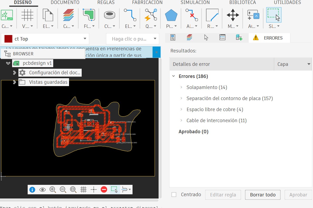
• Solapamiento (Overlap): 14 errors
• Separación del contorno de placa (Board outline separation): 157 errors
• Espacio libre de cobre (Copper clearance): 4 errors
• Cable de interconexión (Trace connection): 11 errors
Total: 186 errors
Design Rule Check is not optional. A design that looks correct electrically can still fail to manufacture. I learned that:
✓ Never attempt to integrate too many components on a single small PCB
✓ Plan modularization: core MCU circuit on PCB, peripherals via headers
✓ Validate with DRC before sending to fabrication
✓ Study the specific milling tool constraints (V-bit angle, trace width limits)
✓ Leave adequate clearance for safe copper routing
This design was not fabricated. It required a complete redesign that led to PCB Version 2 in Week 8.
📋 PCB Design Rules — Critical Principles
During this project, I learned that Design Rule Checks (DRC) are non-negotiable. Here are the 7 fundamental PCB design rules that ensure manufacturability:
- Track Width — Power traces (VCC, GND) must be wider than signal traces to prevent overheating and voltage drops. In our case: GND & 3.3V at 20 mil, signal traces at 12 mil.
- Trace Clearance — Minimum distance between traces to prevent short circuits. The V-bit milling process requires adequate spacing, especially between close parallel traces.
- Drill Size — Holes must be slightly bigger than component pins for easier assembly and reliable connection. SMD pads must be properly sized for hand-soldering.
- Pad Size — Large enough for clean soldering; larger openings reduce hand-soldering errors. Too small = cold joints; too large = waste of PCB real estate.
- Via Size — Well-defined diameter and annular ring for reliable inter-layer connections. In Fab Academy projects with single-sided PCBs, vias are less critical but still important for complex designs.
- Ground Plane — Improves stability, reduces EMI (electromagnetic interference), and provides better current return paths. A solid GND plane is ideal for mixed-signal circuits.
- Trace Length — Long traces can affect signal integrity in high-speed circuits. For embedded systems like HigiBox, this is less critical, but good practice dictates keeping signal traces as short as possible.
PCB Redesign Strategy
During Week 6, I designed my first PCB — but it wasn't good enough. For the Week 8 assignment, I decided to completely redesign the board from scratch. In the first version, I made the critical mistake of integrating 15+ components directly on the PCB. After analyzing the failed design and feedback from my instructor, I realized that several of these components could instead be connected using available free pins through header connectors.
Including everything on the board was unnecessary, created a cramped layout, and caused copper traces to cross each other — which could lead to short circuits and fabrication failures during the milling process.
→ Go to Week 8: Electronics ProductionBefore & After Comparison
15+ integrated components
Traces crossing (shorts)
Dense, unroutable layout
Not fabricated
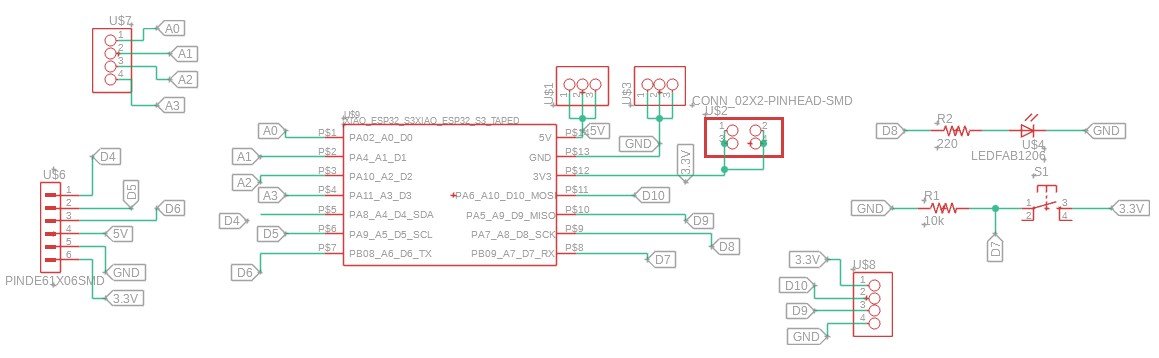
Simplified core circuit
Clean trace routing
Modular header design
Successfully fabricated
🔧 Creating SMD Components in Fusion 360
A critical part of the redesign was creating custom SMD header connectors. The same four-step procedure was followed to create the pin connectors: 1×3, 1×4, and 1×6. Here's the detailed process:
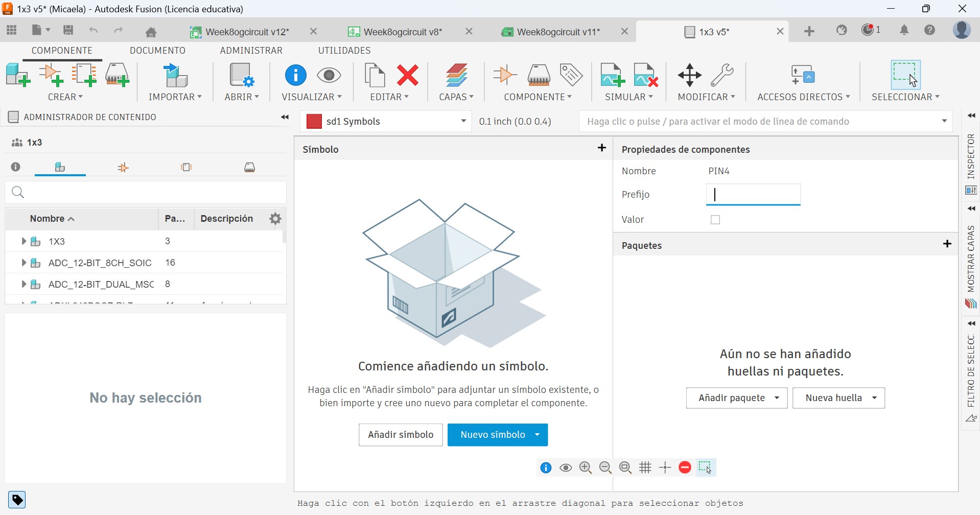
1 Configure Component Properties
The component editor opens in Fusion 360. On the right panel, fill in the Name field (e.g., "CONN_1X3_SMD") and Prefix field (e.g., "J1" for the first connector). Click Añadir símbolo to link an existing symbol from the library, and click Nueva huella to create the PCB footprint.
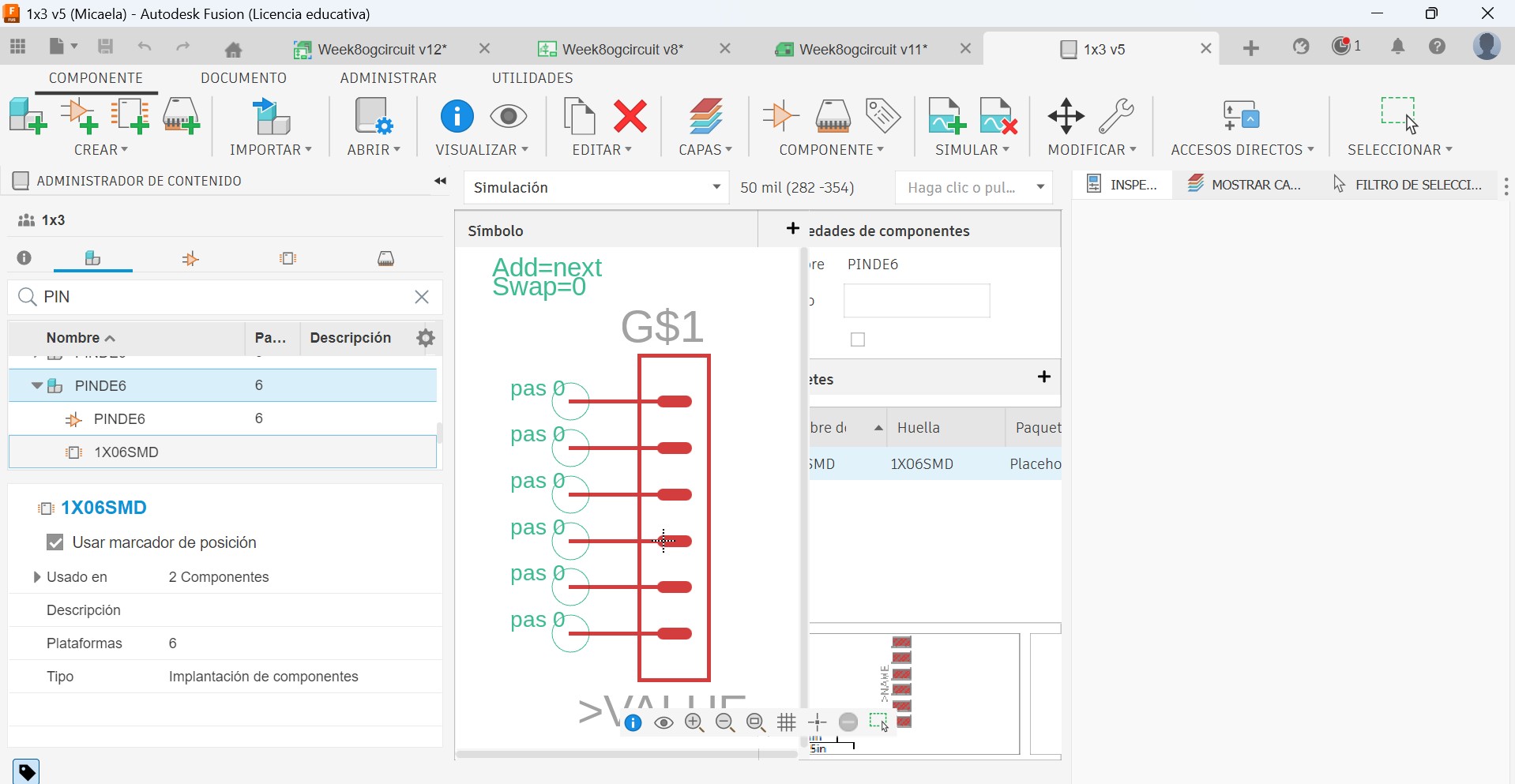
2 Verify Symbol and Associate the Footprint
The left panel in Fusion shows the hierarchical component structure with three levels: component (top level), symbol (schematic representation), and footprint (PCB layout representation). Each level can be edited separately by clicking on it. Verify that both the symbol and footprint are properly assigned before proceeding.
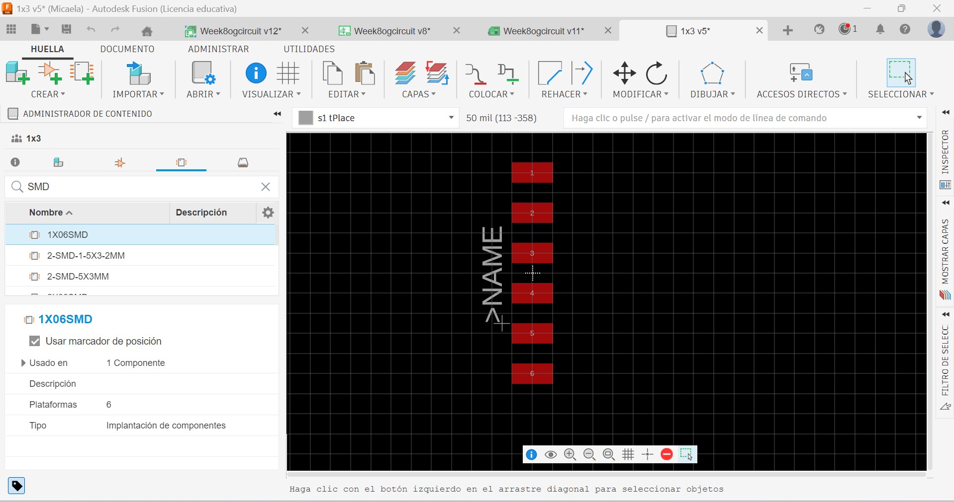
3 Edit the Footprint in the Footprint Editor
Fusion 360 automatically opens the HUELLA (Footprint) tab when you edit the footprint. You can see the SMD pads laid out and numbered 1 to 6 (for a 1×6 connector), vertically aligned on the ct Top copper layer. The pads are rectangular SMD pads optimized for hand-soldering.
4 Link Pins to Pads
A Connect 1X06SMD dialog window opens showing three columns: Pin (from the symbol), Platform (the pad number), and Connection status. Click the Conectar button once for each pin to map logical pins to physical pads. After connecting all pins, click Aceptar to finalize. The component is now ready to use in PCB designs.
PCB Development Across Weeks 8, 15, & 20
📐 Week 8 Design — Electronics Production
After the Week 6 failure, I completely redesigned the PCB for Week 8. This version was simplified, optimized for fabrication, and successfully fabricated using the Roland Modela Pro II MDX-540 CNC milling machine.
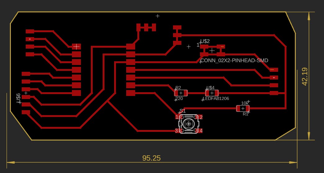
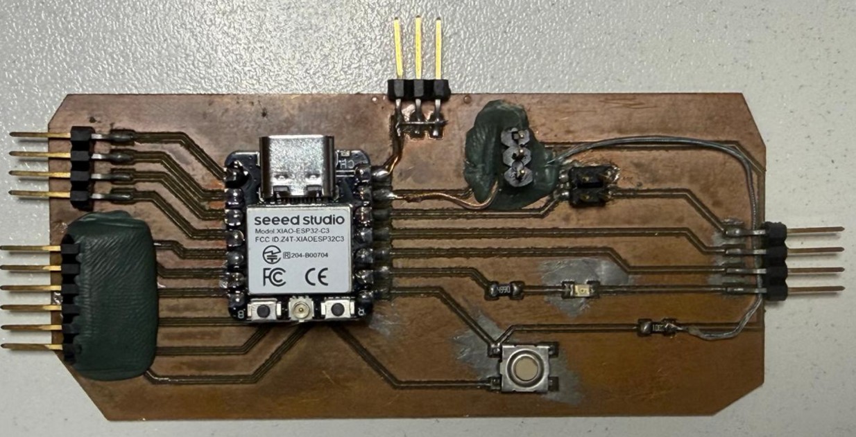
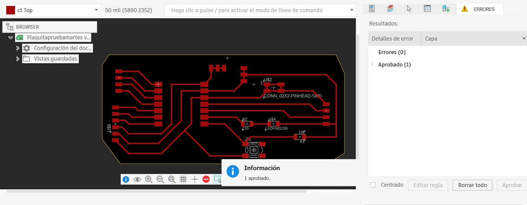
Week 8 PCB Journey: Schematic → Traces → Fabricated Board → Design Rules ✅ Passed
📐 Week 15 Design — PCB Refinement
By Week 15, I had identified additional improvements needed for system integration. The third PCB version was designed with more header outputs, better organization, and full pin management for all HigiBox subsystems.
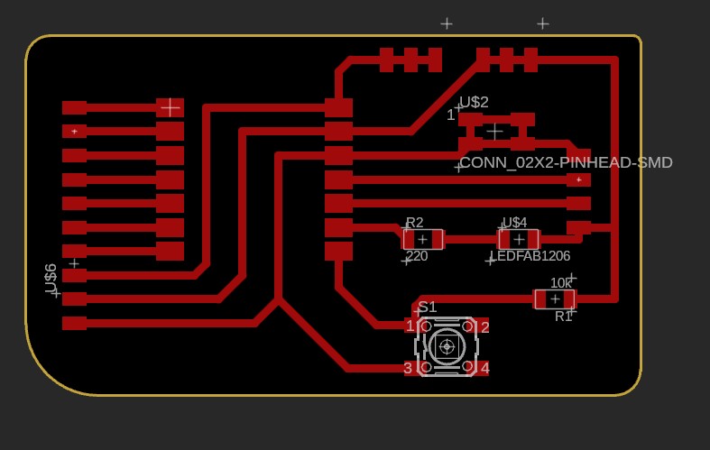
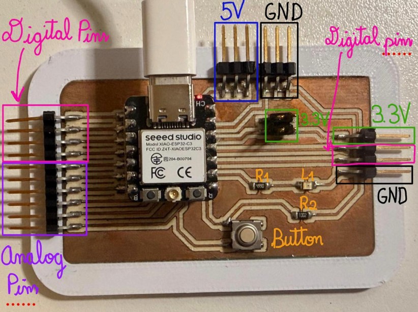
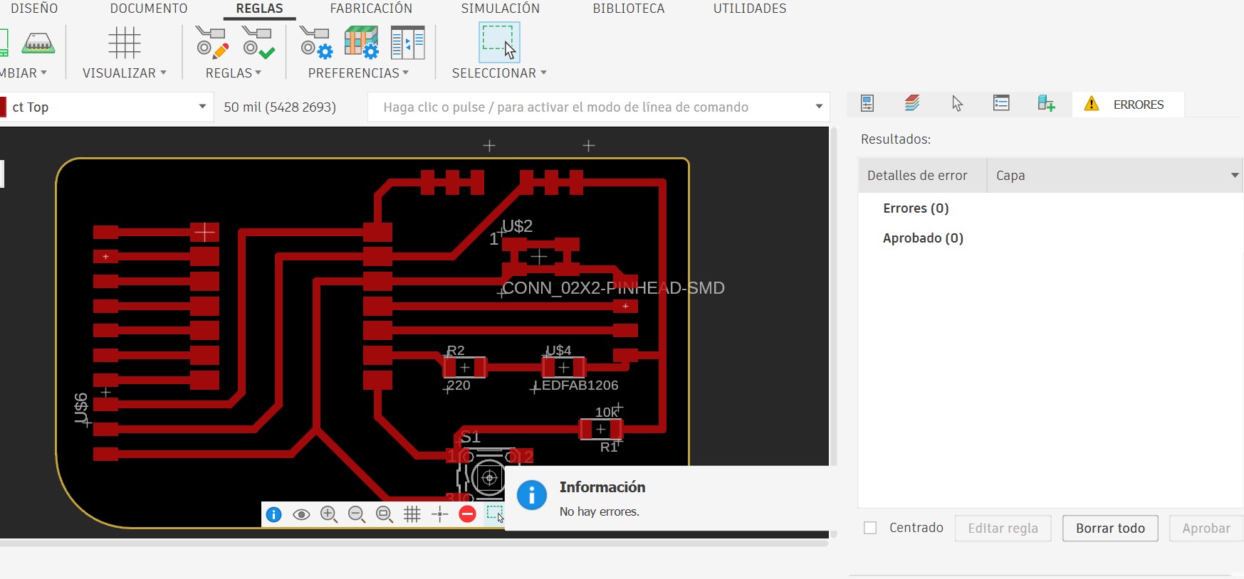
Week 15 PCB Journey: Enhanced Schematic → Improved Routing → Final Integration → Design Rules ✅ Passed
📐 Week 20 Design — HigiBox Final PCB
The final PCB design for HigiBox integrated all lessons learned from previous iterations. This version connected every subsystem seamlessly: sensors, motors, display, power management, and microcontroller, all working in perfect harmony.
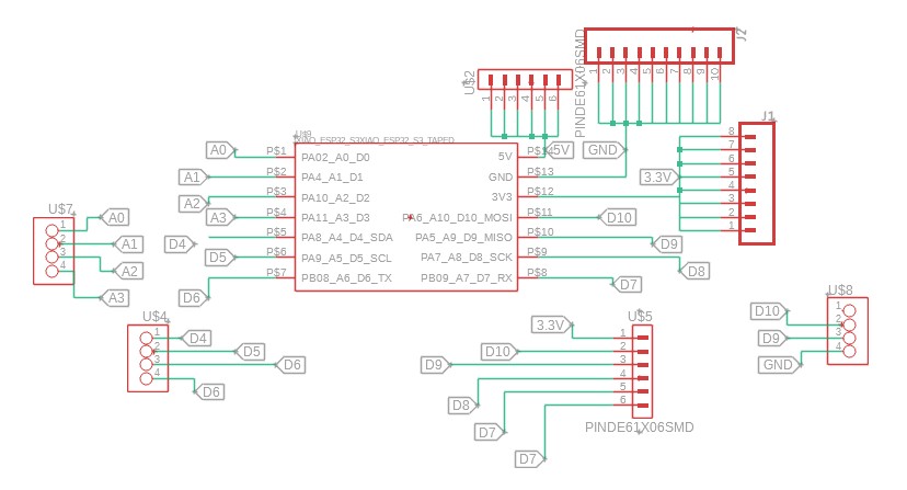
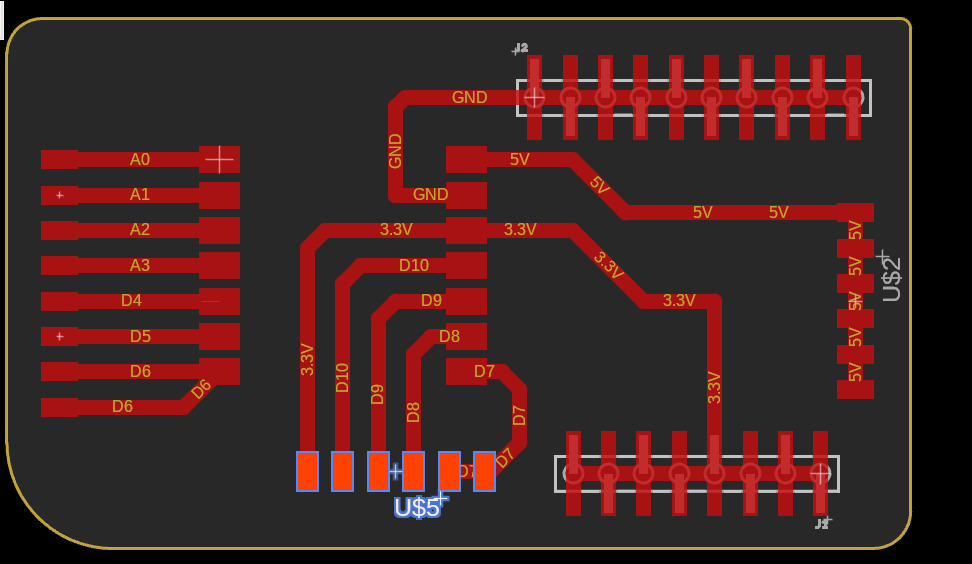
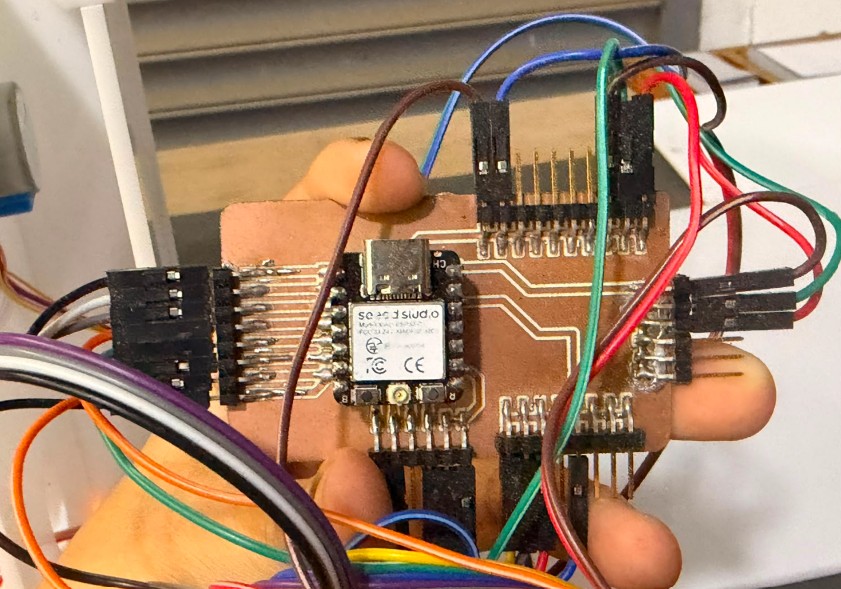
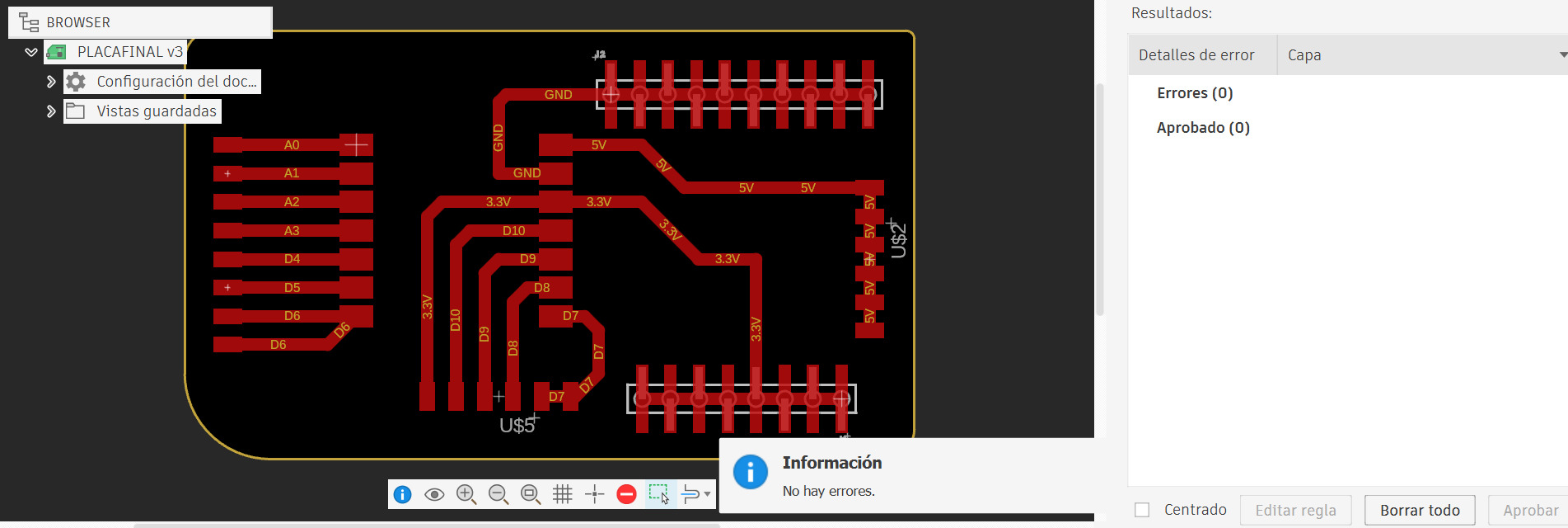
Week 20 Final PCB: Complete Schematic → Final Traces → Manufacturing Ready → Design Rules ✅ Perfect
Week 6: ❌ 186 DRC errors — design failed
Week 8: ✅ Redesigned, fabricated, and tested
Week 15: ✅ Refined with better integration
Week 20: ✅ Final version deployed in HigiBox
Lesson: PCB design is iterative. Each failure teaches you something. The key is to validate early with DRC, simplify aggressively, and modularize through headers.