
What is Embedded Programming?
Embedded programming is the process of developing software that directly controls physical hardware, especially microcontrollers. An embedded system consists of three main components:
Capture information from the environment (temperature, light, pressure, motion)
Processes sensor data and makes decisions based on program logic
Execute actions controlled by the microcontroller (motors, LEDs, buzzers)
What are Microcontrollers?
A microcontroller is a complete system on a single chip. It includes:
- Flash Memory — stores your program permanently
- RAM — temporary memory during execution
- EEPROM — permanent data storage that survives power cycles
- Peripherals — ADC, Timers, GPIO, UART, I2C, SPI, and more
Microcontrollers only understand binary. We write code in C, C++, or MicroPython, and the compiler translates it to machine code that the microcontroller executes.
Development Board Comparison & Analysis
For the group assignment, I worked hands-on with multiple development boards in the Fab Lab, comparing their performance characteristics, ease of use, and suitability for embedded programming. I tested datasheets, investigated microcontroller specifications, and evaluated which boards best suit different application scenarios. The group assignment focused on understanding the toolchains available for different embedded architectures and their practical implications.
Our instructor gave us a quick lesson on reading microcontroller datasheets using the Raspberry Pi Pico 2W as an example. We learned how to interpret pinout diagrams, identify pin functions, and understand the specifications of different development boards.
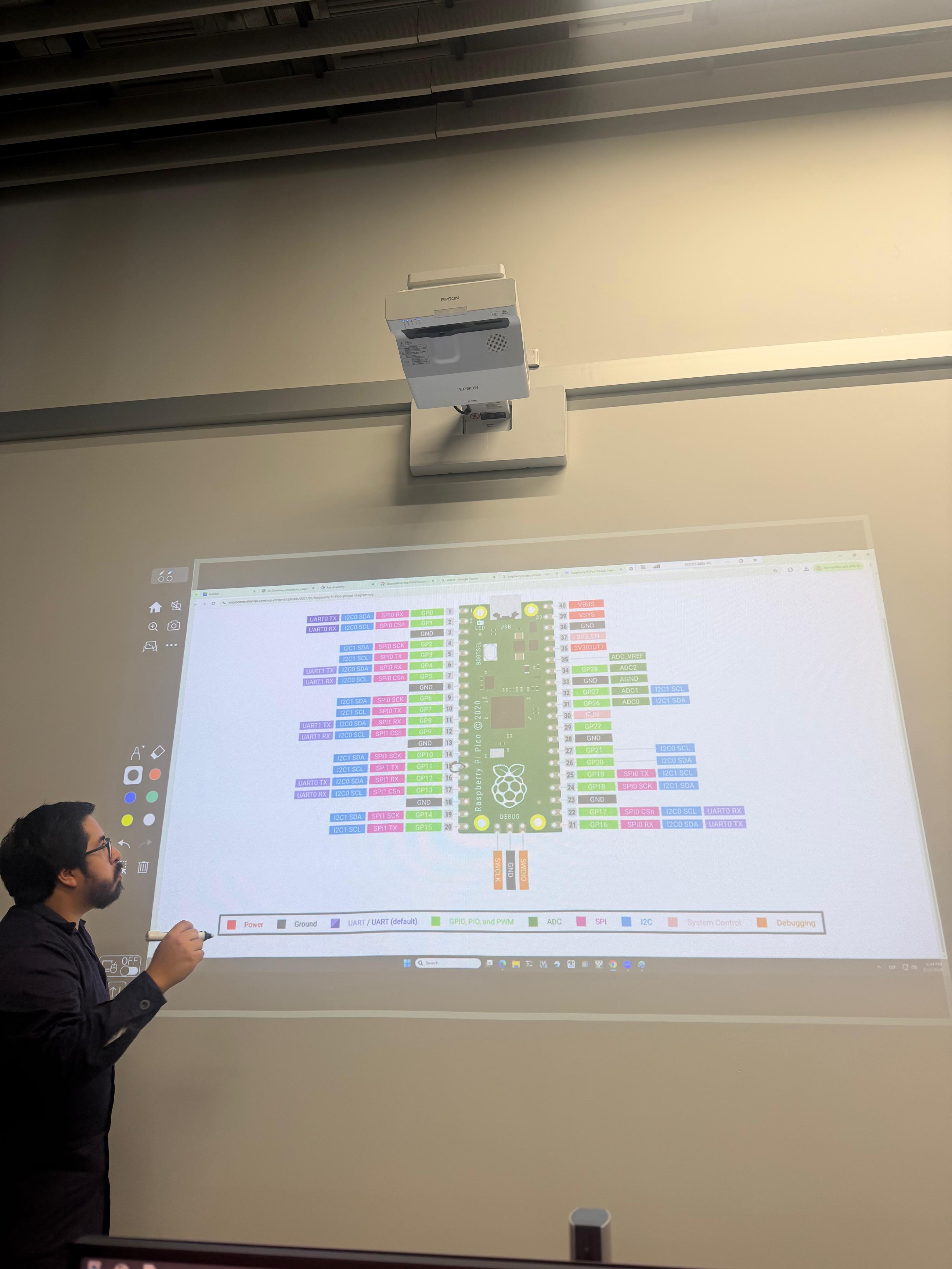
A datasheet is the "contract" between a chip manufacturer and the engineer using it. It specifies:
- Pinout Diagram — which pin does what
- Electrical Characteristics — voltage, current, timing specs
- Memory Map — where code and data go
- Peripheral Descriptions — how to use ADC, timers, communication protocols
- Absolute Maximum Ratings — don't exceed these or you destroy the chip
We tested and documented six different development boards to understand their strengths, weaknesses, and ideal applications. Each represents a different category of embedded systems design.
Board 1: Raspberry Pi Pico 2 W
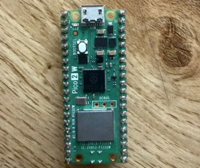
Raspberry Pi Pico 2W
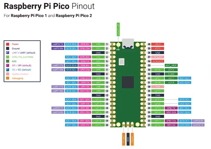
Pinout Diagram
The Raspberry Pi Pico 2 W is a development board with integrated WiFi, allowing use in IoT projects. It operates at 3.3V and includes a voltage regulator that steps down 5V USB power. Its GPIO pins can be configured as digital inputs or outputs. It supports SPI, I2C, and UART communication protocols and features integrated WiFi and Bluetooth Low Energy connectivity.
| Feature | Specification |
|---|---|
| Main MCU | RP2350 (ARM Cortex-M33 dual-core) |
| Clock Speed | Up to 150 MHz |
| Flash / RAM | 4 MB Flash / 520 KB SRAM |
| Digital GPIO | Up to 30 programmable pins |
| ADC | 12-bit (3 channels) |
| Wireless | WiFi + Bluetooth (CYW43439) |
Board 2: Arduino UNO R4 WiFi
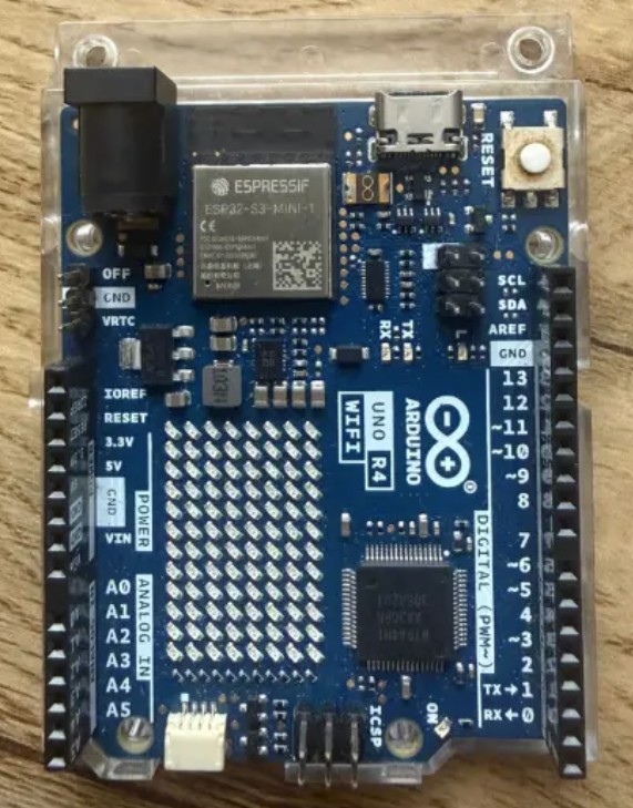
Arduino UNO R4 WiFi
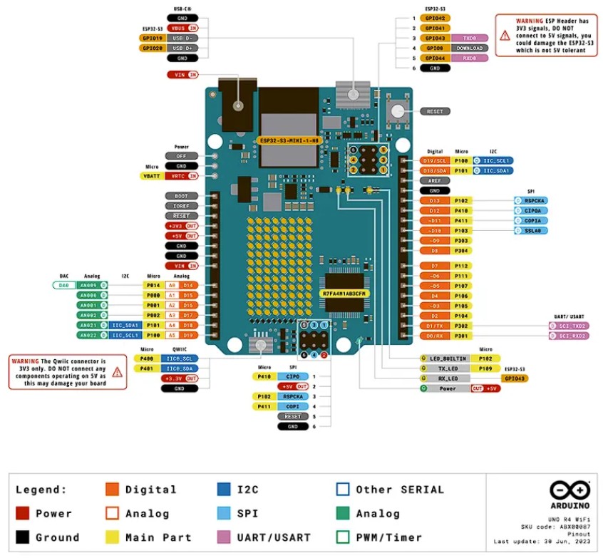
Pinout Diagram
The Arduino UNO R4 WiFi is an upgraded version of the classic UNO platform. It integrates a powerful 32-bit ARM Cortex-M4 microcontroller and an ESP32-S3 WiFi/Bluetooth module. It operates at 5V logic level for backward compatibility with Arduino shields and provides extensive connectivity options for IoT applications.
| Feature | Specification |
|---|---|
| Main MCU | R7FA4M1AB3CFM#AA0 (ARM Cortex-M4) |
| Flash / SRAM | 256 kB Flash / 32 kB SRAM |
| Digital Pins | 14 |
| ADC | 14-bit |
| Wireless | WiFi + BLE 5 (via ESP32-S3) |
| Special | CAN Bus, DAC (12-bit) |
Board 3: Arduino UNO R3
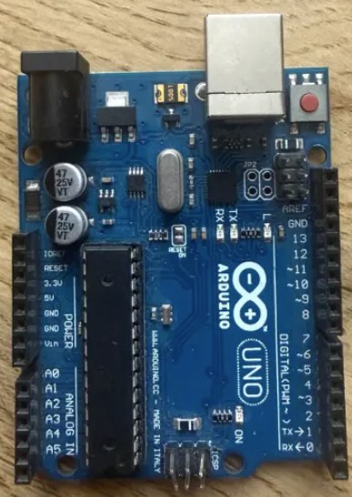
Arduino UNO R3
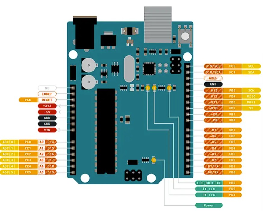
Pinout Diagram
The Arduino UNO R3 is one of the most popular development boards for learning embedded systems. It uses the ATmega328P 8-bit AVR microcontroller and is widely used in education and beginner projects. It provides a simple and accessible way to understand how hardware and software interact.
| Feature | Specification |
|---|---|
| Main MCU | ATmega328P (8-bit AVR) |
| Clock Speed | 16 MHz |
| Flash / SRAM | 32 kB Flash / 2 kB SRAM |
| Digital Pins | 14 |
| Analog Inputs | 6 |
| PWM | 6 channels |
Board 4: Seeeduino XIAO nRF52840
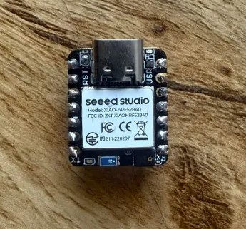
Seeeduino XIAO nRF52840
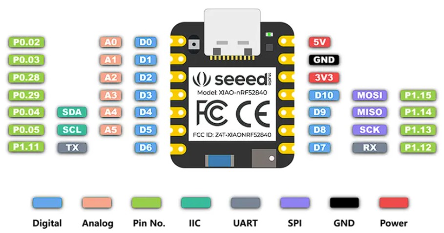
Pinout Diagram
The Seeeduino XIAO nRF52840 is a compact and powerful development board optimized for IoT and Bluetooth applications. Despite its small size, it integrates wireless communication and advanced low-power features, making it ideal for wearables and battery-powered devices.
| Feature | Specification |
|---|---|
| Main MCU | nRF52840 (ARM Cortex-M4F) |
| Flash / RAM | 1 MB Flash / 256 kB RAM |
| Clock Speed | 64 MHz |
| Digital Pins | Up to 14 |
| Bluetooth | BLE 5.0 |
| ADC | 12-bit |
Board 5: ESP32 (ESP32-WROOM)
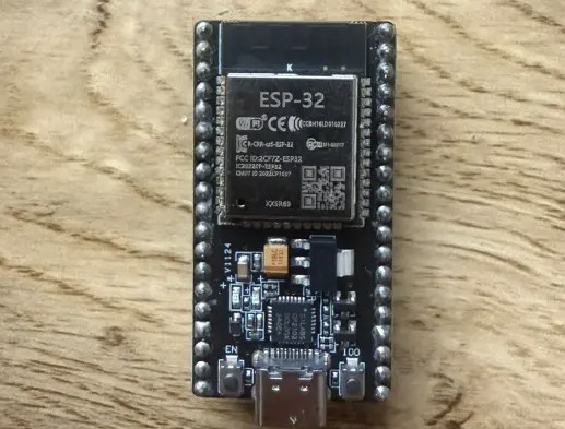
ESP32 Board
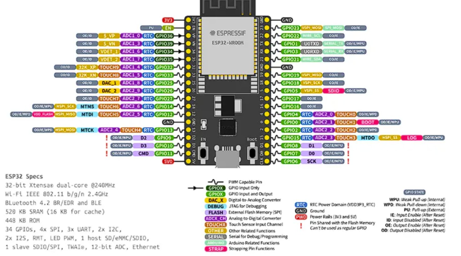
Pinout Diagram
The ESP32 development board is designed for IoT and wireless applications with a powerful dual-core processor and built-in WiFi and Bluetooth. It operates at 3.3V logic level and is widely used for smart devices, home automation, and wireless control systems. It offers significantly higher processing speed and memory than traditional Arduino boards.
| Feature | Specification |
|---|---|
| Main MCU | Xtensa LX6 (dual-core) |
| Clock Speed | Up to 240 MHz |
| Flash / RAM | ~4 MB Flash / 520 kB SRAM |
| Digital GPIO | Up to 34 pins |
| Wireless | WiFi + Bluetooth Classic + BLE |
| ADC / DAC | 12-bit ADC / 2×8-bit DAC |
Board 6: Arduino Nano
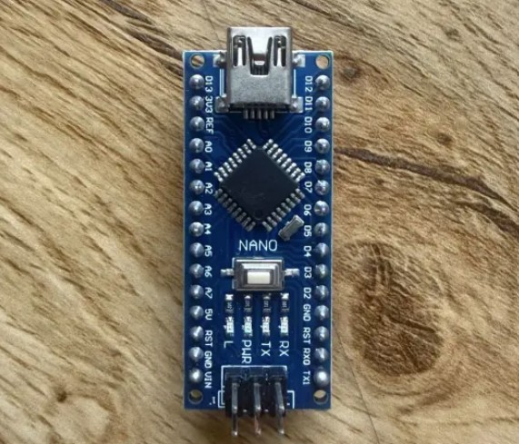
Arduino Nano
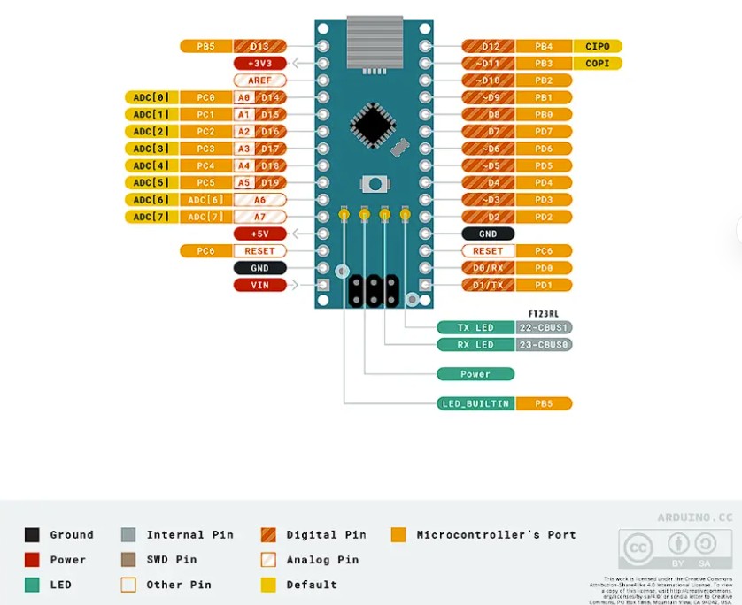
Pinout Diagram
The Arduino Nano offers similar functionality to the UNO but in a much smaller form factor. It uses the same ATmega328P microcontroller and is commonly used in compact or space-limited projects such as wearable devices or small embedded prototypes while maintaining the same programming experience.
| Feature | Specification |
|---|---|
| Main MCU | ATmega328P (8-bit AVR) |
| Clock Speed | 16 MHz |
| Flash / SRAM | 32 kB Flash / 2 kB SRAM |
| Digital Pins | 14 |
| Analog Inputs | 8 |
| Form Factor | Compact, breadboard-friendly |
Side-by-side comparison of all six boards to help identify which is best for different applications:
| Feature | UNO R3 | Nano | UNO R4 | ESP32 | Pico 2 W | XIAO |
|---|---|---|---|---|---|---|
| Architecture | 8-bit AVR | 8-bit AVR | 32-bit Cortex-M4 | 32-bit Xtensa (dual) | 32-bit Cortex-M33 (dual) | 32-bit Cortex-M4F |
| Clock Speed | 16 MHz | 16 MHz | 48 MHz | Up to 240 MHz | Up to 150 MHz | 64 MHz |
| Flash | 32 kB | 32 kB | 256 kB | ~4 MB | 4 MB | 1 MB |
| RAM | 2 kB | 2 kB | 32 kB | 520 kB | 520 kB | 256 kB |
| Digital Pins | 14 | 14 | 14 | Up to 34 | Up to 30 | Up to 14 |
| WiFi | No | No | Yes (2.4 GHz) | Yes (2.4 GHz) | Yes (2.4 GHz) | No |
| Bluetooth | No | No | BLE 5 | Classic + BLE | BLE 5.2 | BLE 5.0 |
| Best For | Education basics | Compact projects | IoT intermediate | IoT advanced | WiFi connected | Wearables |
ESP32 Setup with Arduino IDE
Setting up the ESP32 with Arduino IDE requires several steps: installing the USB driver, configuring the IDE, and selecting the correct board and port.
Connect the ESP32 to your computer. If Device Manager shows a yellow warning, download and install the CP2102 driver from Silicon Labs.

Download from arduino.cc/en/software
File → Preferences → Add this URL to "Additional boards manager URLs":
Tools → Board → Boards Manager → Search "esp32" and install "esp32 by Espressif Systems"
Tools → Board → "ESP32 Dev Module"
Tools → Port → Select your COM port
ESP32 — Complete Technical Investigation
This section is a comprehensive technical deep-dive into the ESP32 microcontroller, the heart of my HigiBox project. I chose to investigate one platform in depth rather than compare many, to truly understand its capabilities, limitations, and internal workings.
The ESP32 is a system-on-chip (SoC) that integrates a powerful processor, memory, wireless radios, and extensive peripherals in a single chip. For HigiBox, it is ideal because:
Simultaneous WiFi/BT communication and dispenser control without blocking. Core 0 handles wireless; Core 1 manages real-time motor/sensor logic.
WiFi 802.11 b/g/n (2.4 GHz) + Bluetooth Classic + BLE. No separate modules needed. Reduces PCB footprint and cost.
16 PWM channels, 12-bit ADC, I2C, SPI, UART, touch sensors, timers. Covers all HigiBox requirements without external glue logic.
Development boards under $10. Production modules under $5. Ideal for consumer IoT devices and wearables.
My board uses the ESP32-WROOM-32E, which is the standard production module. Below are the complete specifications:
Processor & Memory
| Parameter | Value | Notes |
|---|---|---|
| CPU | Dual Xtensa 32-bit LX6 | Up to 160 MHz per core, configurable |
| Max Clock Speed | 240 MHz (turbo mode) | Consumes more power; standard is 160 MHz |
| Flash Memory | 4 MB (embedded) | Stores bootloader, app code, and calibration data |
| SRAM | 520 KB | Internal RAM for heap, stack, and variables |
| PSRAM (Optional) | Up to 16 MB | External SPI RAM; ESP32-WROVER variant |
| RTC Memory | 8 KB | Survives deep sleep; useful for persistent state |
| I-Cache | 32 KB | Instruction cache per core |
| D-Cache | 32 KB | Data cache per core |
Power & Operating Conditions
| Parameter | Min | Typical | Max |
|---|---|---|---|
| Operating Voltage | 2.3 V | 3.3 V | 3.6 V |
| Current — Idle | — | 10 mA | — |
| Current — WiFi TX | — | 160 mA | 240 mA |
| Current — Deep Sleep | — | 10 µA | 150 µA |
| Temp. Range | -40 °C | — | 85 °C |
GPIO Pins (34 total available)
The ESP32 has 34 GPIO pins, but not all are equally suitable for every application. Some pins are reserved, strapping pins affect boot mode, and some have limited functionality:
GPIO34, GPIO35, GPIO36, GPIO39 — Can only be used as inputs (no output capability). Ideal for analog sensors or button inputs since they don't drive loads.
GPIO0, GPIO2, GPIO5, GPIO12, GPIO15 — Affect boot mode during startup. Pulling them to wrong levels can prevent the board from booting. Use with caution or avoid for application logic.
Peripheral Inventory
| Peripheral | Count/Type | HigiBox Usage |
|---|---|---|
| PWM (LED) | 16 channels @ 1–8 bits | Control motor speed (1 channel) |
| ADC | 2× 12-bit SAR ADC; ADC1 (8 ch), ADC2 (10 ch) | Stock sensor on ADC1 (ADC2 conflicts with WiFi) |
| DAC | 2× 8-bit | Not used; could drive analog circuit |
| I2C | 2× (I2C0, I2C1) | OLED display connection |
| SPI | 3× (HSPI, VSPI, SPI3) | Optional SD card logging |
| UART | 3× (UART0, UART1, UART2) | UART0 for programming; UART1 for external sensors |
| Timers | 4× 64-bit timers | Motor pulse timing, event scheduling |
| Touch Sensors | 10 capacitive touch channels | Alternative to mechanical buttons |
| CAN (TWAI) | 1× CAN 2.0B | Not used; industrial applications |
| RMT | 8 channels | Optional: WS2812 RGB LED addressable control |
WiFi (802.11 b/g/n @ 2.4 GHz)
- Standards: 802.11 b (1, 2, 5.5, 11 Mbps) / g (6–54 Mbps) / n (up to 150 Mbps)
- Modes: Station (STA), SoftAP (AP), Station+AP (concurrent)
- Security: WEP, WPA, WPA2, WPA3 support
- Typical Current: RX 80 mA, TX 160–240 mA (varies by power level)
- Issue: Blocks ADC2 when active; cannot use ADC2 while WiFi transmitting
Bluetooth & BLE (2.4 GHz)
- Classic Bluetooth: 2.1 with EDR (Enhanced Data Rate)
- BLE: Bluetooth 4.2 compliant
- Concurrent: WiFi + BT or WiFi + BLE simultaneously
- BLE Current Draw: ~5–15 mA RX, ~15–30 mA TX (much lower than WiFi)
- Ideal for HigiBox: BLE is preferred for mobile app (lower power, ideal for IoT)
RF Front-End
- Antenna: Printed PCB antenna or external antenna connector on some modules
- Transmit Power: Up to +20 dBm (100 mW) in standard mode
- Receiver Sensitivity: Typical -95 dBm @ 11 Mbps (WiFi), -92 dBm @ 1 Mbps (BLE)
- Range: Typically 30–50 meters indoors, up to 100 meters in optimal conditions
Espressif produces multiple ESP32 variants. Understanding the differences is critical for production design:
| Variant | Flash | PSRAM | Size | Best For |
|---|---|---|---|---|
| WROOM-32E | 4 MB | No | 18×25.5 mm | Standard IoT (my choice) |
| WROVER | 4 MB | 8 MB | 18×31.4 mm | Apps needing large buffers |
| WROOM-32U | 4 MB | No | 18×25.5 mm | Industrial, extended temp range |
| SOLO (ESP8266-like) | 2/4 MB | — | Smaller | WiFi only, cost-critical |
| MINI | 4 MB | No | 13×17 mm | Compact wearables (HigiBox v2?) |
Boot Sequence (Power-On Reset)
- ROM Bootloader (Mask ROM): Always runs first, 128 KB fixed code burned at manufacturing. Checks strapping pins to determine boot mode.
- Strapping Pins Decision:
- GPIO0=0, GPIO2=0 → Download mode (firmware upload from UART)
- GPIO0=1 → Normal boot from flash
- Second-Stage Bootloader: Loads from flash address 0x1000. Initializes flash, loads partition table, verifies digital signatures if enabled.
- Partition Table: Defines flash layout (bootloader, partitions, NVS storage, SPIFFS filesystem if used)
- Application Load: bootloader copies your firmware from flash into RAM and jumps to entry point
- User Setup(): Your setup() function runs; WiFi stack initializes if enabled
- loop(): Main program execution begins
Sleep Modes & Power States
| Mode | Current Draw | Wake Time | Use Case |
|---|---|---|---|
| Active (Normal) | 60–160 mA | — | Running application, WiFi/BLE active |
| Modem Sleep | 20 mA | Instant | CPU running, WiFi/BT off (useful for quick tasks) |
| Light Sleep | 0.8–10 mA | ~6 ms | CPU paused, timers/ADC running, can wake on GPIO interrupt |
| Deep Sleep | 10–150 µA | ~1 second | Only RTC logic alive, ULP coprocessor, external trigger or timer |
| Hibernation | 2.5 µA | ~5 seconds | Extreme power saving; minimal wake capability |
ESP32 Internal Architecture — Block Diagram Mapping
• Core 0: Runs WiFi/BT stack in real-time.
• Core 1: Runs user application logic.
• Shared L1 caches (32 KB I-cache, 32 KB D-cache per core).
• Independent operation allows simultaneous connectivity + control.
Survives deep sleep. Manages wake scheduling, clock calibration, low-power sensor monitoring.
Hardware acceleration for cryptographic operations. Protects OTA firmware updates, TLS/SSL handshakes, and secure WiFi (WPA3).
One-time programmable eFuses store MAC address, calibration data, flash encryption keys, secure boot keys. Enables secure OTA and tamper protection.
ADC2 becomes unavailable when WiFi transmits. For HigiBox stock sensor (weight or optical), connect to ADC1 pins (GPIO32–39). No conflicts with wireless operation.
16 PWM channels available. Use one for motor control. Frequency 5 Hz–40 kHz allows precise pulse width modulation (e.g., 100ms motor pulse = 1 pill).
Core 0 handles WiFi/BLE stack automatically. Core 1 runs your dispenser logic without blocking on wireless events. No need for async event handling complexity.
Between dispensing events, enable deep sleep (10 µA draw). Wake via timer interrupt every 24 hours for BLE advertisement and stock check. A 2000 mAh battery = 8+ months runtime.
Mobile app should use Bluetooth Low Energy (BLE) for control/alerts, not WiFi. WiFi consumes 160 mA; BLE only 5–30 mA. Reserve WiFi for critical cloud logging only.
Partition flash with dual OTA slots. Hardware crypto engine verifies signatures during firmware updates. Prevents downgrade attacks and ensures production reliability.
ADC2 unavailable during active WiFi transmission. This is a hardware limitation of how the SPI bus is shared. Plan sensor connections for ADC1.
GPIO0, GPIO2, GPIO5, GPIO12, GPIO15 affect boot mode. Avoid using them as application GPIO if possible. If necessary, document pull-up/pull-down requirements carefully.
PCB antenna is direction-dependent and sensitive to component placement. Poor antenna design reduces range from 100m to 5m. If range is critical, use external antenna option (WROVER modules).
No hardware FPU. Floating-point math is slow (emulated in software). For time-critical code, prefer integer math. This is rarely a problem for IoT devices.
Each GPIO pin can source/sink ~20 mA maximum. For high-current devices (motors, heaters), use external MOSFETs or relay drivers. N20 motor draws ~100 mA — use a driver circuit.
Internal voltage regulators are sensitive to supply noise. Use low-ESR capacitors (0.1 µF + 10 µF) close to ESP32 power pins. Poor filtering causes WiFi instability.
Cryptographic Accelerators (Hardware)
- SHA-256/SHA-1: Message digest for firmware verification and TLS handshakes. ~10× faster than software SHA.
- AES-128 (ECB/CBC): Block cipher for flash encryption and secure communication. Hardware accelerated, essential for real-time encrypted streams.
- RSA-4096: Asymmetric cryptography for secure boot and OTA signature verification. Slower but necessary for firmware authenticity.
- Random Number Generator: Hardware TRNG (True RNG) based on RF noise. Critical for generating cryptographic keys and nonces.
Flash Encryption & Secure Boot
- Flash Encryption: Optional hardware-enabled encryption of entire flash contents using AES-128. Transparent to application — data decrypted on-the-fly during execution.
- Secure Boot: Bootloader verifies RSA-4096 signature of application before executing. Prevents unauthorized firmware installation.
- eFuse Keys: Encryption and signing keys stored in one-time-programmable eFuses. Cannot be read back externally — only chip can use them.
TLS/SSL Support
- OpenSSL and mbedTLS libraries included in SDK
- Hardware crypto acceleration for TLS handshakes and encrypted data transfer
- Support for certificate validation and mutual authentication
Why I chose ESP32 over alternatives:
| Chip | CPU | Flash | Wireless | Cost | Best For |
|---|---|---|---|---|---|
| ESP32 (my choice) | Xtensa LX6 dual-core @ 240 MHz | 4 MB | WiFi + BT/BLE | $3–5/chip | IoT with cloud connectivity and mobile app |
| STM32H7 | Cortex-M7 @ 480 MHz | Up to 2 MB | None (require external modules) | $5–10 | High-performance real-time systems, motor control |
| nRF52840 | Cortex-M4F @ 64 MHz | 1 MB | BLE only | $8–12 | Wearables, low-power BLE-only devices |
| Raspberry Pi Pico | Cortex-M0+ dual-core @ 133 MHz | 2 MB | None | $4–5 | Educational, simple embedded projects (no wireless) |
| SAMD21 | Cortex-M0+ @ 48 MHz | 256 KB | None | $2–3 | Arduino-compatible Arduino Zero (very limited resources) |
✓ Needs WiFi + BLE → ESP32 only choice
✓ Battery-powered IoT → ESP32 beats STM32
✗ STM32 faster but requires external WiFi module (cost + complexity)
✗ Raspberry Pi Pico has no wireless
✗ nRF52840 better for BLE-only, but no WiFi
ESP32 is the only chip that does everything HigiBox needs in one package.
All ESP32 technical information is publicly available from Espressif:
| Document | Purpose | Key Info |
|---|---|---|
| ESP32 Datasheet | Hardware specification | Pin assignments, electrical characteristics, timing specs, absolute maximum ratings |
| ESP32 Technical Reference Manual | Internal architecture | Register descriptions, peripheral operation, interrupt handling, memory map (500+ pages) |
| ESP32 Hardware Design Guide | PCB design recommendations | Power supply, decoupling, antenna design, signal integrity, EMC considerations |
| ESP-IDF Programming Guide | Software development framework | APIs for WiFi, BLE, timers, ADC, sleep modes, OTA updates |
| ESP32-WROOM-32E Datasheet | Module-level specs | Pinout, antenna type, power consumption, operating range, compliance certifications |
Setting Up Your First Program
Once your ESP32 is physically set up and the drivers are installed, you're ready to write your first program. Here's a complete workflow for setting up a simple program in Arduino IDE.
File → New opens a blank sketch template. By default, Arduino IDE gives you a skeleton with setup() and loop() functions.
File → Save or use the keyboard shortcut. Arduino will create a folder with your sketch name and save a .ino file inside.
The structure of every Arduino sketch is:
Common initialization tasks in setup():
pinMode(pin, OUTPUT)— declare a pin as output (for LEDs, motors)pinMode(pin, INPUT)— declare a pin as input (for buttons, sensors)Serial.begin(115200)— open serial communication at 115200 baud
Sketch → Verify/Compile or press the Verify button (checkmark icon). The IDE checks for syntax errors and compiles your code. If there are issues, error messages appear in the console below.
Sketch → Upload or press the Upload button (arrow icon). The IDE will:
- Compile your sketch again
- Detect your board and COM port
- Send the compiled code to the ESP32 via USB
- Print status messages as the upload progresses
If your sketch uses Serial.println() to print debug messages, open the Serial Monitor to see them in real time.
Tools → Serial Monitor or press Ctrl+Shift+M
- Make sure the baud rate matches your code (usually 115200)
- You'll see all messages your program sends to Serial
- Useful for debugging and understanding what your program is doing
Button pressed: 1234
LED turned ON
Motor speed: 128 / 255
Board not detected. Check USB cable, reinstall CP2102 driver, and verify the correct port is selected in Tools → Port.
Usually a baud rate mismatch or corrupted upload. Try uploading again. If it persists, hold the "Boot" button on the ESP32 while uploading.
Check the error message in the console. Common issues: missing semicolons, mismatched brackets, undefined variables. The IDE highlights the line with the error.
If it uploads but doesn't do what you expect, open the Serial Monitor to see if there are runtime errors or unexpected behavior in your loop.
Essential Arduino Functions Cheat Sheet
| Function | Purpose | Example |
|---|---|---|
pinMode(pin, mode) |
Set pin as INPUT or OUTPUT | pinMode(2, OUTPUT); |
digitalWrite(pin, value) |
Set pin to HIGH or LOW | digitalWrite(2, HIGH); |
digitalRead(pin) |
Read pin state (HIGH or LOW) | int state = digitalRead(5); |
analogRead(pin) |
Read analog value (0–4095) | int value = analogRead(34); |
analogWrite(pin, value) |
PWM output (0–255) | analogWrite(18, 128); |
delay(ms) |
Pause execution (milliseconds) | delay(1000); |
Serial.begin(baud) |
Start serial communication | Serial.begin(115200); |
Serial.println() |
Print message + newline to Serial | Serial.println("Hello"); |
7 Programming Activities
These activities progress from simple digital output to complex sensor integration and system interactions. Each includes code, downloadable .ino file, and demonstration video.
Blink — LED Flashing
📌 Purpose: Turn the ESP32's built-in LED on and off every second. The "Hello World" of embedded systems.
Explanation: The built-in LED on pin 2 blinks with 1-second intervals (500ms ON + 500ms OFF). Perfect for testing if your board and IDE are set up correctly.
Code:
Key Concepts: pinMode() declares a pin as output, digitalWrite() sets HIGH (on) or LOW (off), delay() pauses in milliseconds.
Button Control — LED On/Off
📌 Purpose: Turn an LED on when a button is pressed, off when released. Introduces INPUT reading and conditional logic.
Code:
Key Concepts: INPUT_PULLUP uses the internal pull-up resistor. digitalRead() reads the button state. The "!" operator inverts the logic.
Blinking Control — Fixed 1-Second Cycle
📌 Purpose: Blink an LED with precise 1-second intervals (500ms ON + 500ms OFF).
Code:
Light Sensor (LDR) — Auto Night Light
📌 Purpose: Read an analog light sensor and automatically turn on an LED when it gets dark. Introduces ADC (analog-to-digital conversion).
Code:
Potentiometer Control — LED Brightness
📌 Purpose: Use a potentiometer to control LED brightness. Combines analog input with PWM (Pulse Width Modulation) output.
Code:
Temperature Sensor (LM35) — Color Alert
📌 Purpose: Monitor temperature with an LM35 sensor and change LED color when threshold is exceeded.
Code:
LED Sequence — Chase Animation
📌 Purpose: Create a visually appealing LED sequence that goes UP (1→5) then DOWN (5→1). Demonstrates arrays and loops.
Code:
📥 Download Resources
📥 Download All Activity Files (.ino)
📊 Datasheets & Documentation
Get in Touch
- micaela.cordova.carmelino@gmail.com
- ml.cordovac@alum.up.edu.pe