// Week 08
Electronics Production
Introduction
This week focuses on the physical production of circuit boards. I designed, milled, and assembled a custom microcontroller development board based on the Seeed Studio XIAO RP2040. The goal was to understand the full workflow from digital EDA (Electronic Design Automation) to a functional, "stuffed," and programmed hardware device.
Objectives
Group Assignment
- Characterize the design rules for our in-house PCB production process.
- Document settings for the milling machine (speeds, feeds, tooling).
- Document the workflow for sending a PCB to a boardhouse.
Group Assignment documentation →
Individual Assignment
- Make and test a microcontroller development board.
- Demonstrate tool-path generation, milling, soldering (stuffing), and programming.
- Identify problems and implement fixes during the fabrication process.
Tools & Technologies
1. KiCad 9.0 (EDA)
I used KiCad for schematic design, PCB routing, and generating output files required for toolpath generation.
2. Desktop CNC Router (PCB Milling Machine)
Equipped with a high-speed spindle to mill isolation traces in copper stock and cut the final board outline.
3. Tooling
- 0.1mm 30° V-bit: Used for trace isolation engraving.
- 1.0mm Flat End Mill: Used for cutting board outlines (Edge Cuts).
Process & Workflow
INDIVIDUAL PROJECT: CUSTOM XIAO RP2040 SHIELD
Design & Board Preparation
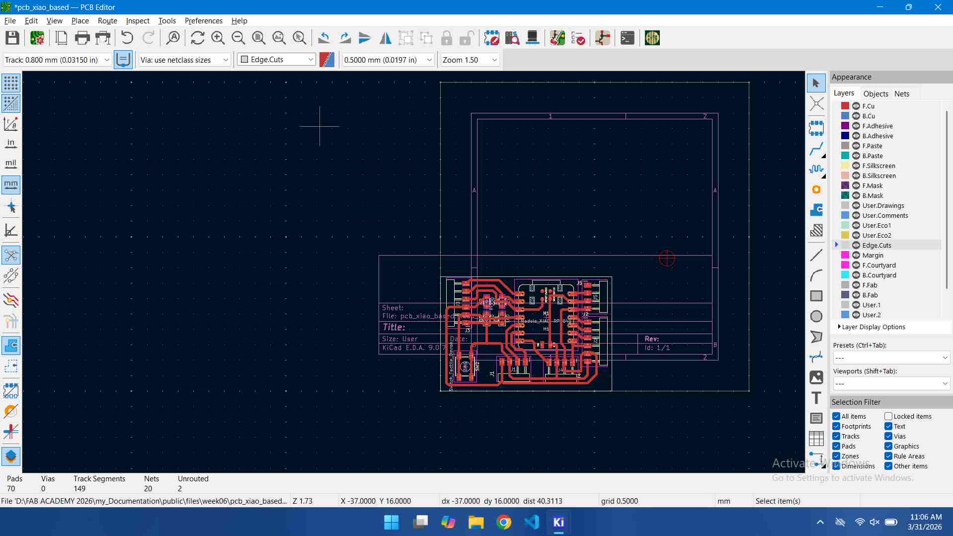
I finalized my PCB routing in KiCad, setting track widths to 0.6mm to survive high-speed isolation milling cleanly.
Preparing the Stock Board for Milling
Aligning the finalized layout design for export:
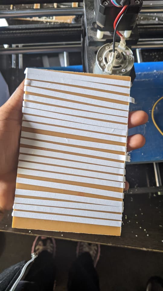
Applying heavy-duty double-sided tape onto the bottom of the FR-1 copper sheet to secure it tightly to the spoilboard, preventing bed vibration during spindle passes:
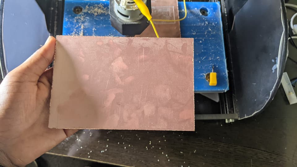
Positioning the prepared single-sided copper sheet firmly onto the CNC machine platform:
Generating Toolpaths Using Mods
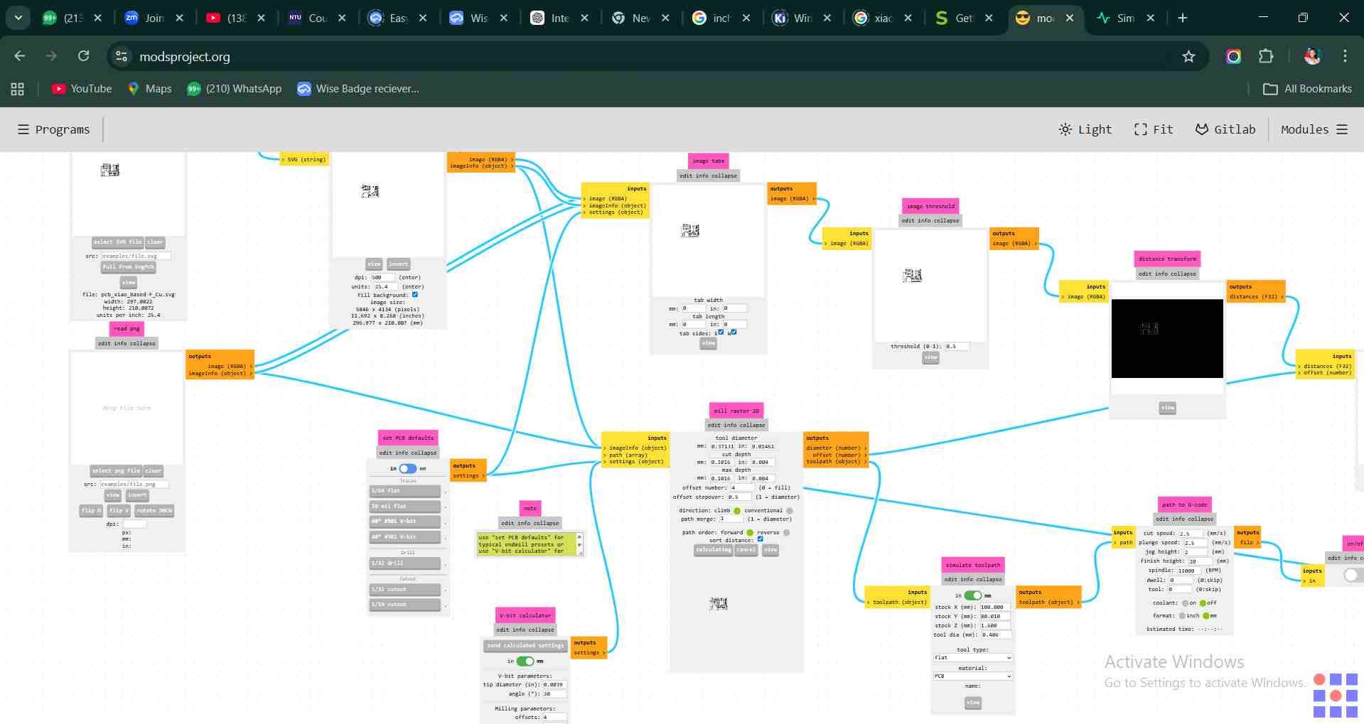
I imported the PCB SVG/PNG graphics into Fab Mods to generate toolpaths for isolation milling and contour cutting.
- Imported PCB design graphic into Mods.
- Set tool diameter (0.1mm V-bit angle) and cut depth parameters.
- Generated toolpath using
mill raster 2D. - Exported toolpath file as
trace.nc.
Setting up OpenBuildS CONTROL Software
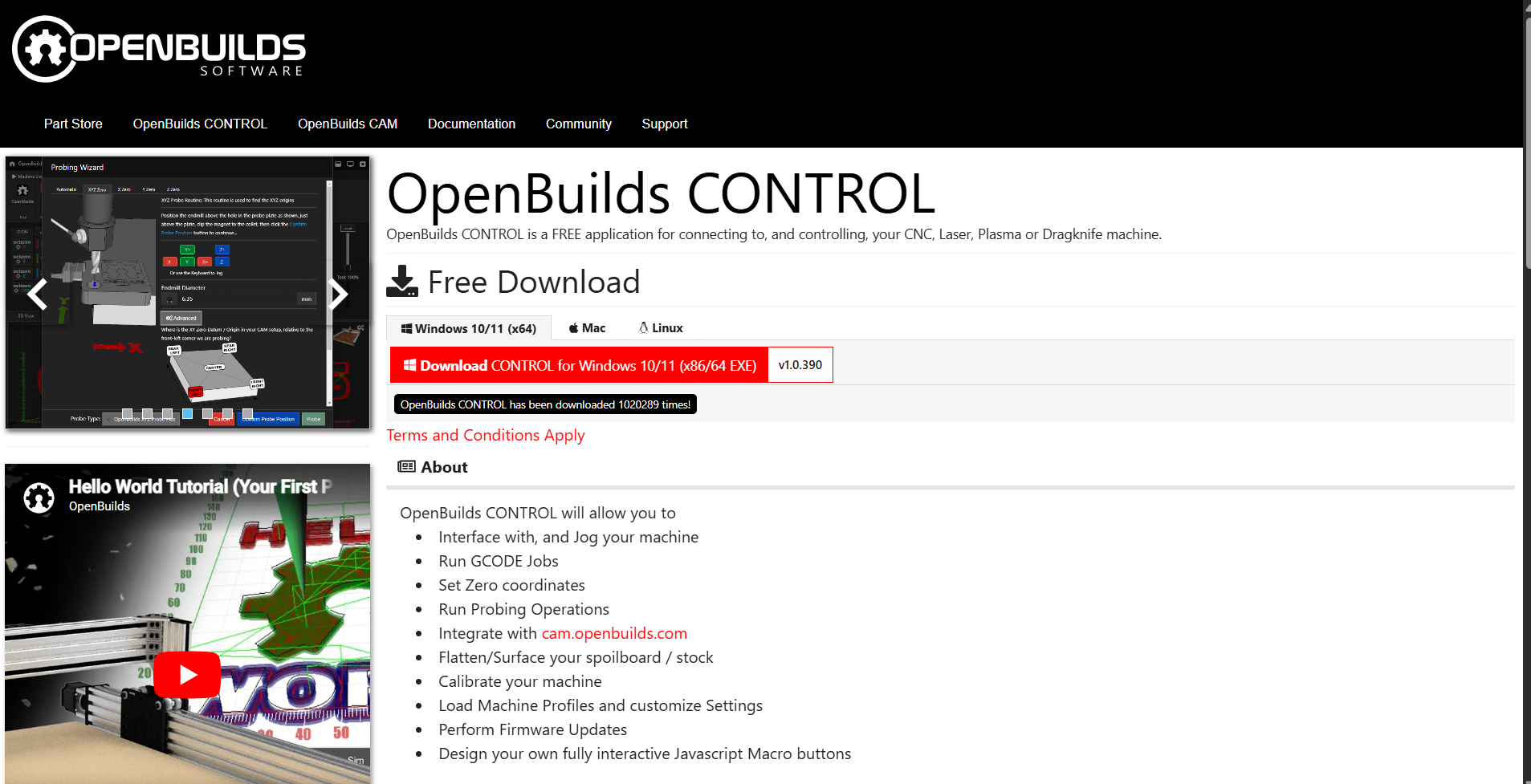
To control the desktop milling machine and execute the G-code, I installed the OpenBuildS CONTROL application.
Download OpenBuildS Software →
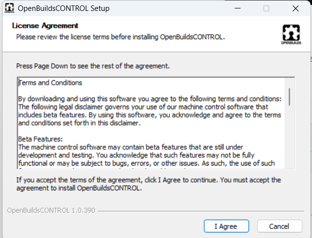
Accepted license agreements to proceed with installation setup:
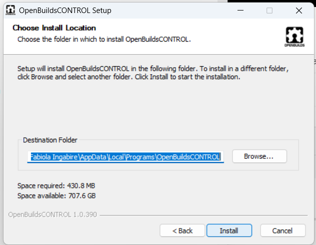
Selected the installation destination path on local disk storage:
Monitored installation completion progress:
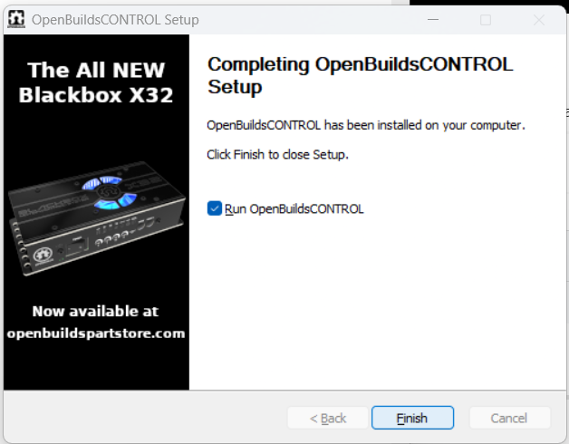
Completed application installation and launched OpenBuildS CONTROL:
Loading and Simulating G-code
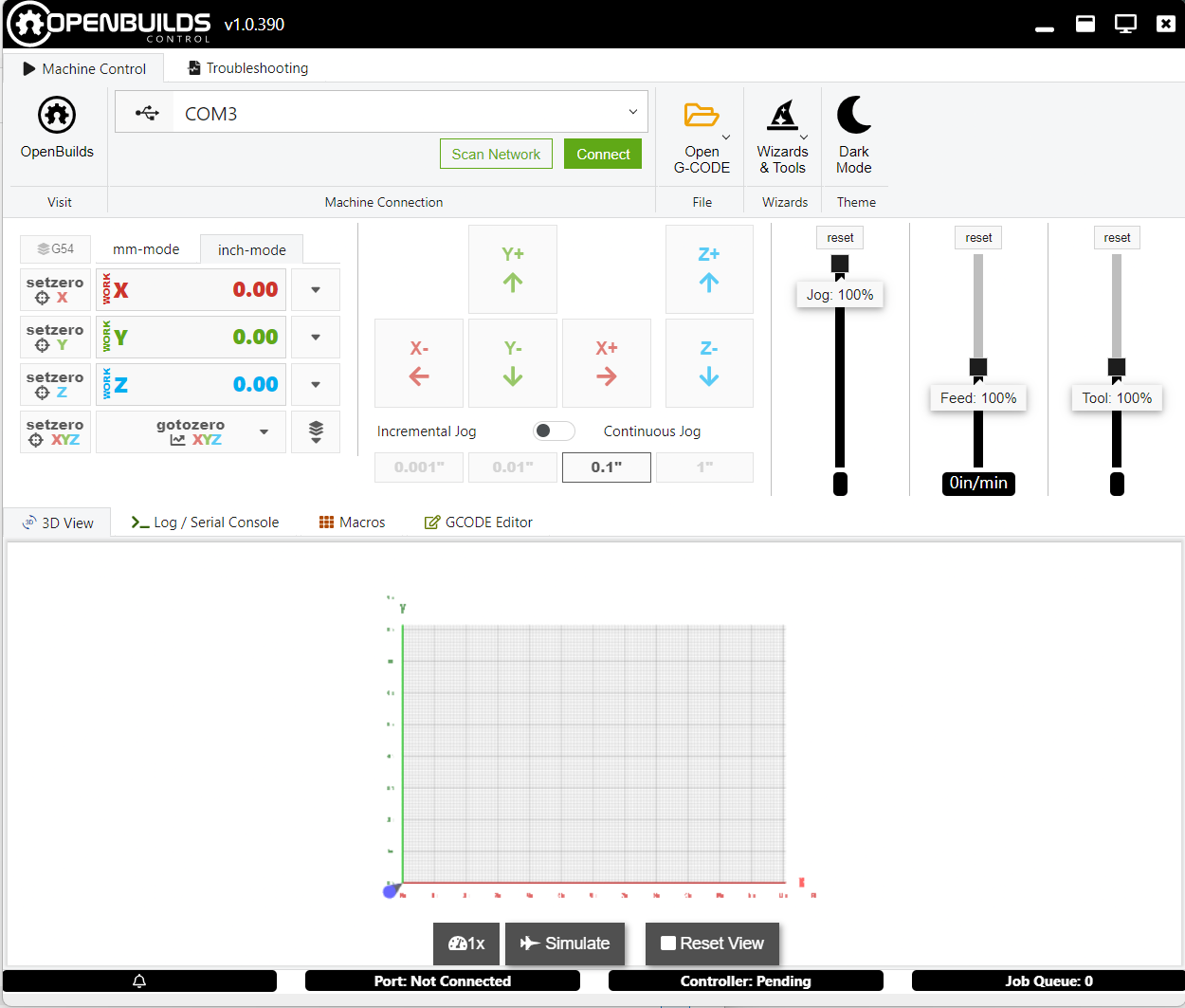
Opened the main CONTROL interface dashboard to initialize machine communication and toolpath previews:
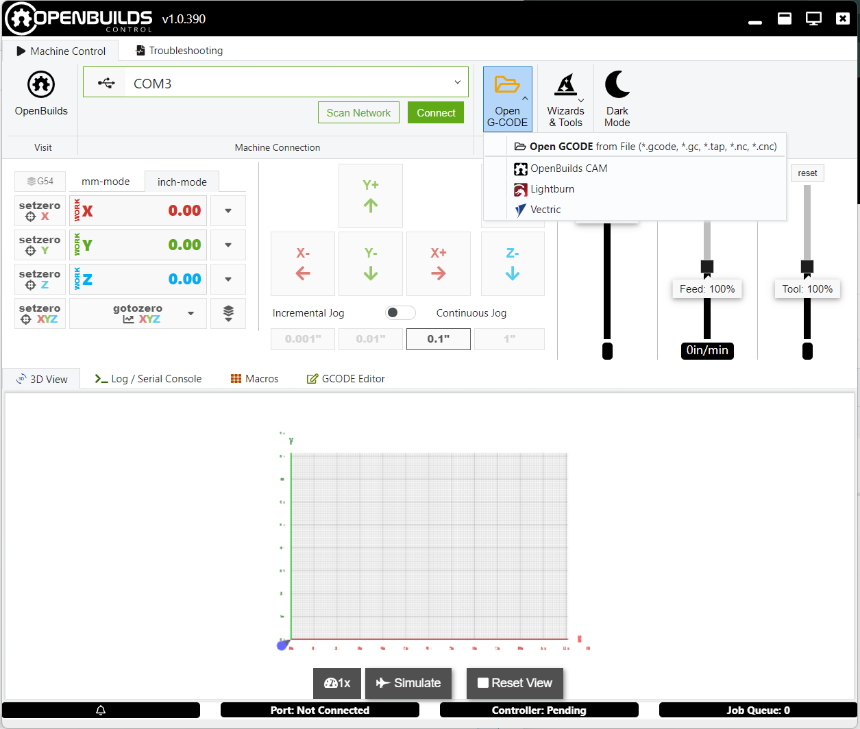
Clicked Open G-CODE in the main toolbar menu:
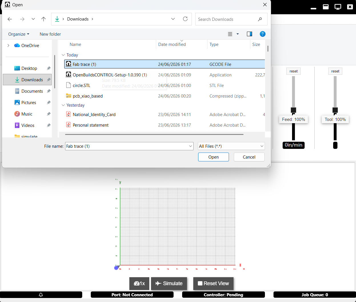
Selected the exported G-code toolpath file Fab trace (1).nc:
Verified the generated 3D visualizer toolpath layout overlaying the workpiece origin:
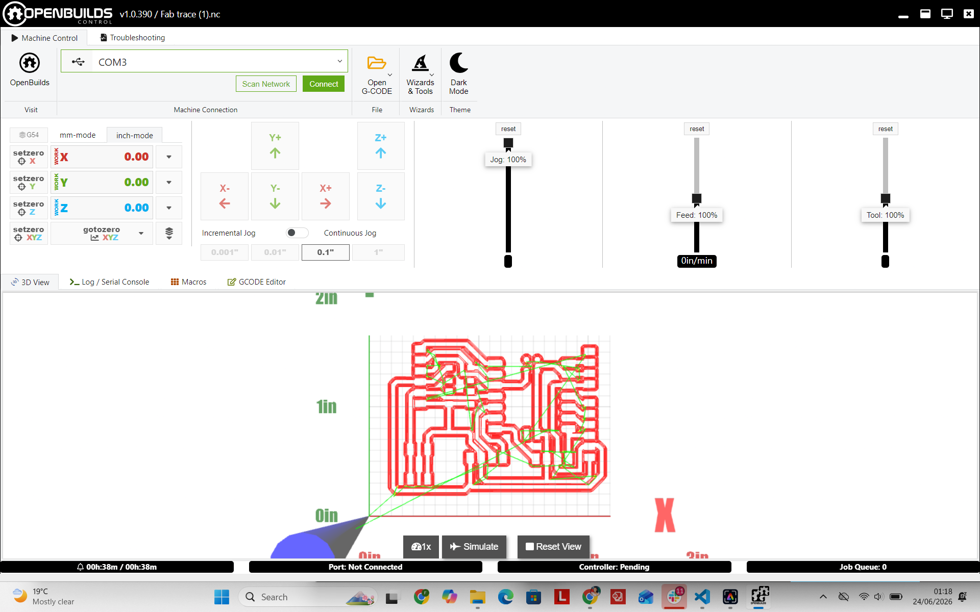
PCB Milling Simulation Video
Ran a dry simulation path to confirm toolhead clearance bounds prior to cutting copper:
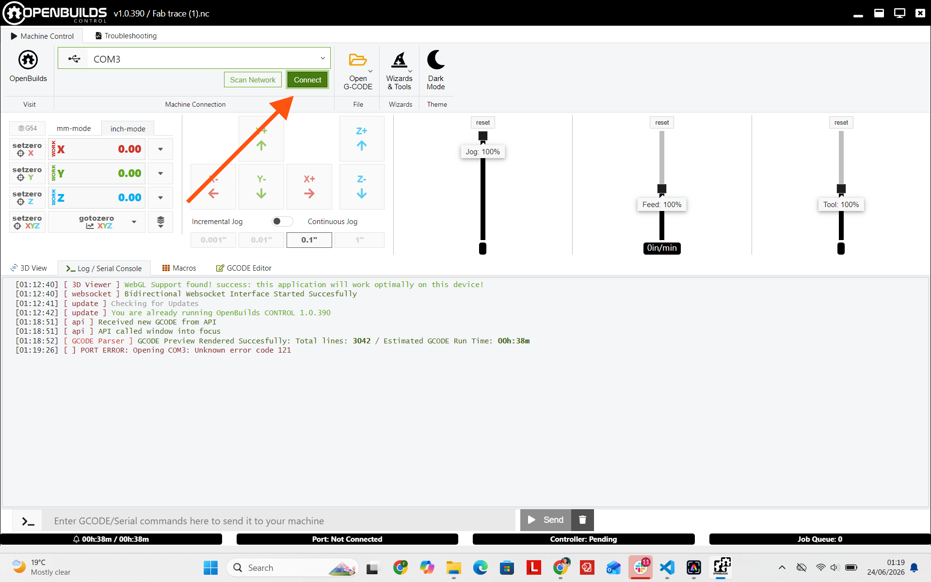
Connected the computer to COM3 port. Resolved an initial "Unknown error code 121" port error by re-seating USB controller cables:
Machine Setup & Z-Zeroing
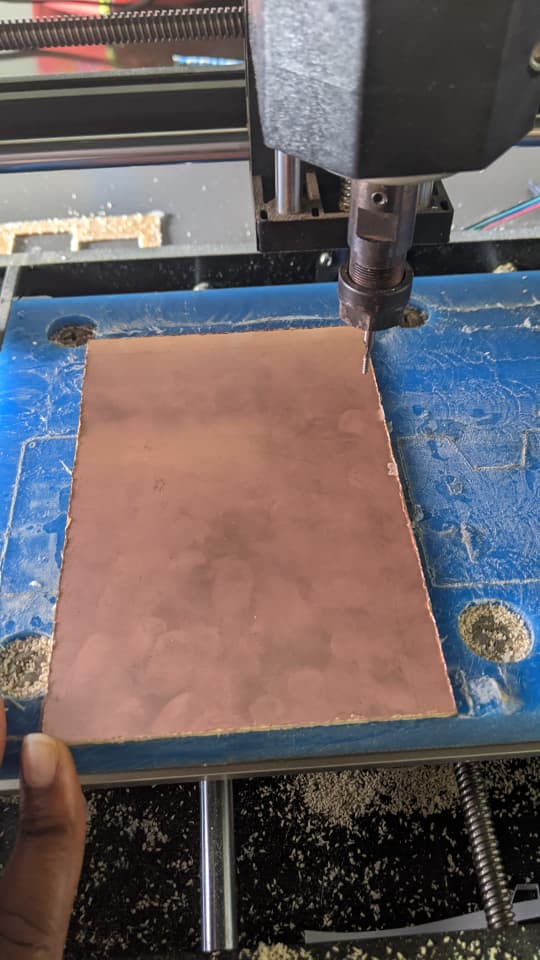
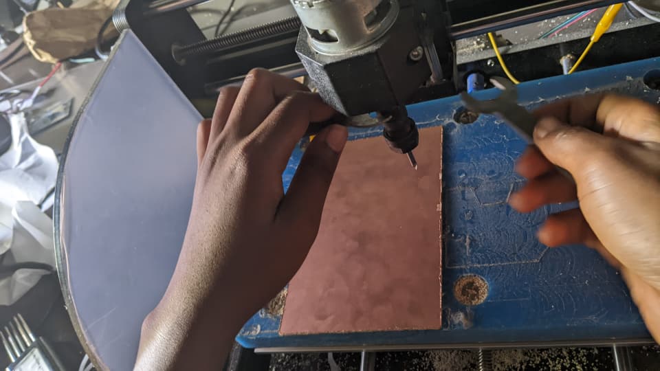
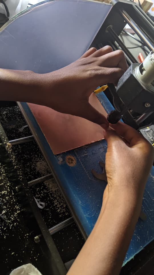
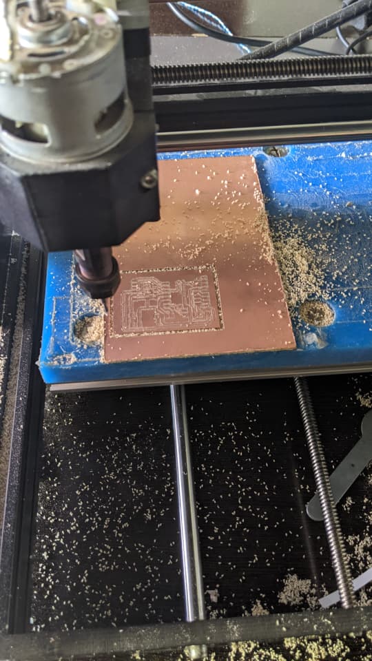
Secured stock board onto the sacrificial bed layer and installed the 0.1mm V-bit into the collet using dual wrenches. Set Z-zero precisely so the bit tip makes physical contact with the copper plane surface without gouging.
Milling the Isolation Traces
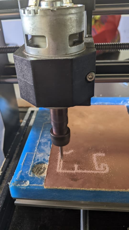
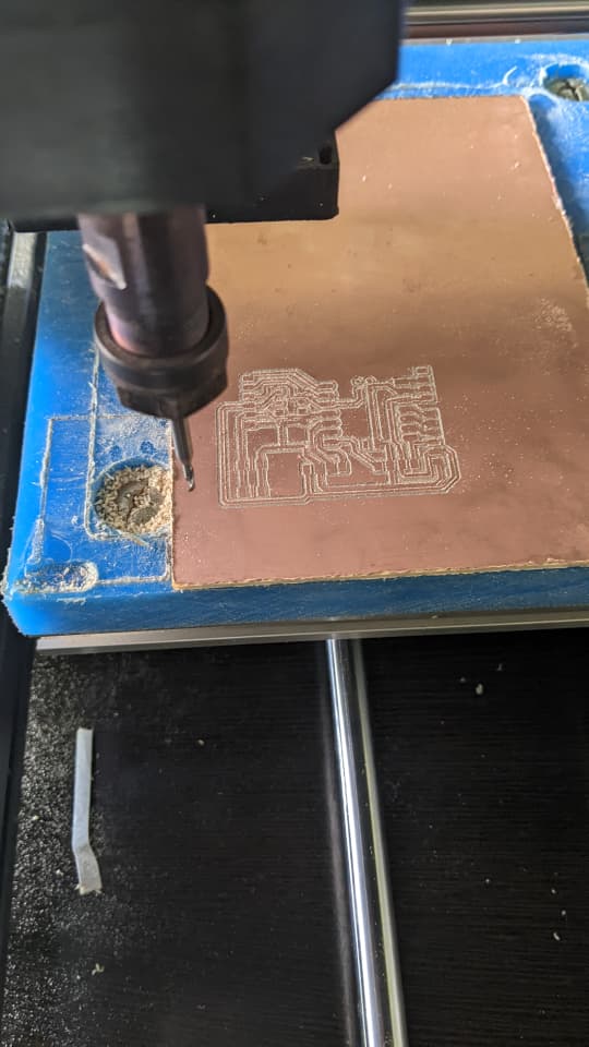
Executed G-code toolpaths to engrave isolation paths and separate traces on the board surface:
Cutting Board Outline
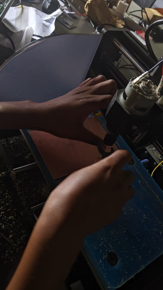
Replaced the V-bit engraver with a 1.0mm flat end mill to execute the profile cutout file, freeing the milled board from raw FR-1 stock.
Soldering & Assembly (Stuffing)
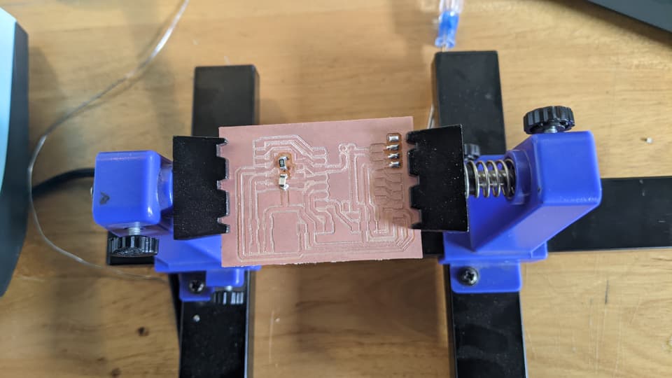
Soldered surface-mount passive components first, installing SMD LEDs and current-limiting resistors:
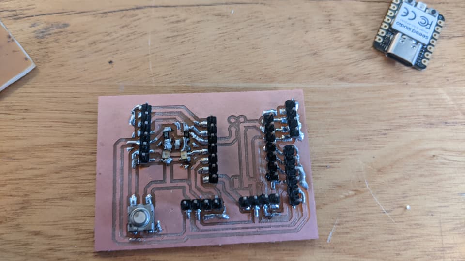
Soldered pin headers and mechanical pushbuttons:
Final Assembly
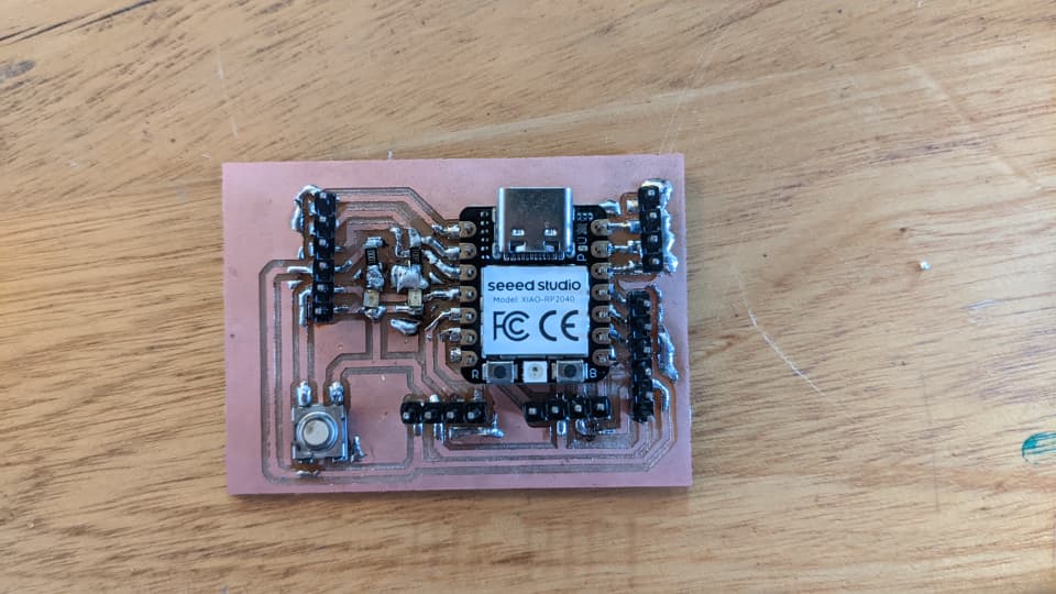
Mounted the XIAO RP2040 core module onto the breakout header sockets:
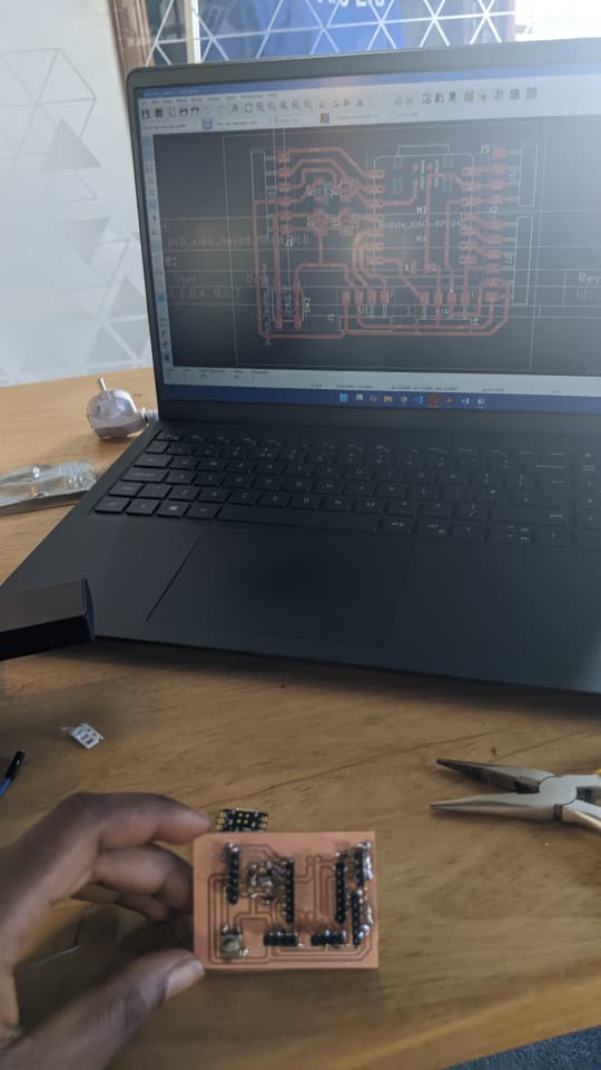
Programming & Hardware Testing
Uploaded an Arduino C++ blinking test program to verify GPIO output routing. The LED toggled correctly, confirming power delivery, clean solder joints, and working microcontroller pin continuity.
PCB Operational Testing Video
Acknowledgment
Special thanks to our local facilitator for explaining PCB milling operation principles, optimal feed rates, and guiding trace width scaling. Thanks also to my lab peers for sharing troubleshooting insights during machine setup.
Challenges & Problem Solving
Problem: Initial KiCad layout used a 0.4mm trace width. Facilitator feedback advised increasing trace widths to minimize tear-outs during isolation milling.
Solution: Increased trace width by 0.2mm (scaling from 0.4mm up to 0.6mm), yielding robust copper tracks.
What I Learned
- The critical importance of spoilboard leveling and Z-zeroing for consistent trace depth.
- Managing iron heat during soldering to prevent lifting delicate milled copper pads.
- Generating isolation toolpaths while accounting for bit tip geometry to avoid short circuits.