// Week 04
Embedded Programming
Assignment Objectives
- Link and integrate individual work with the group assignment page.
- Explore and document key technical information from a microcontroller datasheet.
- Develop and program a board to interact using local inputs/outputs and UART communication protocol.
- Describe and document the complete programming workflow in a structured step-by-step format.
- Include and present well-structured source code in a clean and readable format.
- Capture and present final hero shots demonstrating the working system and achieved outcomes.
Tools & Technologies
Microcontroller Unit (MCU):
ESP32 Dev Module (32-bit Xtensa Dual-Core LX6 Processor)
Local Input/Output Interface Devices:
2x Tactile Push Buttons (Inputs), 1x Red LED (Output), 1x Green LED (Output), 2x 220Ω Current-Limiting Resistors
Software, Pipelines & Communication Protocols:
Wokwi Web Emulation Toolchain, Arduino IDE compiler core, GPIO register manipulation, UART serial communication protocol
Individual Assignment Documentation
1. Group Work Reference & Core Learning
As part of this week's exploration, I collaborated with my peers to compare embedded toolchains across different chip architectures—specifically an 8-bit AVR (ATmega328P) and a 32-bit Xtensa dual-core ESP32 platform.
You can review the full testing workflow and comparative analysis on our Group Assignment documentation.
2. Microcontroller Datasheet Summary (ESP32)
Key technical specifications extracted from the ESP32 datasheet are summarized below:
| Parameter | Value | Notes |
|---|---|---|
| Operating Voltage | 2.2V – 3.6V (3.3V Typical) | Standard internal operating range |
| CPU / Core | Xtensa® Dual-Core 32-bit LX6 | Clock speed up to 240 MHz (600 DMIPS) |
| Memory | 520 KB SRAM / 4 MB Flash | Internal SRAM and external SPI Flash storage |
| Wireless Connectivity | Wi-Fi 802.11 b/g/n & Bluetooth 4.2 BLE | Integrated 2.4 GHz RF transceiver subsystem |
| Peripheral Interfaces | GPIO, ADC, DAC, UART, SPI, I2C, PWM | Multiplexed software-configurable pin matrix |
Selected Pin Mapping: GPIO 2 (Red LED), GPIO 4 (Green LED), GPIO 15 (Button 1), GPIO 18 (Button 2).
3. Programming Workflow
- Architecture Analysis: Identified safe GPIO pins from the ESP32 datasheet.
- Circuit Design: Built and tested input/output wiring inside the Wokwi simulator.
- Firmware Development: Wrote Arduino-based control logic targeting pin registers.
- Compilation & Upload: Converted C++ code into binary binaries and deployed to MCU.
- Testing & Debugging: Verified logic states and data telemetry using serial monitor log output.
4. Emulated Prototyping & Circuit Design
The system was first planned and implemented within a web-based simulation environment to eliminate hardware risks during early prototyping. The development process began by adding core interface peripherals to the canvas.
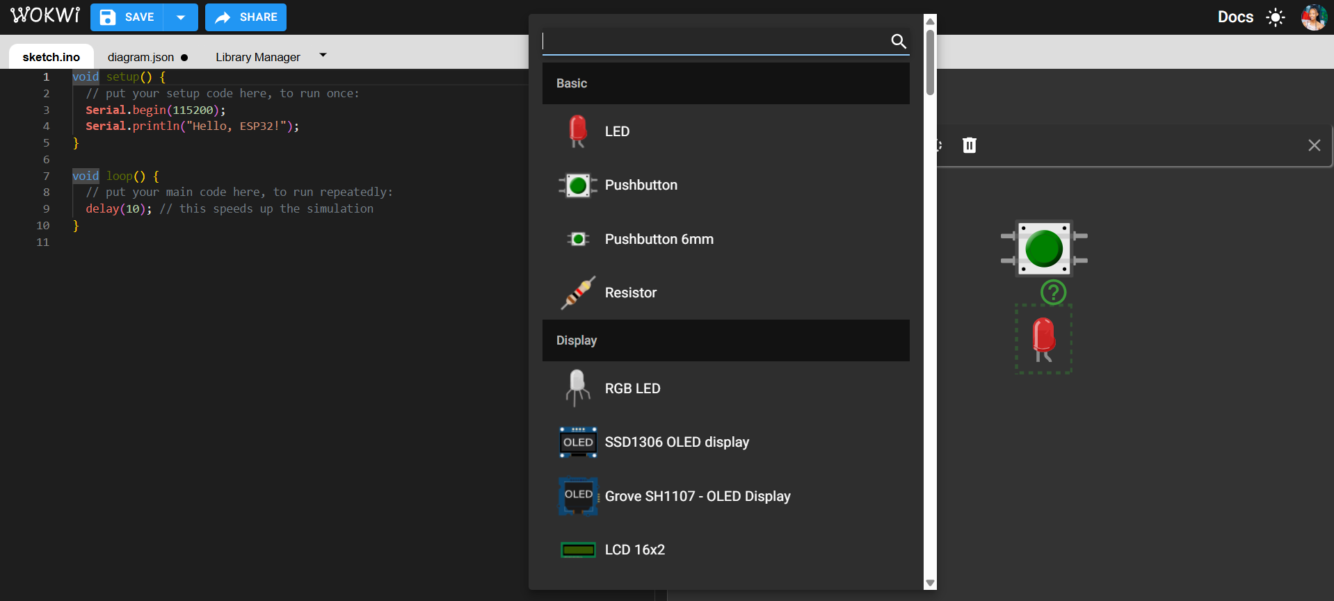
Figure 1: Sourcing fundamental I/O assets including tactile pushbuttons, current-limiting resistors, and light-emitting diodes from the emulation tray.
Before wiring the electrical nodes, I thoroughly analyzed the manufacturer's pinout diagram to confirm functional channel limitations. To prevent dynamic boot loop issues, I carefully cross-referenced strapping pins and avoided sharing logic lines with standard hardware configuration lines.
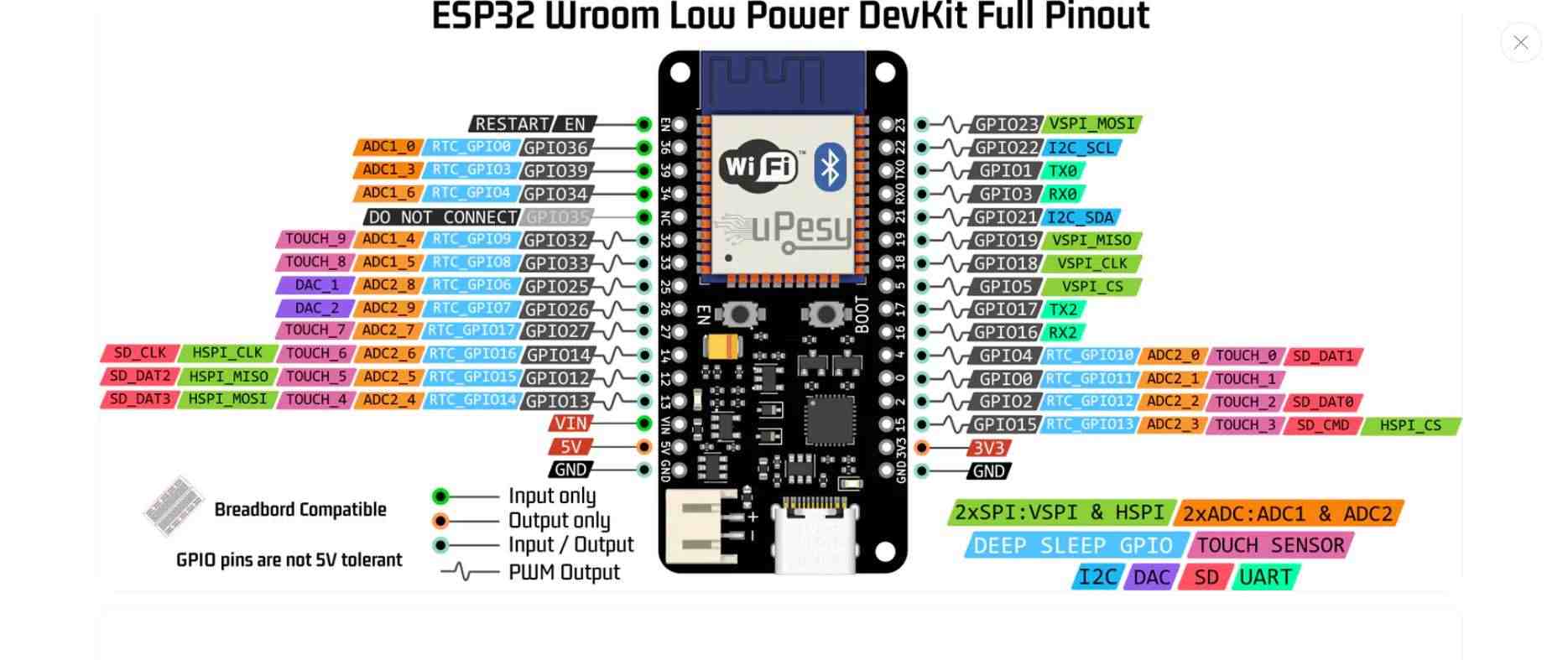
Figure 2: Manufacturer reference pin map highlighting peripheral matrices and identifying standard 3.3V power rails.
Using the reference mapping data, push buttons were tied directly between their respective GPIO pins and common Ground lines. By enabling internal pull-up structures (INPUT_PULLUP) within the chip's firmware, input signals are securely anchored High when floating, and transition cleanly to a low logical state when depressed.
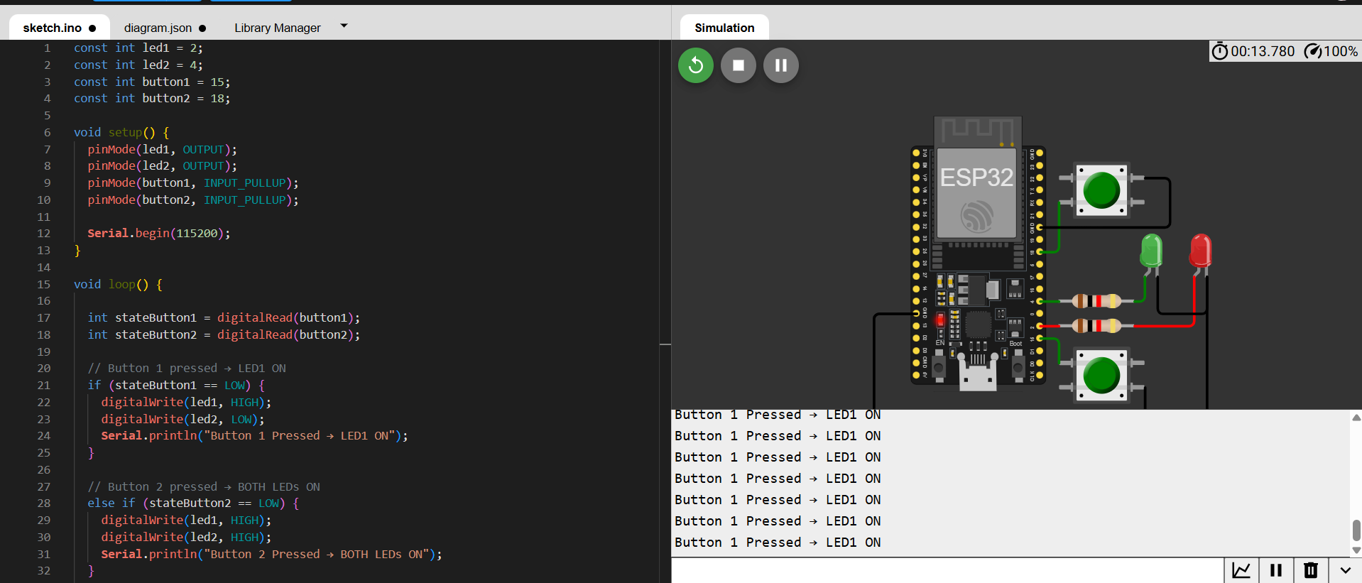
Figure 3: Completed schematic matrix layout illustrating explicit pin connections and inline current-limiting buffers.
5. Embedded Application Source Code
The firmware below implements local I/O interaction loops alongside active wired data communication protocol streaming over UART at a 115200 baud rate:
const int redLed = 2;     // Digital Output mapped to Red LED
const int greenLed = 4;   // Digital Output mapped to Green LED
const int button1 = 15;   // Digital Input for Switch 1
const int button2 = 18;   // Digital Input for Switch 2

void setup() {
  pinMode(redLed, OUTPUT);
  pinMode(greenLed, OUTPUT);

  pinMode(button1, INPUT_PULLUP);
  pinMode(button2, INPUT_PULLUP);

  Serial.begin(115200);
  Serial.println("--- System Initialized. Awaiting Input Operations ---");
}

void loop() {
  int state1 = digitalRead(button1);
  int state2 = digitalRead(button2);

  if (state1 == LOW) {
    digitalWrite(redLed, HIGH);
    digitalWrite(greenLed, LOW);
    Serial.println("[PROTOCOL DATA] Button 1 Triggered -> Local State: RED LED ACTIVE");
  }
  else if (state2 == LOW) {
    digitalWrite(redLed, HIGH);
    digitalWrite(greenLed, HIGH);
    Serial.println("[PROTOCOL DATA] Button 2 Triggered -> Local State: DUAL LED ENERGIZED");
  }
  else {
    digitalWrite(redLed, LOW);
    digitalWrite(greenLed, LOW);
  }

  delay(100);
}
6. Wired Communication Testing & Verification
By initializing the serial transport terminal layout at 115200 baud, I validated successful asynchronous data transfer logs. Pressing individual simulation elements instantly pushes targeted state packets over the serial transport pipeline, allowing me to isolate and verify each distinct interactive loop behavior step-by-step.
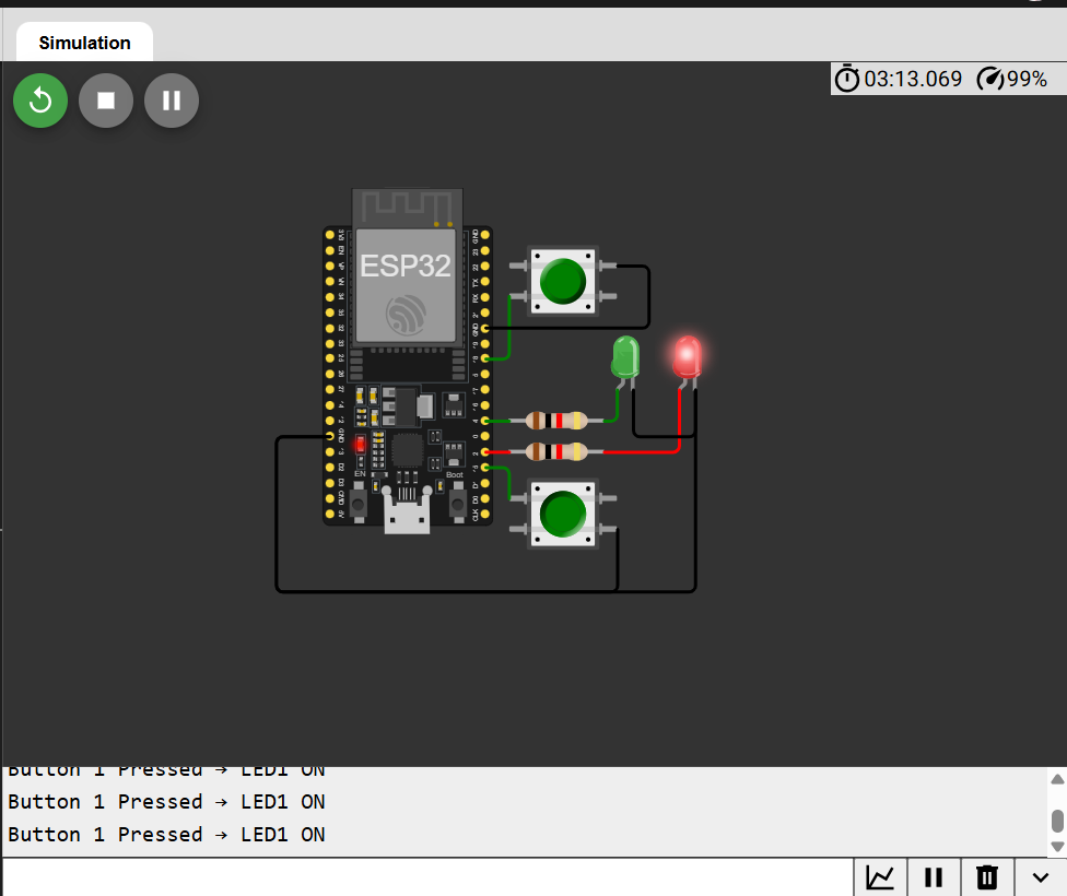
Figure 4: Testing Interaction Loop 1. Engaging Button 1 cleanly drives the Red LED line high and broadcasts corresponding telemetry data.
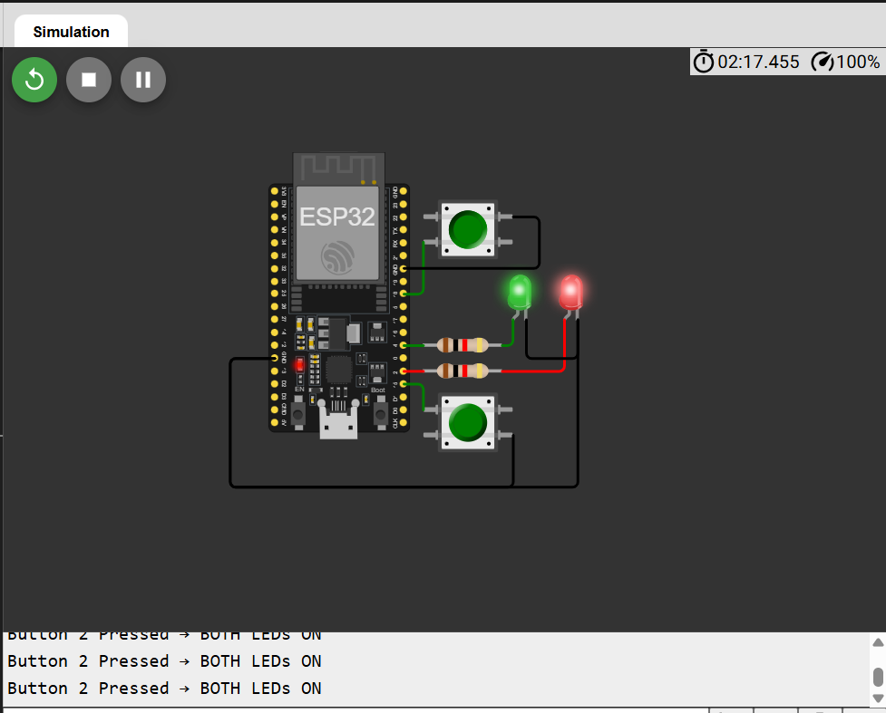
Figure 5: Testing Interaction Loop 2. Engaging Button 2 successfully energizes both output channels concurrently while streaming diagnostic packets.
7. Production System Hero Shots
Below is the completed functional setup. It captures responsive output adjustments based on active input interactions, along with corresponding monitoring streams tracking operational routines.
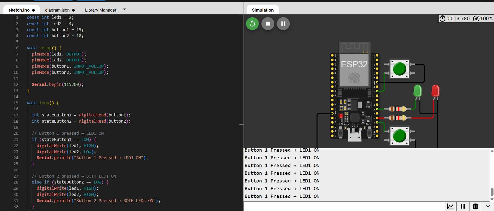
Figure 6: Final operational system Hero Shot displaying responsive LED arrays executing concurrently with UART diagnostic data streams.
Challenges & Problem Solving
No fatal hardware compilation errors arose during the development layout passes. During early pin-muxing stages, special attention was required to isolate traditional strapping pins (like GPIO 12 or GPIO 0) to keep them clear of external pull-up components. This ensured the microcontroller wouldn't get stuck in flash or alternate boot loops when cycling power.
Reflection
This assignment enhanced my understanding of building interactive firmware environments around real physical microchip topologies. Exploring manufacturing datasheets transformed from a simple reading task into a vital engineering step for pin layout discovery. Mastering GPIO register states and tracking telemetry parameters via serial monitoring tools forms a reliable baseline for debugging more complex embedded projects.
What I Learned
- Interpreting electrical configurations and peripheral matrices directly from microchip datasheets.
- Implementing internal software
INPUT_PULLUPlines to cleanly anchor logic states. - Developing responsive code structures to process data across concurrent hardware devices.
- Deploying wired UART communication protocol frameworks at high transmission speeds (115200 baud).