
Input Devices: Group Assignment
Characterizing Analog Levels and Digital Signals using Laboratory Test Equipment
1. Objectives & Setup
The group objective for this week is to observe, test, and characterize the real-world electrical behavior of an input device's analog levels and digital signals. For our group benchmark testing, we selected the MQ135 Gas Sensor module interfaced with our custom microcontroller development board running a Seeed XIAO RP2040.
Test Bench Instrumentation:
- Oscilloscope: RS Pro IDS-2202E Digital Storage Oscilloscope (200 MHz, 1 GS/s)
- Digital Multimeter: UNI-T UT139C True RMS Digital Multimeter
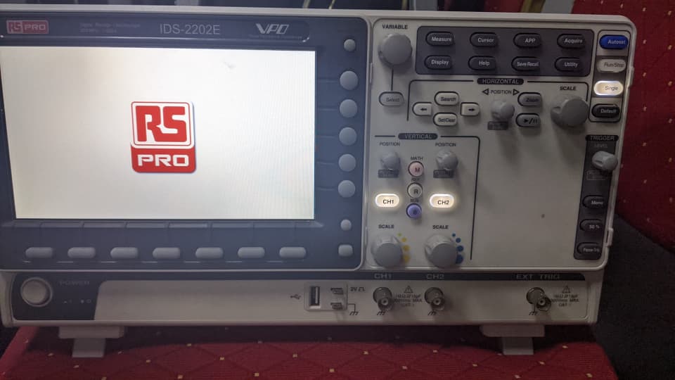 Figure 1: Initializing the RS Pro IDS-2202E Digital Storage Oscilloscope at the test bench.
2. Probing with the Oscilloscope (RS Pro IDS-2202E)
We began our evaluation by booting up the RS Pro oscilloscope and establishing a clean measurement baseline to inspect our signals.
Step 1: Signal Setup & Channel Configuration
We utilized Channel 2 (CH2) on the oscilloscope for our sensor tests. The ground alligator clip of the probe was attached directly to our board's central GND plane, and the hook tip was initially applied to the Analog Output (AO) line of the MQ135 module.
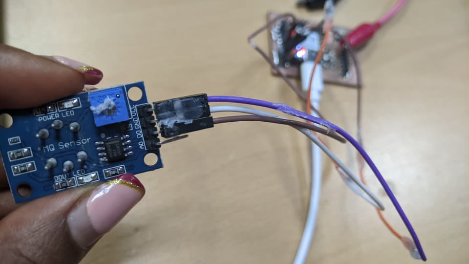 Figure 2: Pin interface configuration on the MQ135 sensor module showing VCC, GND, DO, and AO pins.
Step 2: Signal Scaling Optimization
When first probing the line, the waveform output was compressed and jumping outside of our default grid limits, making it impossible to perform precise data analysis.
To fix this, we modified our scaling settings. We turned the CH2 Volts/Div knob to cleanly center the $3.3\text{V}$ maximum peak to fit neatly inside the screen grid squares and modified the Time/Div knob to perfectly track live changes without signal clipping.
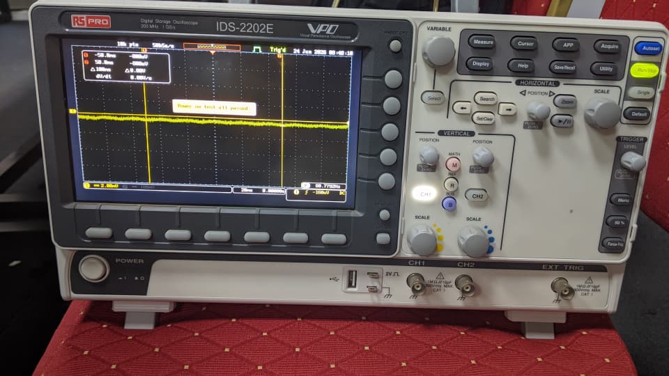 Figure 3: Main dashboard of the oscilloscope adjusted with optimized vertical and horizontal grid parameters.
Step 3: Analyzing Analog vs. Digital Signals
A. Analog Output (AO) Characterization
Probing the AO pin showed a continuous, responsive wave voltage. When environmental gas concentrations shifted, the signal moved across a continuous smooth curve, illustrating a true analog behavior perfectly captured across our scaled horizontal timeline.
B. Digital Output (DO) Characterization
Next, we moved the probe tip to the Digital Output (DO) pin. Unlike the smooth adjustments observed on the analog pin, the digital signal behaved like a clear step function—instantly transitioning between absolute Low ($0\text{V}$) and absolute High ($3.3\text{V}$) states once the onboard comparative threshold dial was crossed.
3. Measuring Steady-State Signals with the Multimeter
To verify the true DC steady-state values calculated by our MCU and displayed on the oscilloscope, we deployed our UNI-T Digital Multimeter set to DC Voltage mode ($V\overline{\dots}$).
We placed the black common probe on our board's GND pin and touched the red probe directly to the sensor interface lines to observe real-time variations:
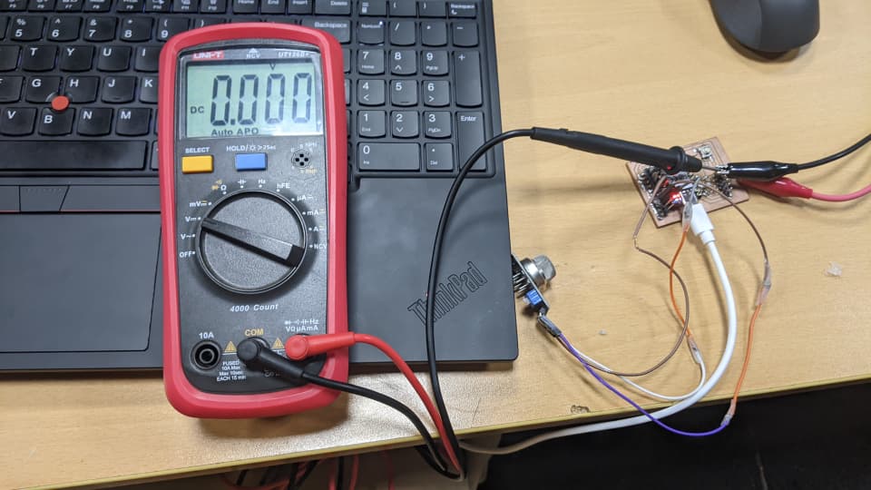 Figure 4: Direct probing of steady-state voltage values using the UNI-T UT139C Multimeter.
- Baseline Testing: In standard baseline conditions, the multimeter reported a steady reading hovering around $0.004\text{V}$ to $0.005\text{V}$ on the digital output lines.
- Dynamic Response Tracking: When changes were introduced, we monitored the digital voltage jump cleanly up to our target system reference level ($3.3\text{V}$ range), validating the structural accuracy of our input hardware interfaces.