Week 15: System Integration
Introduction
This week, I will focus on building the main board for my final project as well as designing and manufacturing the enclosures for all the electronic components. An important part of the process will also be creating a sketch of the final product so I can better imagine how the complete system will look and function once assembled.
In general, my project consists of a boxing training device equipped with three step-response sensors designed to measure both reaction time and striking speed. The idea is for the system to detect the user’s response after receiving a visual signal and then record the corresponding timing data for analysis.
To improve the interaction and visual feedback of the device, I will also incorporate NeoPixel LED strips, which will provide lighting cues and make the training experience more dynamic and engaging. The entire system will be controlled using an ESP32-WROOM-32, which will handle sensor readings, timing calculations, and wireless communication within the project.
The Neopixels strips and ESP32 will need enclosures to keep them in place and safe, I the sketch I will also include the paths for the wires to pass and keep order.
Electronic Design & Production
Design
Schematic
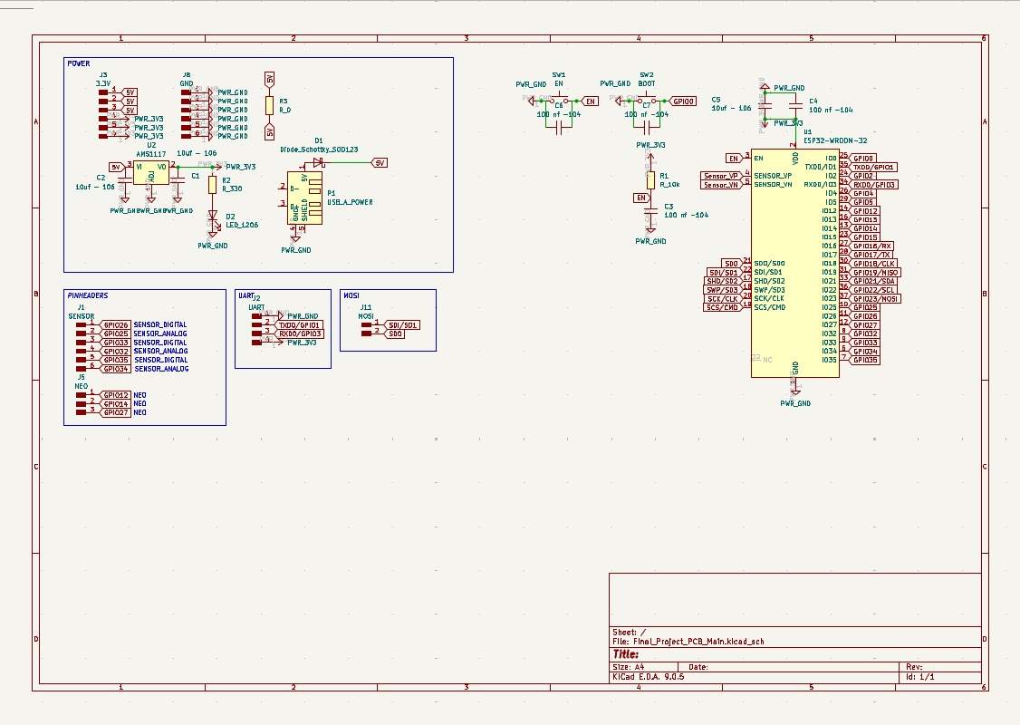
Power
Power
• To power my circuit, I’ll use a 5V, 3A wall charger, so I connected it to my board via a USB Type-A cable, using only the VCC and GND pins. I intended to use a Schottky diode to protect my circuit; however, my professor Oliver told me that it would significantly reduce my voltage and that the regulator would be sufficient, so I won’t use it when soldering and will instead place a 0-ohm resistor.
Next, I installed an AMS1117 regulator from 5V to 3.3V, placing two 10uF capacitors on the input and output. Then, on the 3.3V output, I placed an LED connected to a 2000Ω resistor to provide a visual indication that it is powering correctly. Finally, I added 3 5V pins and 3 3.3V pins to power my NEOPIXELS and sensors, respectively, and I also added 6 ground pins for the same purpose. The 0-ohm resistor is there to facilitate the connection in the design.
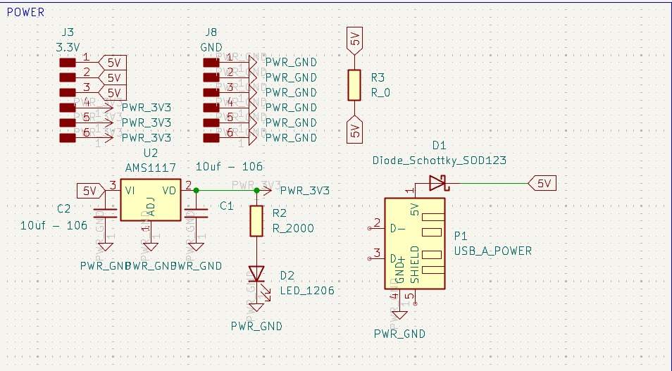
ESP32 WROOM 32
ESP32 WROOM 32
• The ESP32 WROOM 32 is connected to 3.3V via two capacitors in parallel—one 10uF and the other 100nF—to prevent voltage spikes that could impair the chip's functionality. I installed two buttons, Boot and Enable; both are connected to the ESP32 and to GND via a 100nF capacitors. The capacitor has this value to ensure precise signal transmission. The Enable pin is also connected to a 10k resistor and a 100nF capacitor to GND.
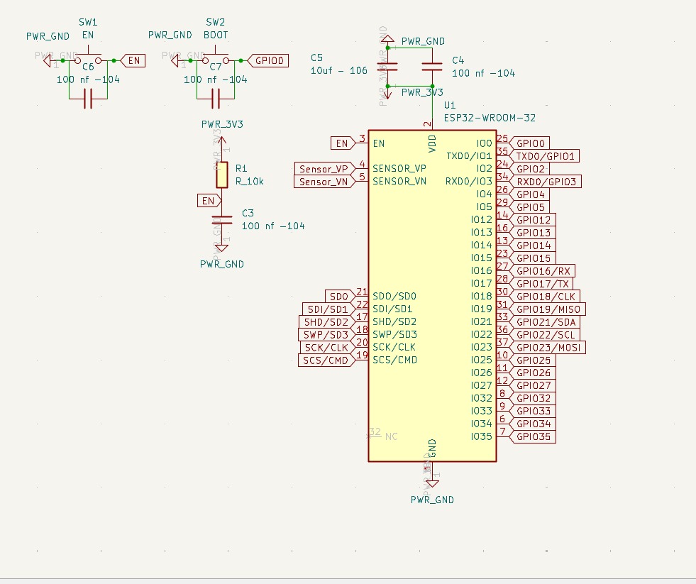
PINS
PINS
• The pins are for the three analog sensors, which require four connections (VCC, GND, Input, and Output). Then there are three for the Neopixels (VCC, GND, VIN, VOUT). I also included pins for UART communication so I can program my board, and I left pins for MOSI.
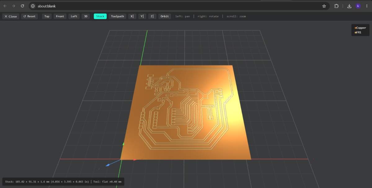
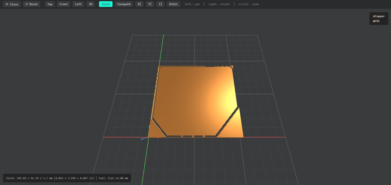
PCB Design
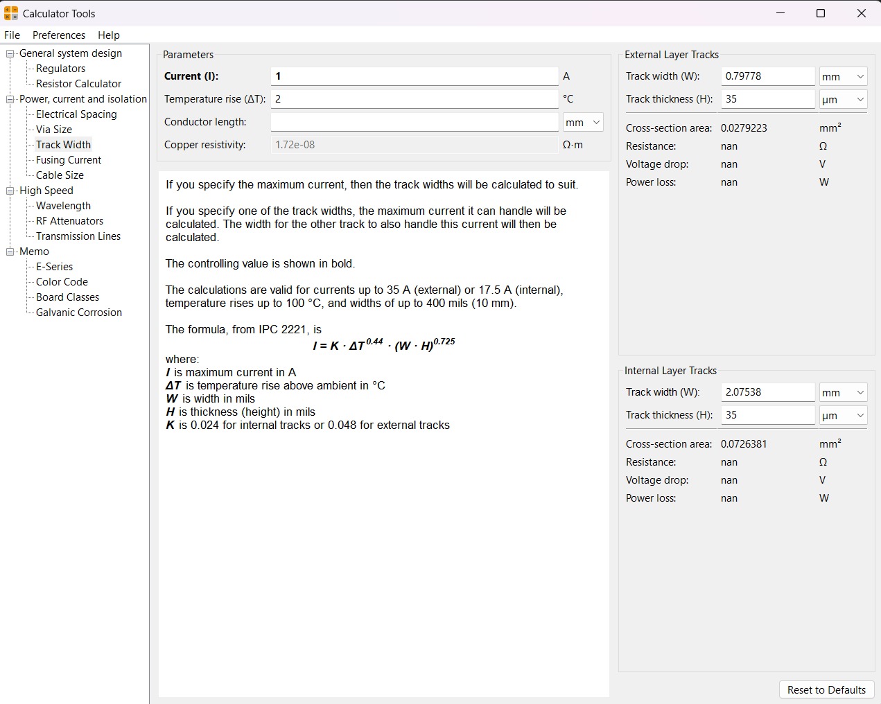
Calculator tool. Before defining the size, it is important to calculate it using the calculator tool given by KiCad. To do that we first have to go to the start menu and open the Calculator tool.Then add the Current (I) and the Temperature rise we are expecting our PCB to have and look fo the result the calculator will give back to us in the right top side. The calculator works by using a formula explained at the bottom.
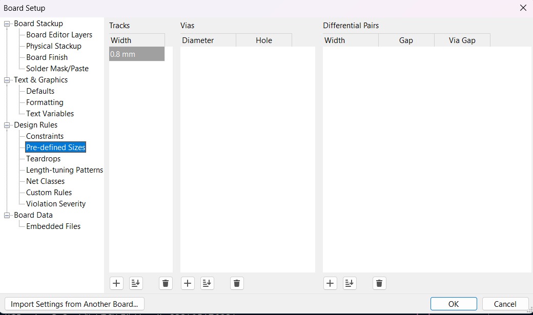
Track thickness. To change the track thickness we must go to the top tool section and click on Track use netclass width. Subsequently, select Edit Pre-defined Sizes.
Inside that section we can add tracks sizes by clicking the + symbol located at the bottom of the window, and in the width section we can change the width of the new track we added. Then we'll just have to click Ok.
Design
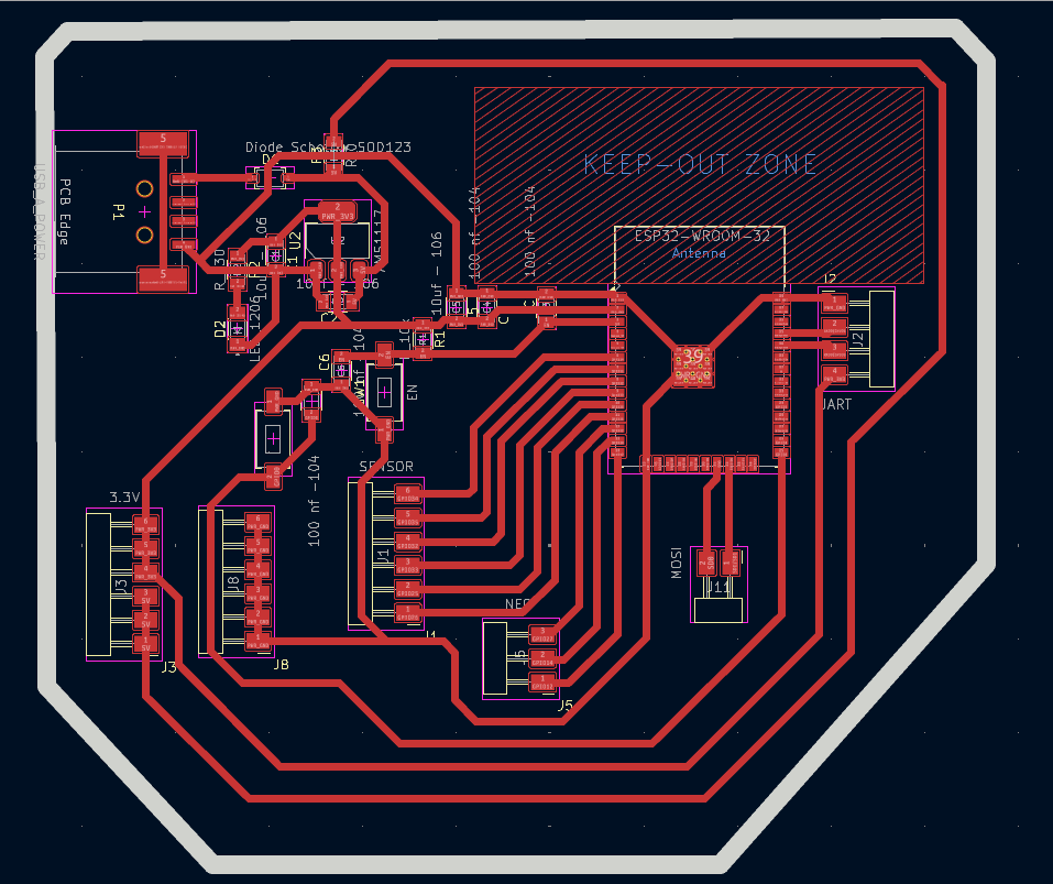
After using KiCad’s width calculation tool, 0.8 mm trace width was selected. I placed the USB at the edge of the board so it would be easier to connect it, then I tried to place all the pins that will be connected to external components as close as posible so I can have more order and I also left the signal space free so it won't be interrfered. The enable and boot buttons are close so I can program it easier.
Parameters. • The outline width is 2 mm and its layer is Edge.Cuts. • The track’s width is 0.8 mm and its layer is F.Cu.Results
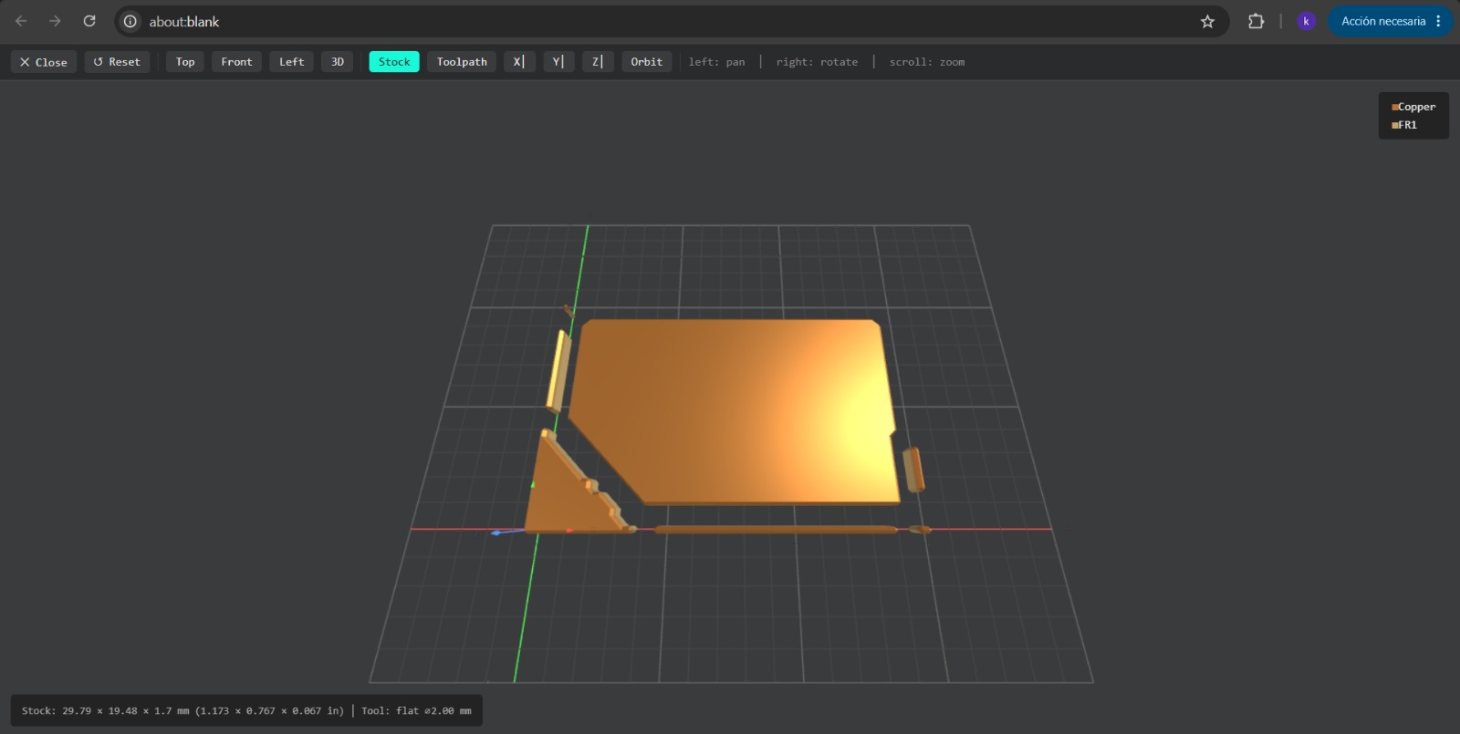
Export as SVG
1. First, I changed the border line width to 2 mm because of the tool that will be used later.
2. Then I went to the top left corner and pressed file, after that I selected Fabrication Outputs.
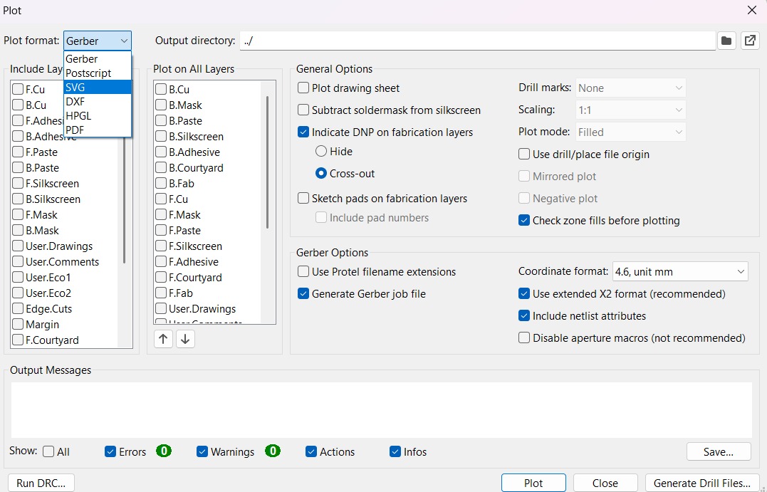
3.In the fabrication outputs we have to select Gerbers. In Gerbers we have to change the plot format to SVG.
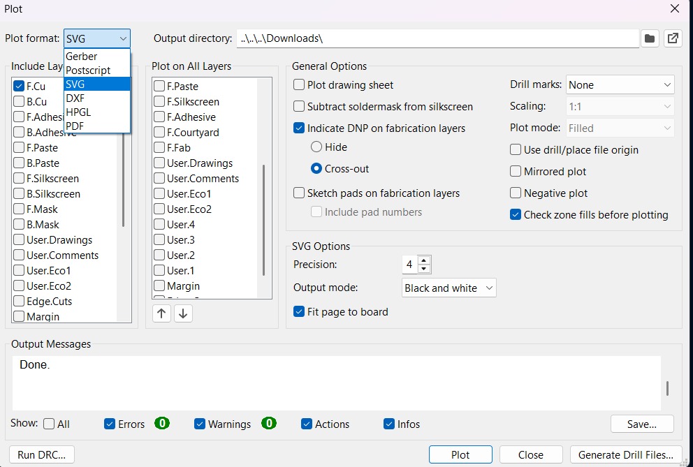
4.Having changed the format to SVG, we have to click on Fit page to board to keep the meassures the way they are in the dessign and select the Output Directory.
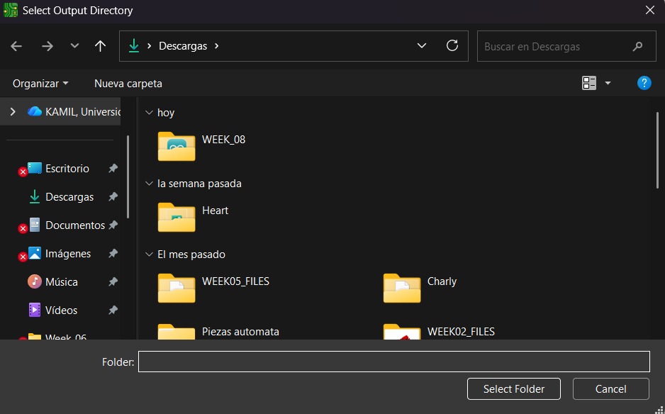
Output Directory To change the Output Directory we have to click on the folder symbol located at the top and select the place in our computer where we want to save our document.
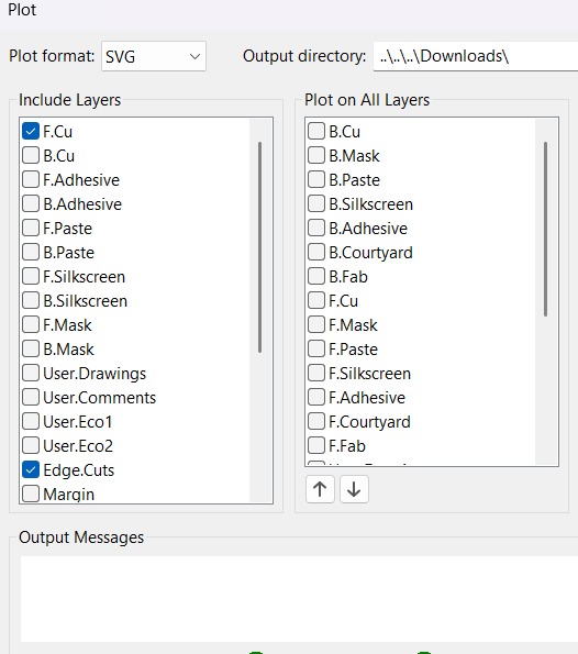
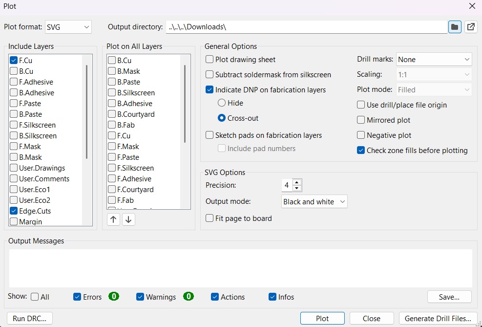
5. Then, we have to select the layers we want to plot.
6. Finally, we have to click on plot and go to the folder where our files are located.
Before Cutting
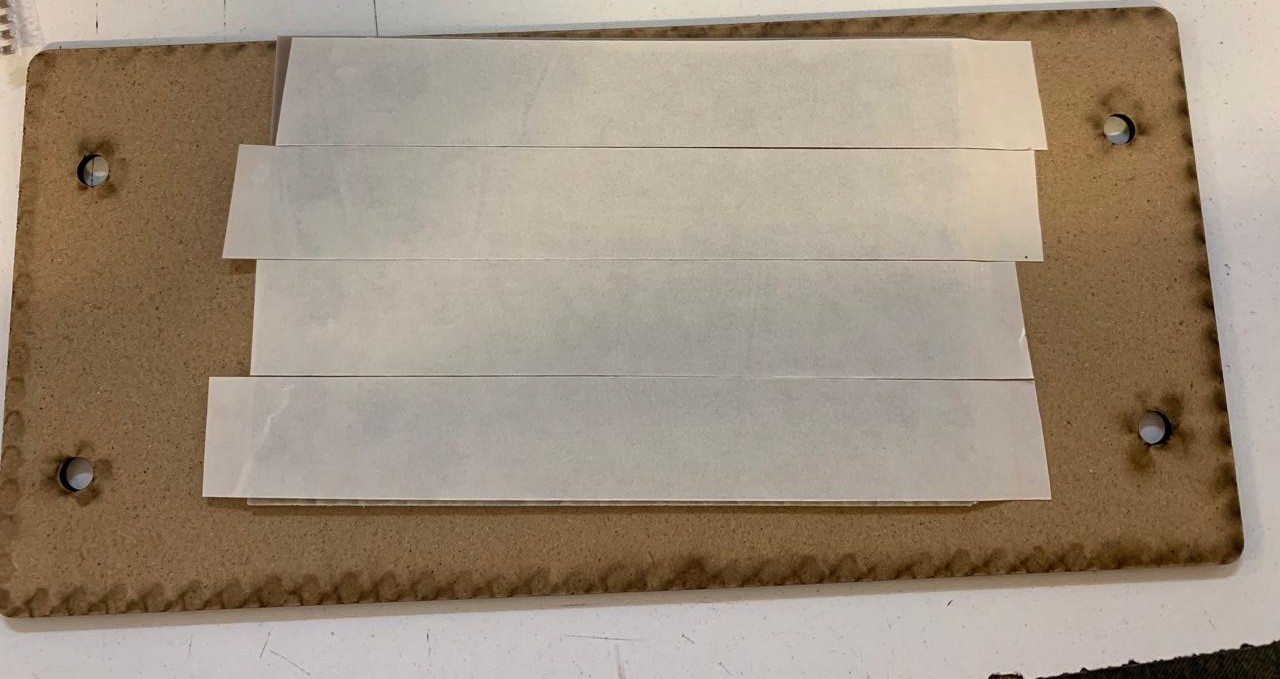
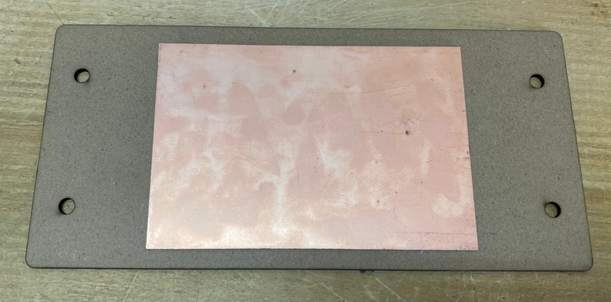
1. First, we have to paste the tape in the back of the copper board.
2. Then, we have to paste the copper board to the Sacrifice Bed.
Materials:
Copper Board.
double-sided tape.
Sacrifice Bed. Is an MDF board designed to prevent the SMR-20 from being damaged in the event that the tool drills too deep.
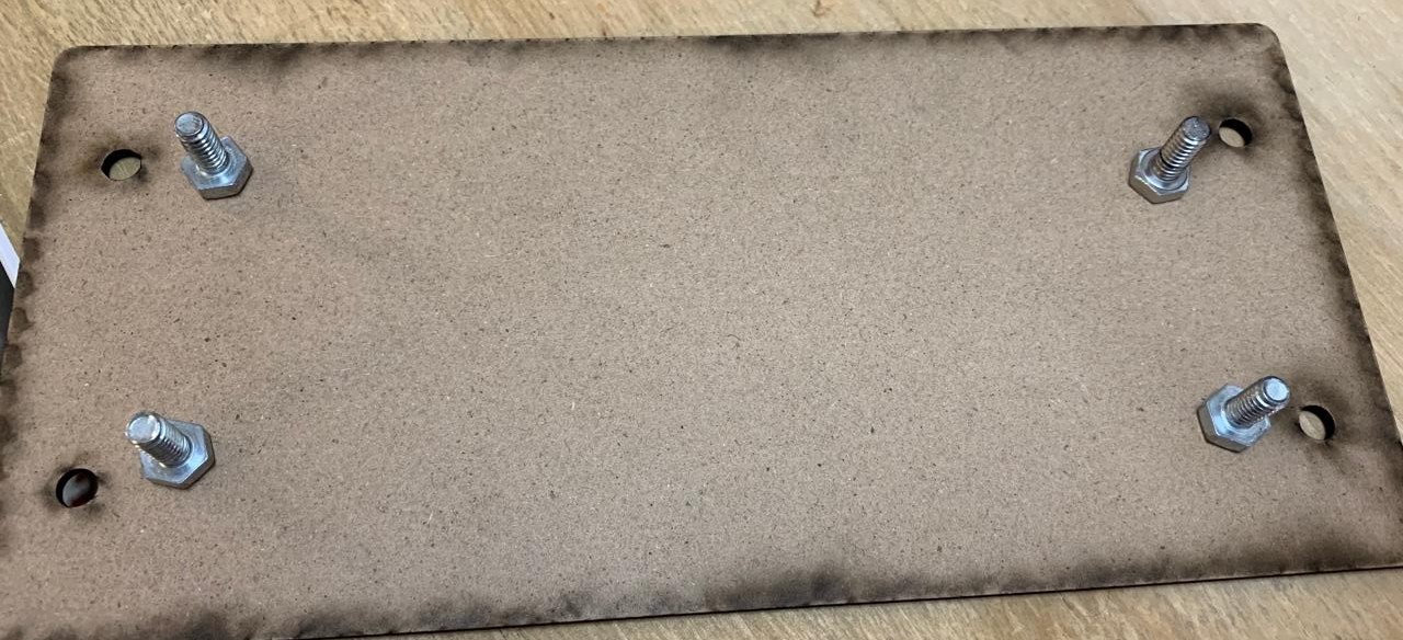
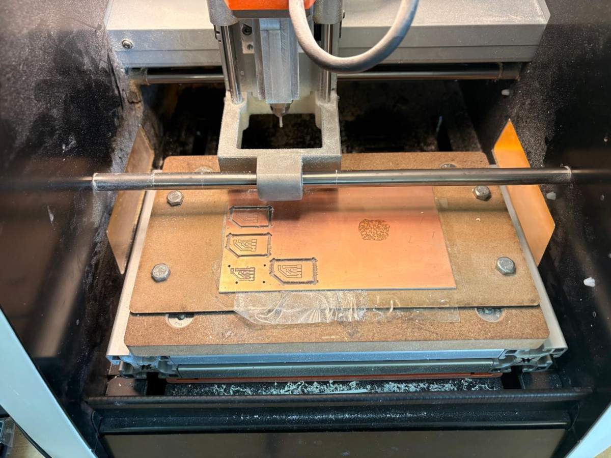
3. Subsequently, we have to place the bed inside the SMR-20. In my case, in my lab, our SMR-20 has a fitting to secure the sacrifice table with screws.
Before Cutting
4. Having secured the bed inside the SMR-20, we have to select the tool for each milling process (Tracks and Borders).
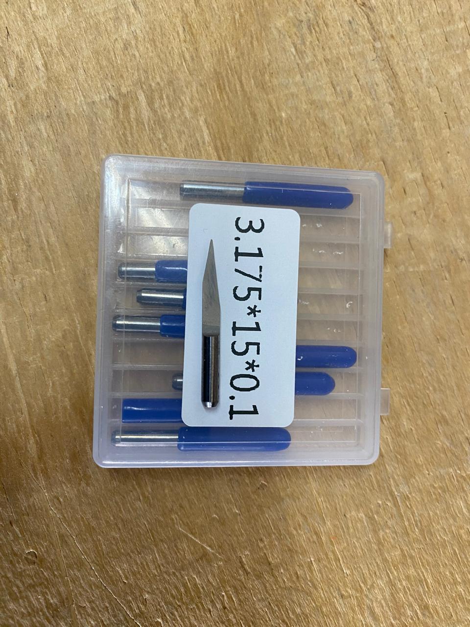
Cutting tool. This tool is specifically designed for traces, as its point is sharp and very thin. The Speed of use can be higher but we must be careful about its deep.
Cutting - MODS.
Tool width. 0.39 mm
Speed. 4 mm/s
Origin (x,y,z). (0,0,0)
Offset number. 3
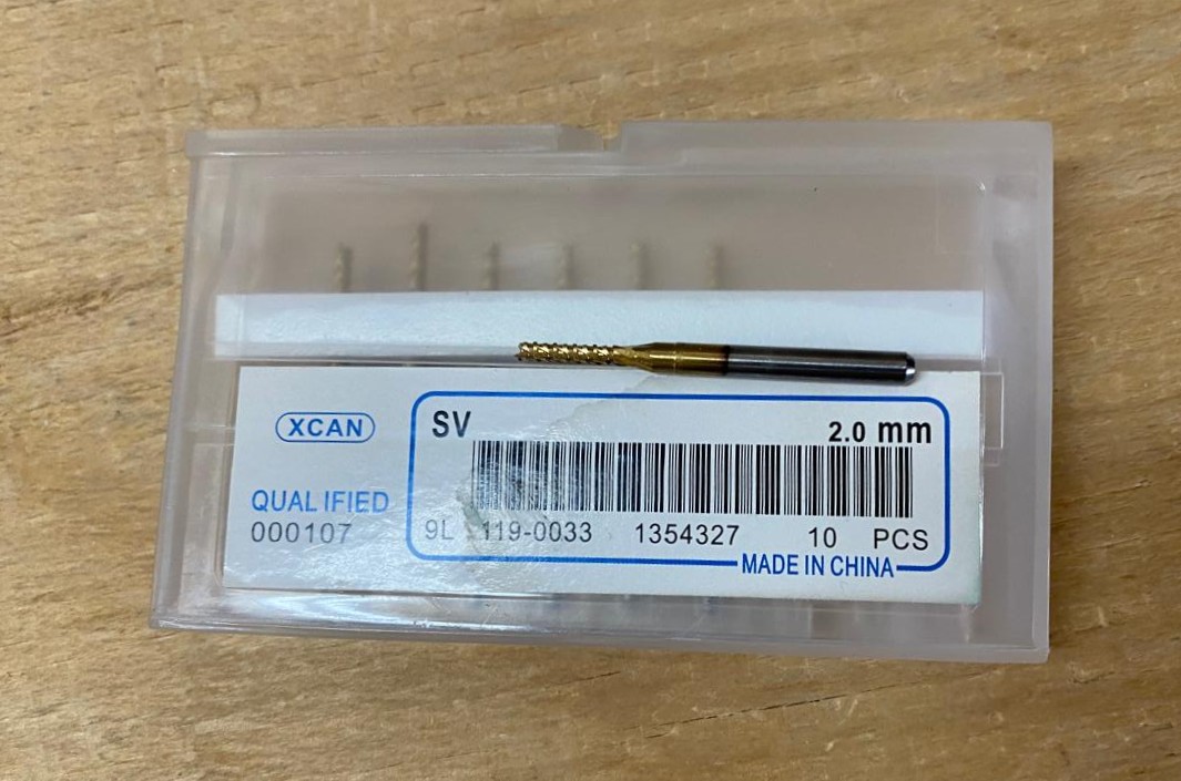
Outline tool. This tool is can be used for the border cutting because of its width, it can also be used for perforation, but the diameter of them will be bigger.
Outline - MODS.
Tool width. 2 mm
Speed. 4 mm/s
Origin (x,y,z). (0,0,0)
Offset number. 1
Cutting
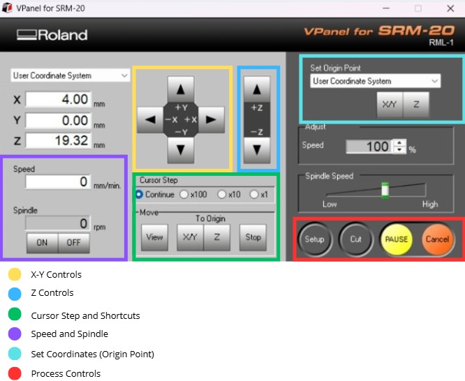
1. We have to connect our computer to the SMR-20 and open VPANEL.
VPANEL.
X-Y Controls. Move the tool in the X-Y axis.
Z Controls.Move the tool in the Z axis.
Cursor Step and Shortcuts. The Step Cursor determines the speed at which the tool moves along all axes; Continue is the smoothest and x1 is the slowest setting, since each click corresponds to a single motor movement. The Shortcuts are to automatically move to an already saved point (Origin Point).
Speed and Spindle. Is to set the speed and to turn on or turn off the the spin of the tool.
Set Coordinates (Origin Point). By clicking the XY or the Z button we can set the Origin Point.
Process Controls. Cut is for adding our code and start the process. Pause, this allows you to pause the process and resume it from where it left off. Stop, stops the process.
Cutting
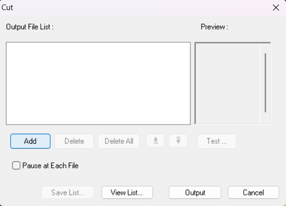
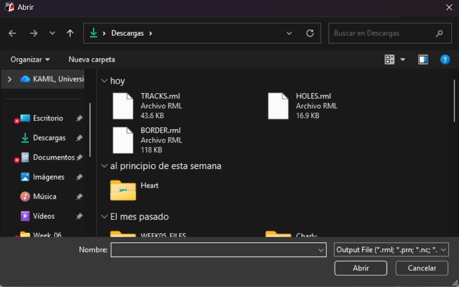
2. Then we have to click on Cut. A window will open, and we should click Add to add our milling code.
3. Finally we have to click Output and the machine will automatically start to cut.
After Cutting
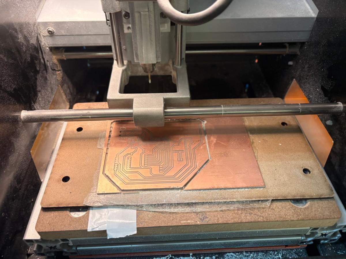
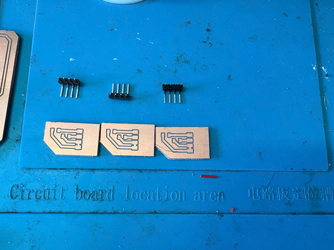
1. After finishing the cutting, very carefully, we must take out the copper board and remove our PCB.
Design
Schematic
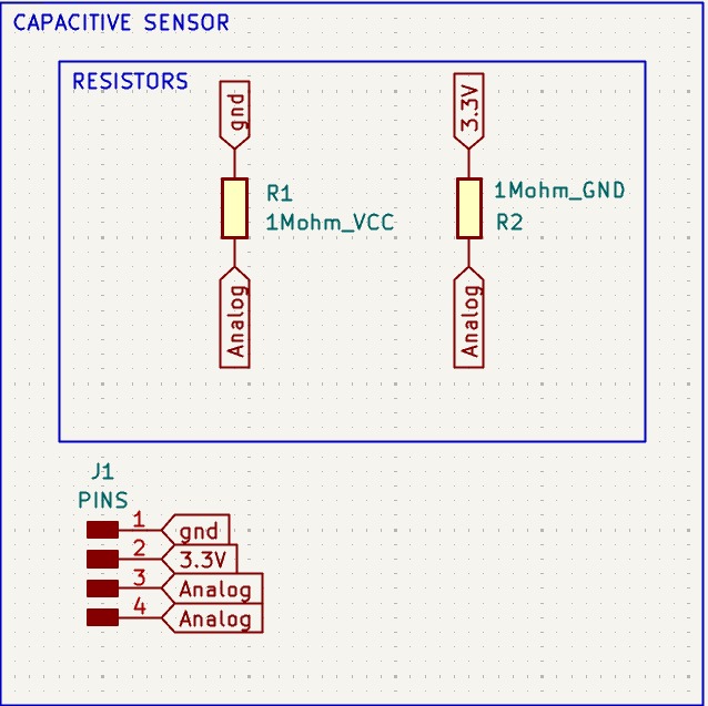
Capacitive Sensor
Capacitive Sensor
• I simply connected two 1M resistors, each connected to 3.3V and GND, respectively. Then I connected four pins for VCC, GND, the analog output, and the pin that connects to a step response sensor board.
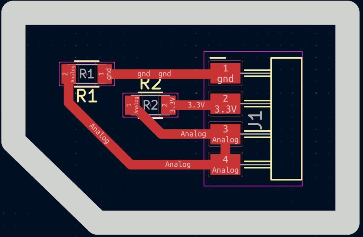
PCB Design
Calculator tool. Before defining the size, it is important to calculate it using the calculator tool given by KiCad. To do that we first have to go to the start menu and open the Calculator tool.Then add the Current (I) and the Temperature rise we are expecting our PCB to have and look fo the result the calculator will give back to us in the right top side. The calculator works by using a formula explained at the bottom.
Track thickness. To change the track thickness we must go to the top tool section and click on Track use netclass width. Subsequently, select Edit Pre-defined Sizes.
Inside that section we can add tracks sizes by clicking the + symbol located at the bottom of the window, and in the width section we can change the width of the new track we added. Then we'll just have to click Ok.
Design
After using KiCad’s width calculation tool, 0.8 mm trace width was selected. I placed the USB at the edge of the board so it would be easier to connect it, then I tried to place all the pins that will be connected to external components as close as posible so I can have more order and I also left the signal space free so it won't be interrfered. The enable and boot buttons are close so I can program it easier.
Parameters. • The outline width is 2 mm and its layer is Edge.Cuts. • The track’s width is 0.8 mm and its layer is F.Cu.Results
Export as SVG
1. First, I changed the border line width to 2 mm because of the tool that will be used later.
2. Then I went to the top left corner and pressed file, after that I selected Fabrication Outputs.
3.In the fabrication outputs we have to select Gerbers. In Gerbers we have to change the plot format to SVG.
4.Having changed the format to SVG, we have to click on Fit page to board to keep the meassures the way they are in the dessign and select the Output Directory.
Output Directory To change the Output Directory we have to click on the folder symbol located at the top and select the place in our computer where we want to save our document.
5. Then, we have to select the layers we want to plot.
6. Finally, we have to click on plot and go to the folder where our files are located.
Before Cutting
1. First, we have to paste the tape in the back of the copper board.
2. Then, we have to paste the copper board to the Sacrifice Bed.
Materials:
Copper Board.
double-sided tape.
Sacrifice Bed. Is an MDF board designed to prevent the SMR-20 from being damaged in the event that the tool drills too deep.
3. Subsequently, we have to place the bed inside the SMR-20. In my case, in my lab, our SMR-20 has a fitting to secure the sacrifice table with screws.
Before Cutting
4. Having secured the bed inside the SMR-20, we have to select the tool for each milling process (Tracks and Borders).
Cutting tool. This tool is specifically designed for traces, as its point is sharp and very thin. The Speed of use can be higher but we must be careful about its deep.
Cutting - MODS.
Tool width. 0.39 mm
Speed. 4 mm/s
Origin (x,y,z). (0,0,0)
Offset number. 3
Outline tool. This tool is can be used for the border cutting because of its width, it can also be used for perforation, but the diameter of them will be bigger.
Outline - MODS.
Tool width. 2 mm
Speed. 4 mm/s
Origin (x,y,z). (0,0,0)
Offset number. 1
Cutting
1. We have to connect our computer to the SMR-20 and open VPANEL.
VPANEL.
X-Y Controls. Move the tool in the X-Y axis.
Z Controls.Move the tool in the Z axis.
Cursor Step and Shortcuts. The Step Cursor determines the speed at which the tool moves along all axes; Continue is the smoothest and x1 is the slowest setting, since each click corresponds to a single motor movement. The Shortcuts are to automatically move to an already saved point (Origin Point).
Speed and Spindle. Is to set the speed and to turn on or turn off the the spin of the tool.
Set Coordinates (Origin Point). By clicking the XY or the Z button we can set the Origin Point.
Process Controls. Cut is for adding our code and start the process. Pause, this allows you to pause the process and resume it from where it left off. Stop, stops the process.
Cutting
2. Then we have to click on Cut. A window will open, and we should click Add to add our milling code.
3. Finally we have to click Output and the machine will automatically start to cut.
After Cutting
1. After finishing the cutting, very carefully, we must take out the copper board and remove our PCB.
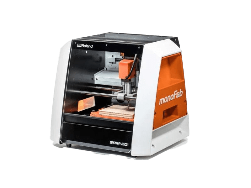
Roland SRM-20
The tool used for cutting the boards is the Roland SRM-20. Is a compact CNC desktop milling machine used for prototyping, PCB milling, and small mechanical parts. It removes material using rotating cutting tools.
Work area: 203.2 × 152.4 × 60.5 mm
Table size: 232.2 × 156.6 mm
Spindle speed: 3,000 – 7,000 rpm
Feed rate: 6 – 1800 mm/min
Mechanical resolution: ~0.000998 mm/step
Max workpiece weight: 2 kg
Control interface: USB (RML-1 or NC code)
Soldering
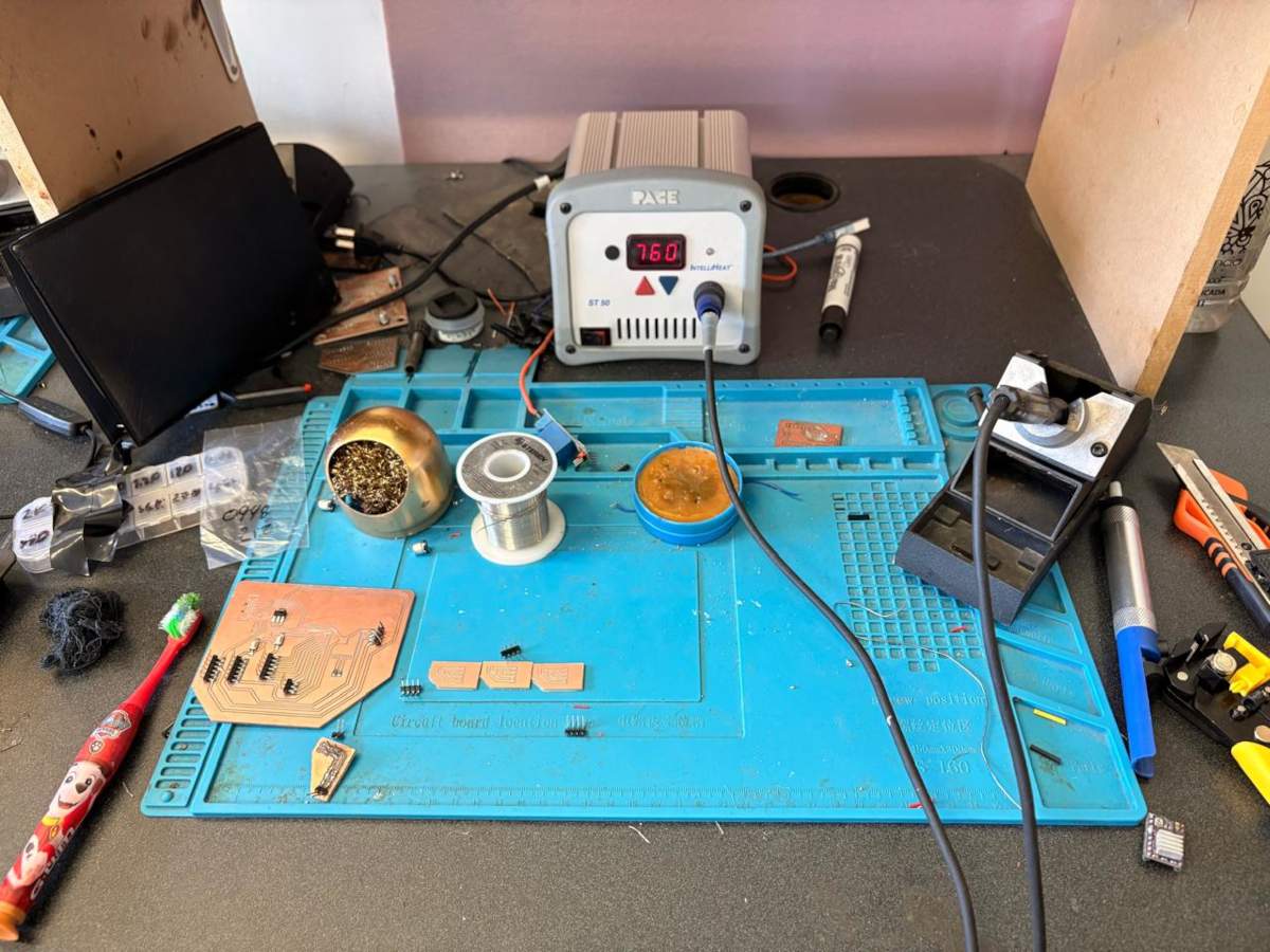
1. To solder, we first need to set up our workspace and gather the necessary tools.
Necessary tools
- Soldering station
- Flux
- Soldering Tin
- Desoldering mesh
- Silicone Tablecloth
Components
- Pinheaders
- 3 10μF smd Capacitors
- 4 100nF smd Capacitors
- 1 AMS1117
- 1 USB TYPE A
- 39 Pinheaders
- 1 ESP32 WROOM 32
- 2 Buttons
- 2 0 resistors
- 1 10k resistor
- 1 2k resistor
- 6 1M resistors
- 1 LED
Soldering
2. First, we need to apply flux to our PCB so that the solder adheres better.
3. Then, we have to turn on the soldering station and set the temperature. To solder tin it is recomendable to place the temperature above 300 °C (572 °F). I will use 404 °C (760 °F) because that works good with my materials.
4.To solder, we have to place the soldering iron over the copper board and heat it up, then we have to place the Tin on the surface and wait until it melts. It is important to place the Tin on the copper surfance and not on the soldering iron because the melted Tin flows toward hot surfaces, if we place it on the soldering iron, it won't adhere easily to the copper surface because it will be cooler.
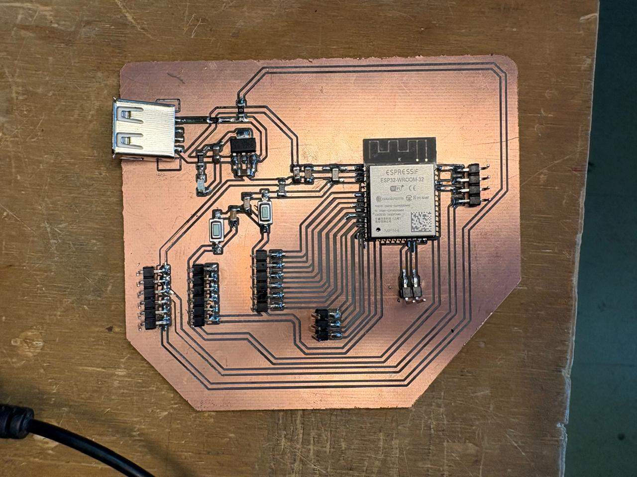
Results
Main board
Step Response
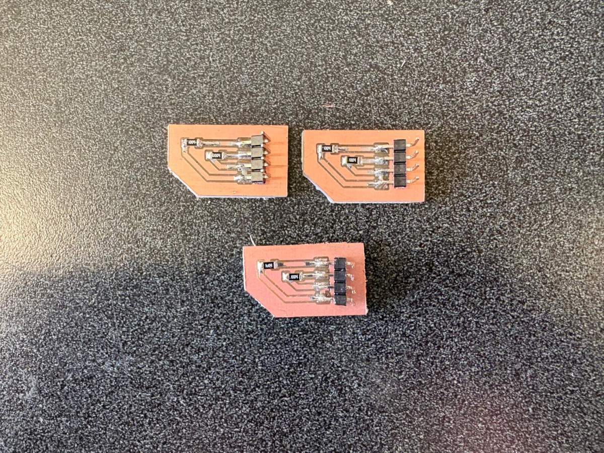
Step Response
Part Design
NEOPIXELS case
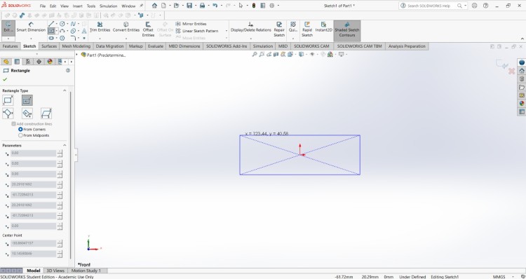
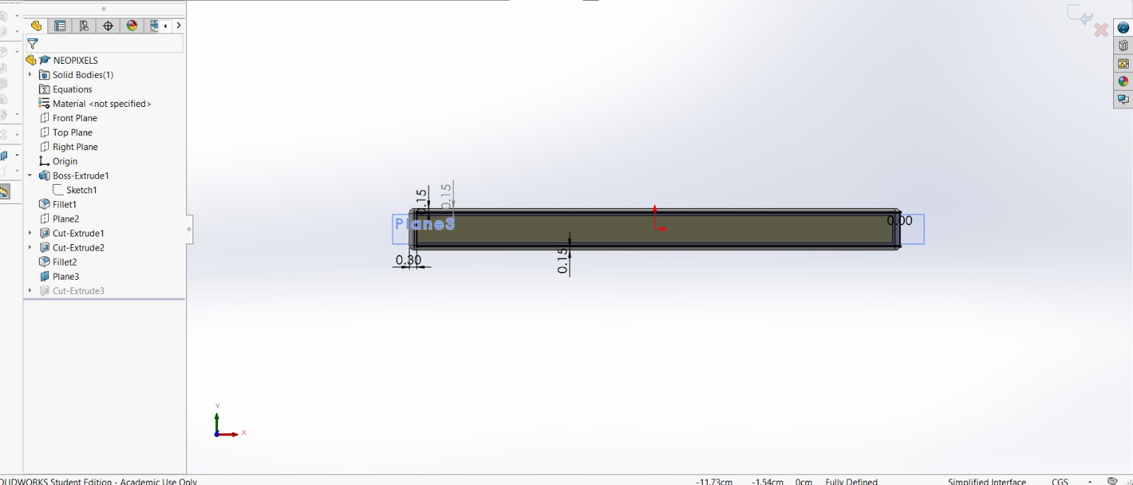
1. First, I changed the document units to CGS and created a center point rectange of 1.7 X 20 cmin the front plane.
NEOPIXELS case
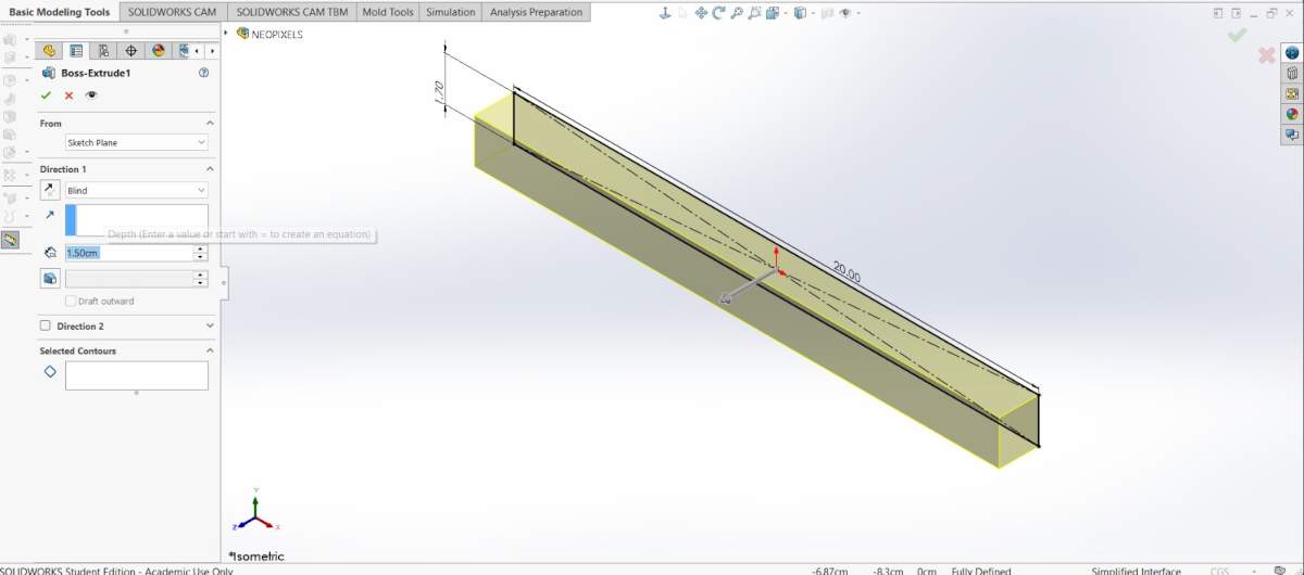
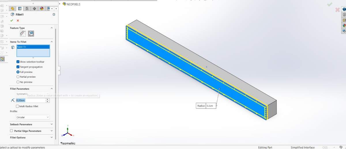
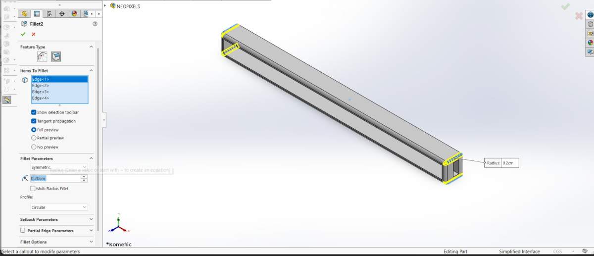
2. Then, I extruded it 1.5 cm and made roundings of 0.20 cm.
NEOPIXELS case
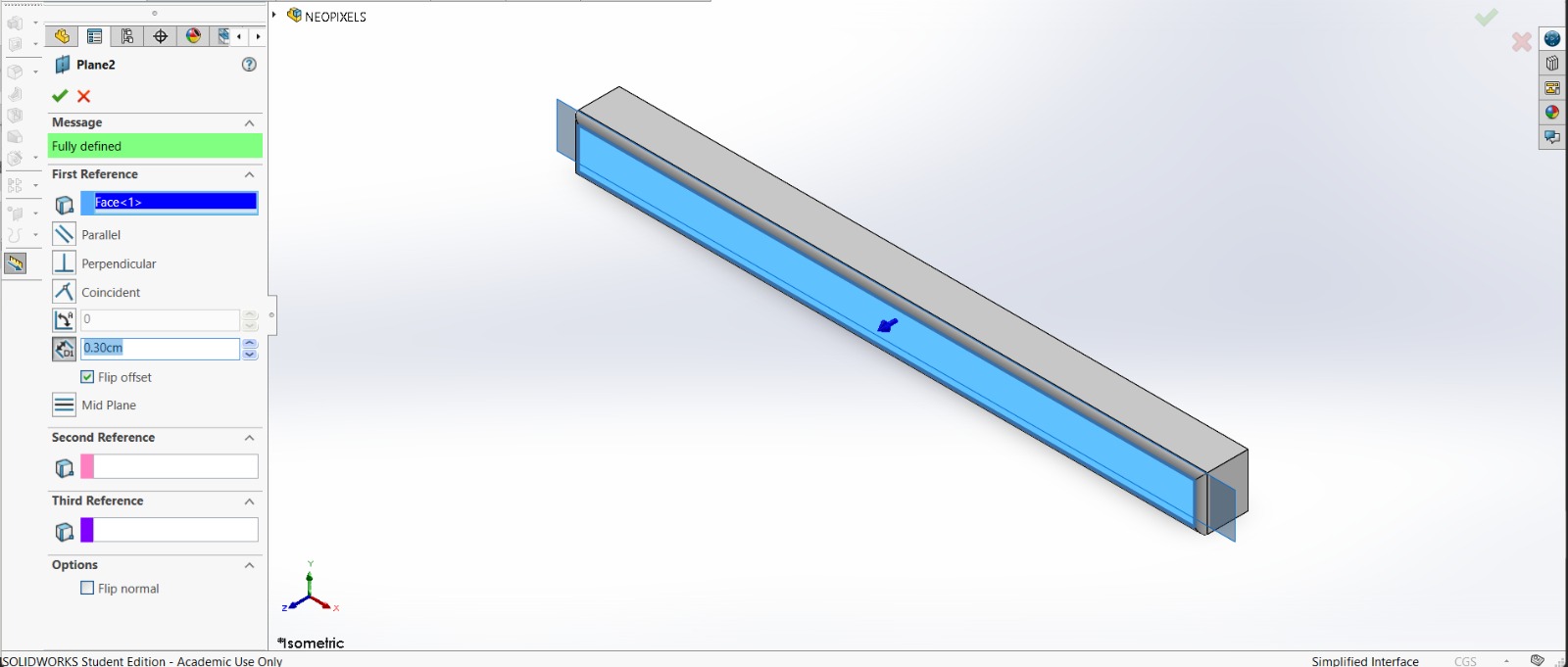
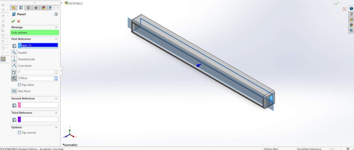
3. After that, I made a plane 0.30 cm from the front face of the piece.
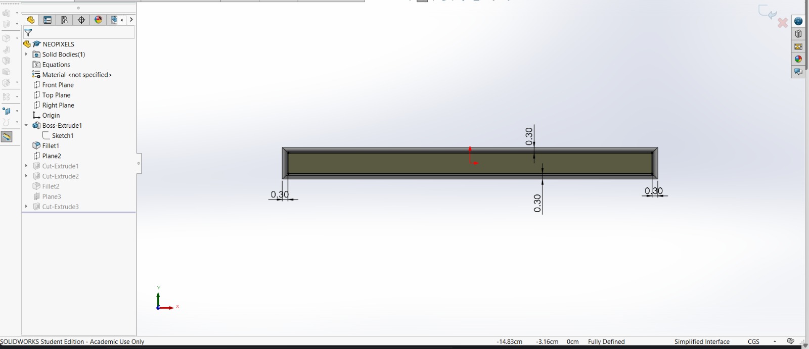
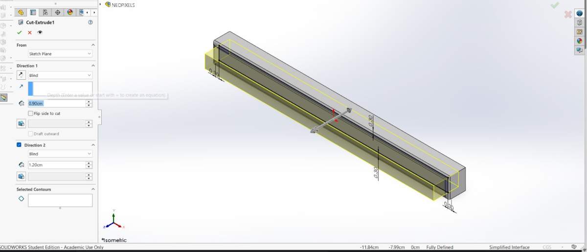
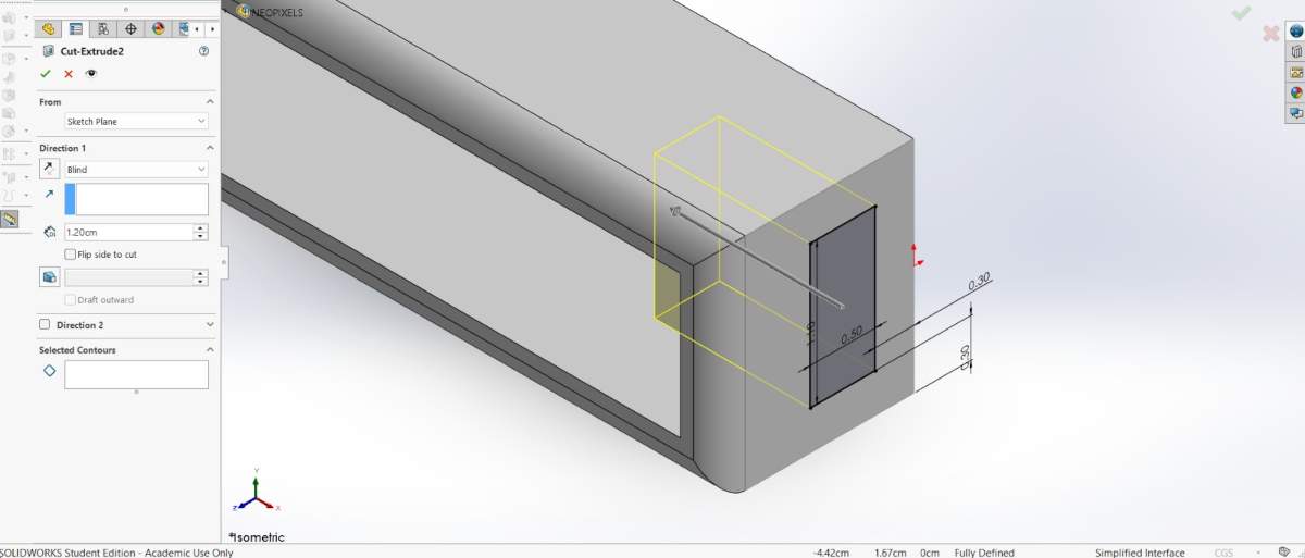
4. And in that plane made a rectangle with a distance of 0.30 cm from each edge. Then, I extruded a cut of 0.90 cm inside.
NEOPIXELS case
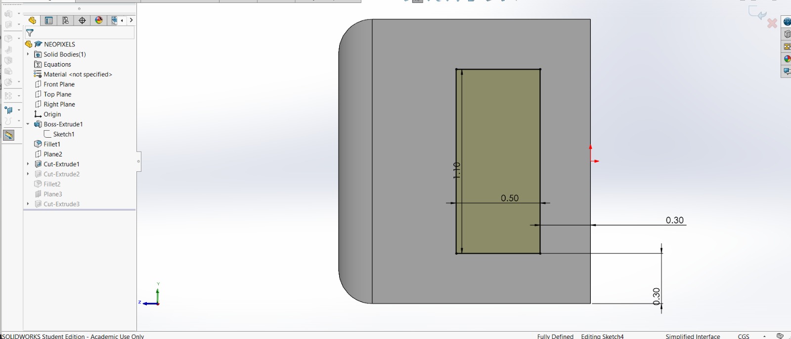
5. Subsequently, in the lateral face of the piece I made a rectangle of 1.10 X 0.50 cm at a distance of 0.30 cm from each edge. Next, I extruded a cut inside. I also added roundings in the corners so it could look better.
NEOPIXELS case
6. After that, I made a plane 0.90 cm from the back face of the piece.
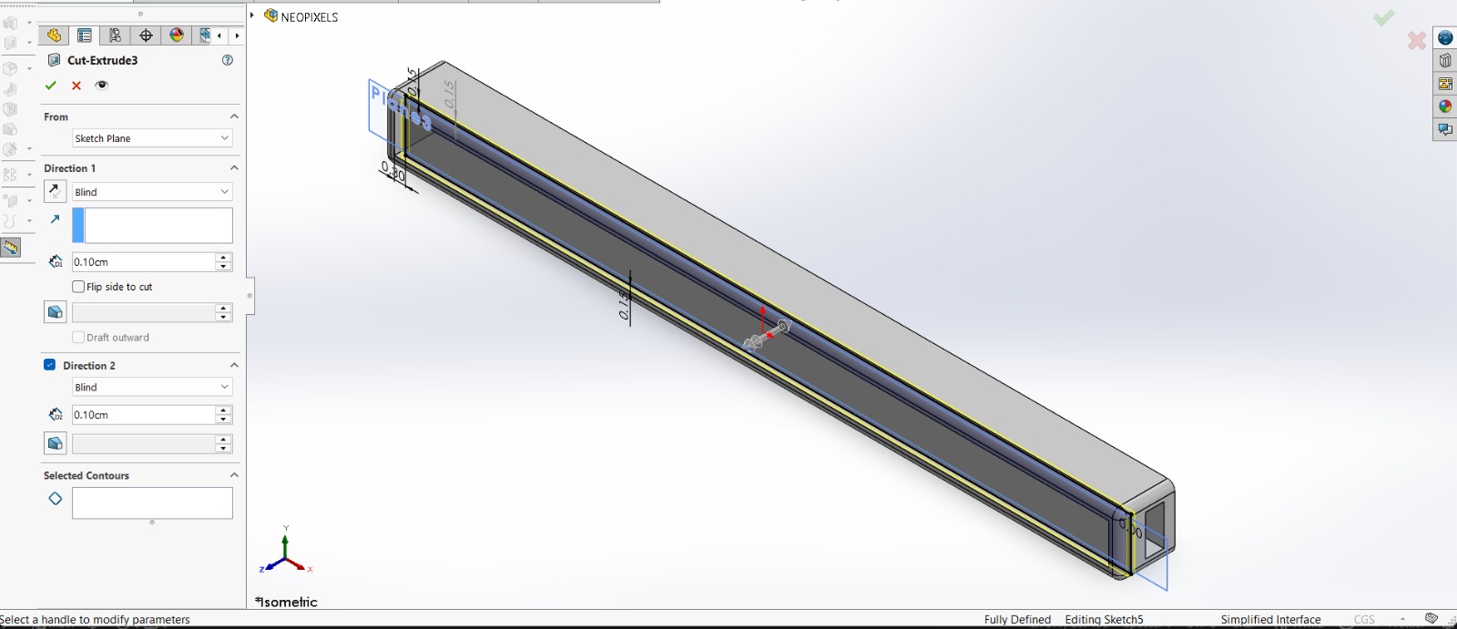
7. Then I added a rectangle to create a tab where I could later insert a transparent sheet. Then, I extruded a cut of 0.10 cm inside and outside.
Results
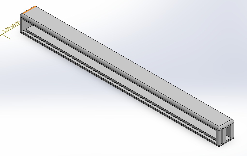
Export. We have to export our piece as an STL so we can print it. For that, we must go to File, then look for Save as and save it as STL.
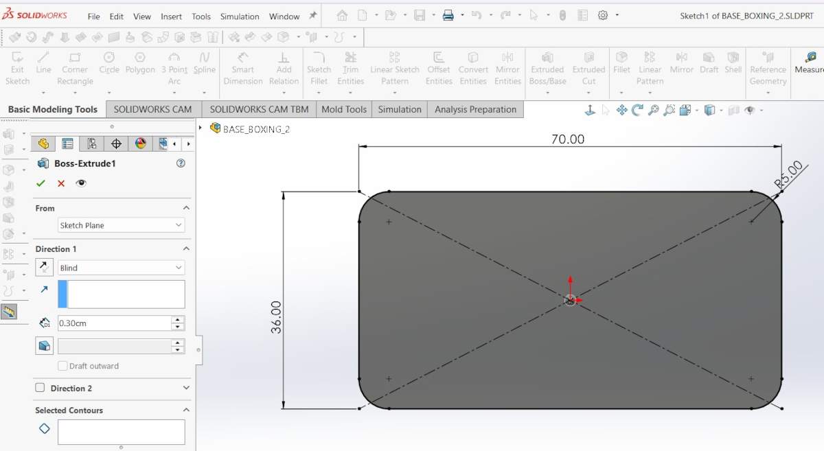
ESP32 case
1. First, I should have changed the document units to CGS, but I forgot, so it will be in MMGS. The I created a center point rectange of 110 X 100 mmin the front plane.
ESP32 case
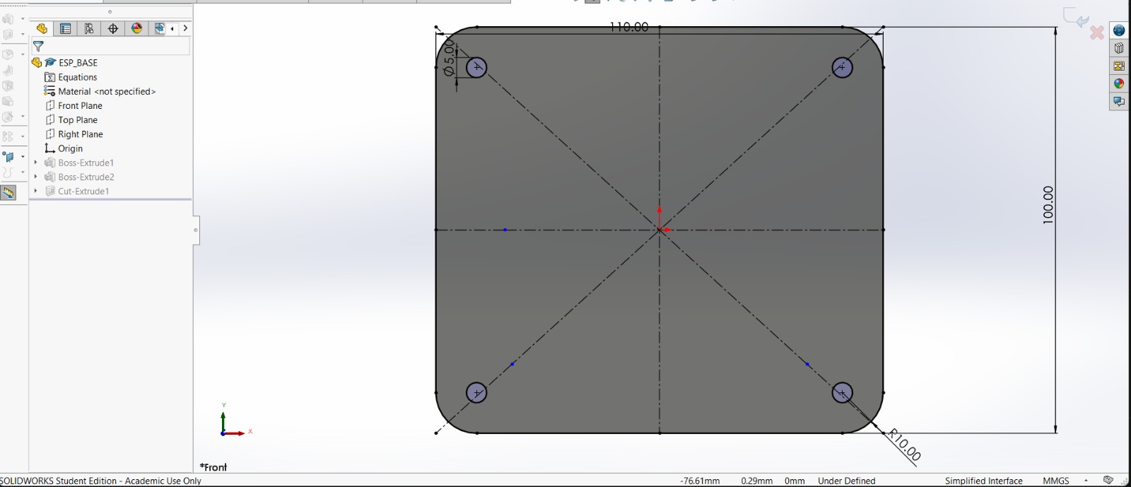
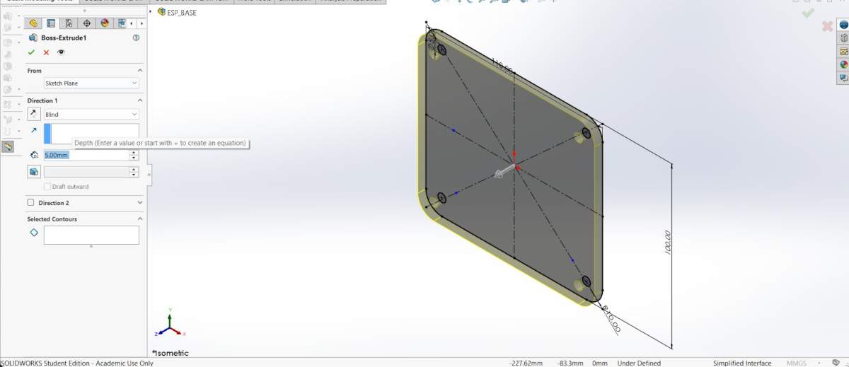
2. Then, I made round corners of 10 mm of radius and tiny holes of 5 mm of radius for screws. Next, extruded it 5 mm.
ESP32 case
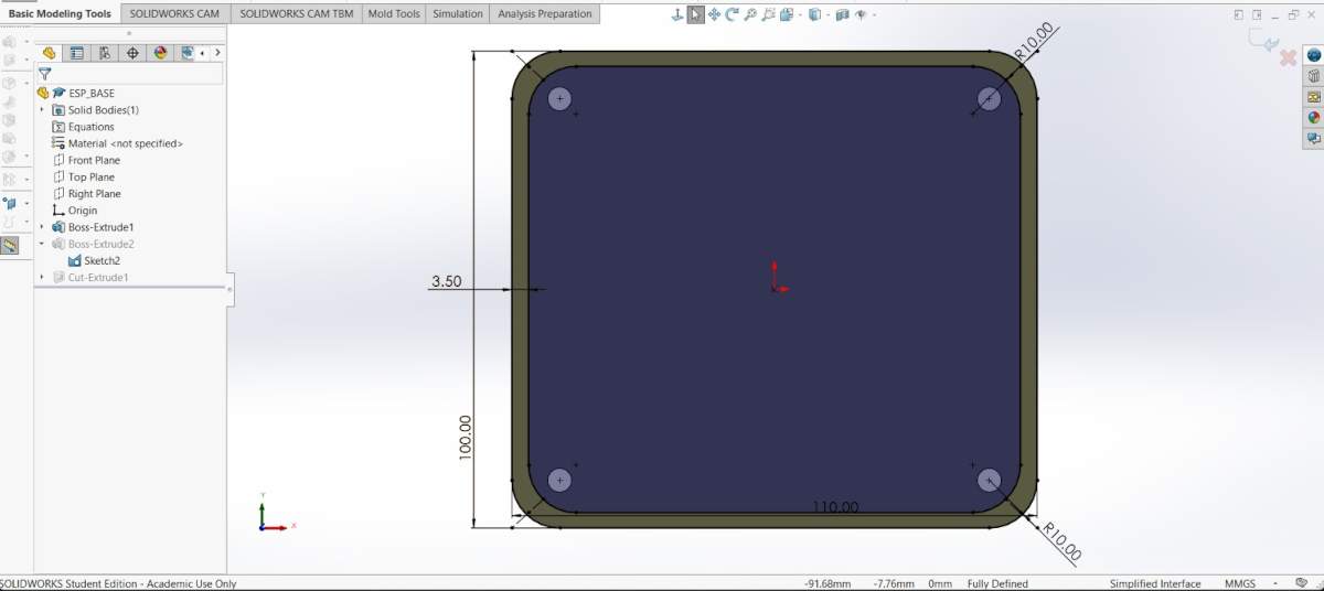
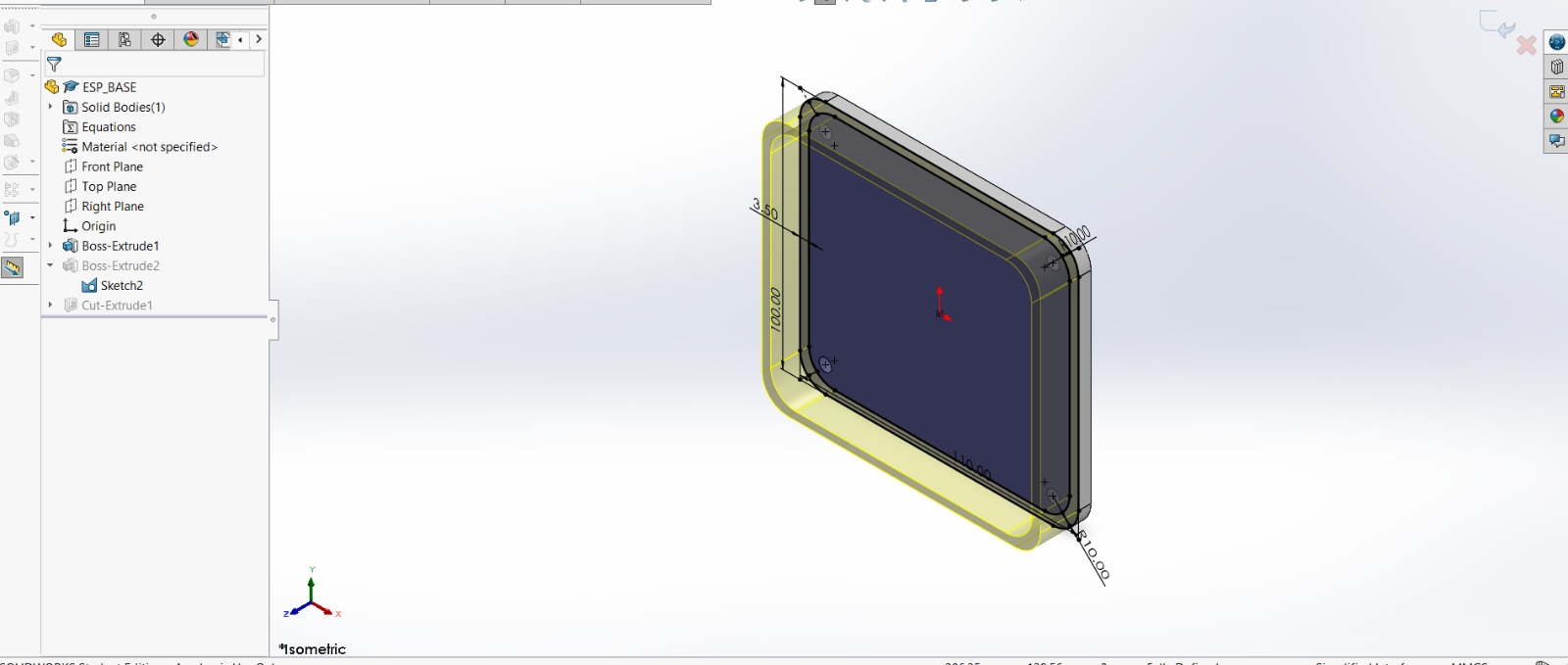
3. Then, I made the same figure inside, but with a distance of 3.5 mm from each edge. After that, I extruded it 15 mm.
ESP32 case
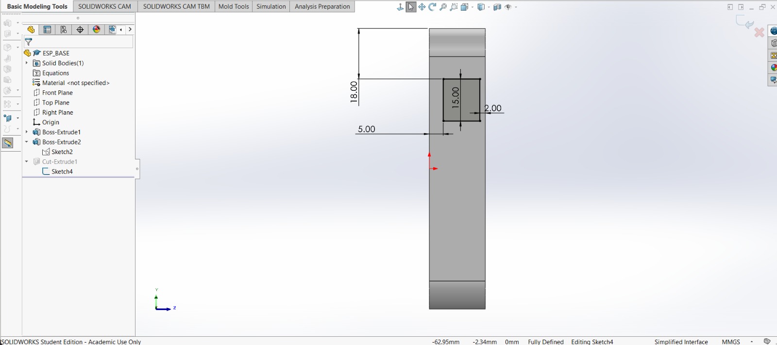
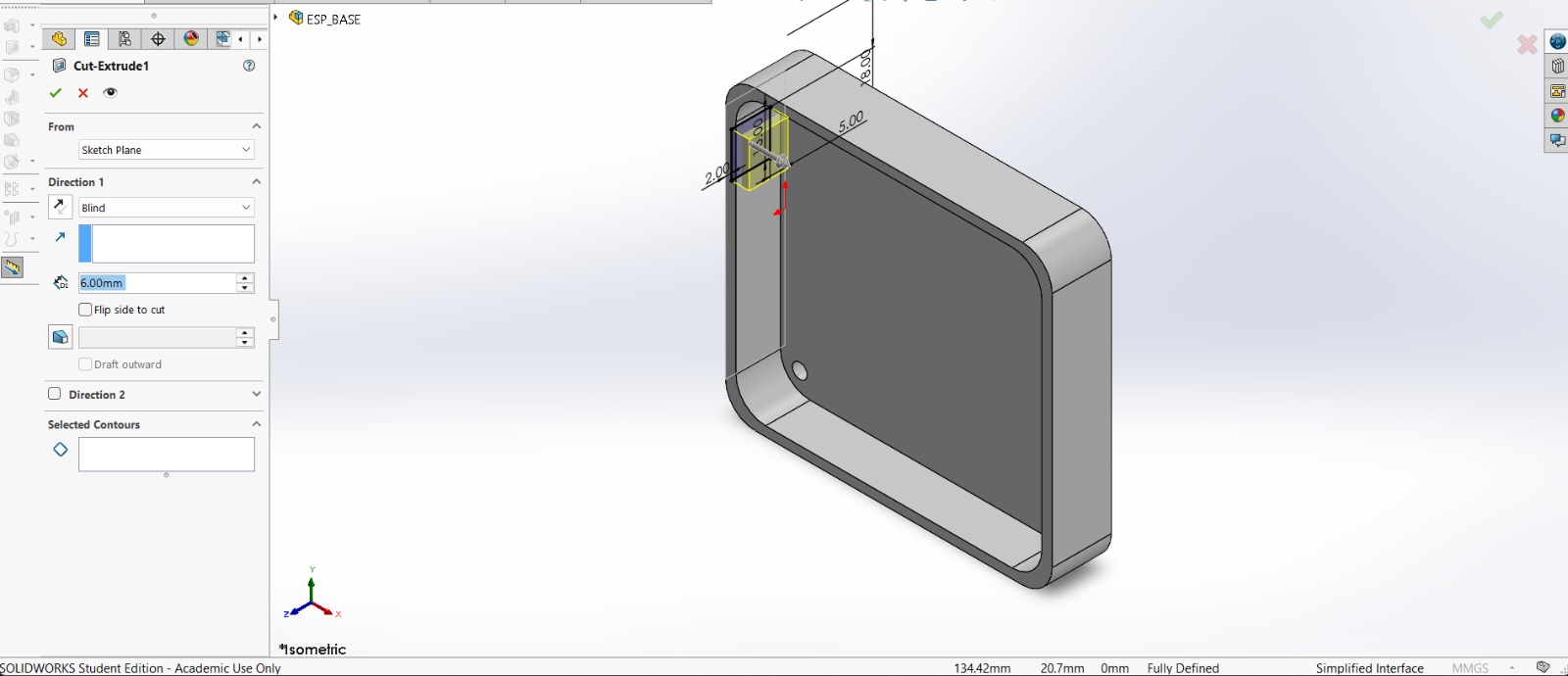
4. Subsequently, in the lateral face of the piece I made a rectangle of 13 X 15 mm at a distance of 18 mm from the top. Next, I extruded a cut inside.
Results
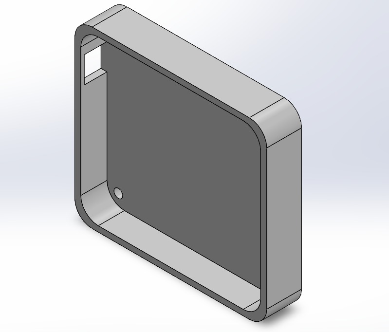
Export. We have to export our piece as an STL so we can print it. For that, we must go to File, then look for Save as and save it as STL.
Results
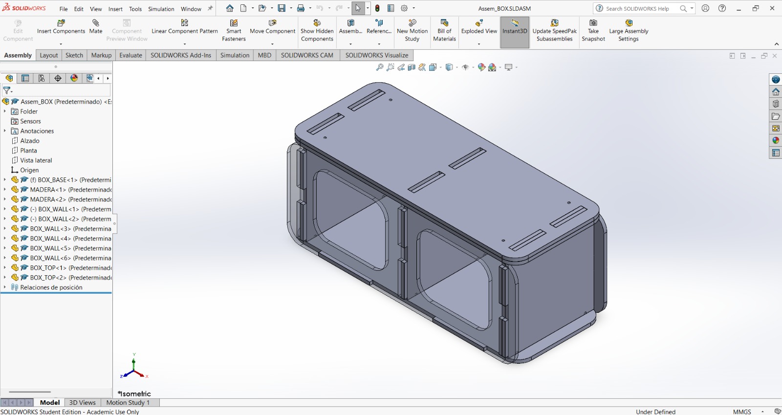
RESULTS.I made an Assembly with all the pieces to make sure everything was correct.
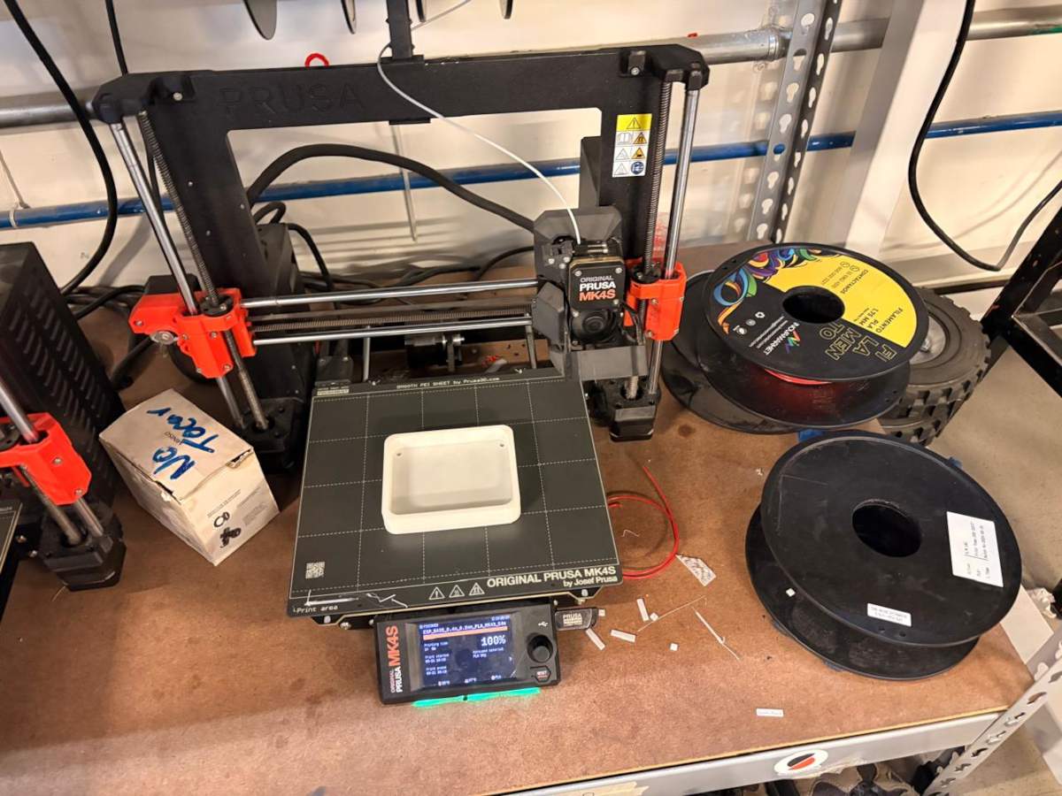
Part Printing
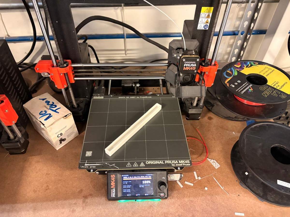
Printing
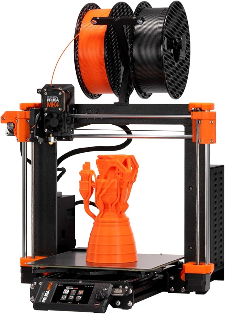
To print, I used Prusa Slicer. I will also use a Prusa MK4S for the 3D printing process.
NEOPIXELS case
1. First, open the slicer. and import the STL piece.
NEOPIXELS case
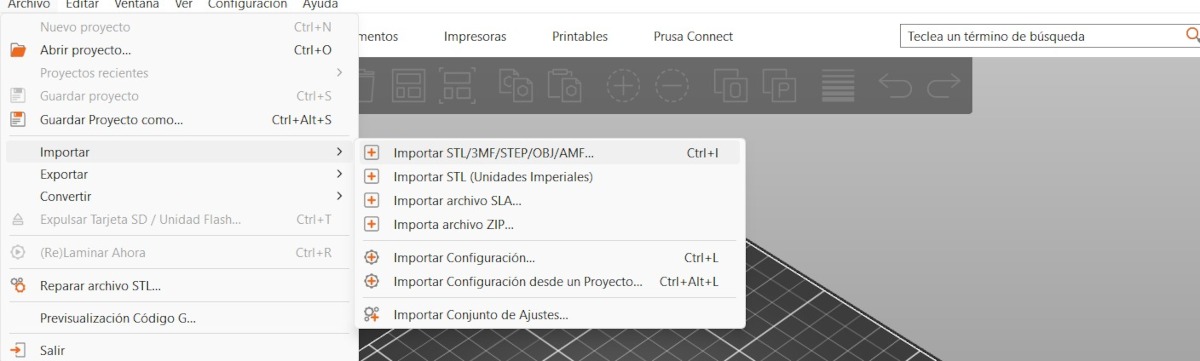
2. For importing, we have to press File, then import and select import STL.
NEOPIXELS case
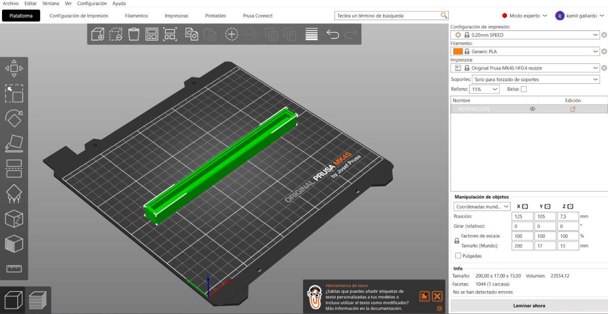
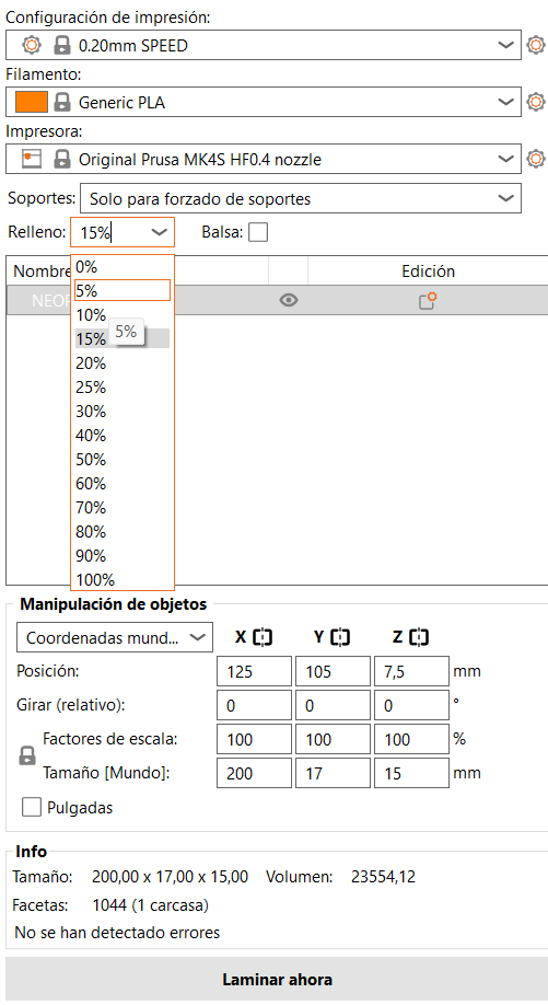
3. After that, we have to set the printing parameters. Being honest, I just placed my piece on the center, changed the material to PLA and also changed the infill to 5%.
4. Then, we just have to press the button at the buttom labeled as SLICE.
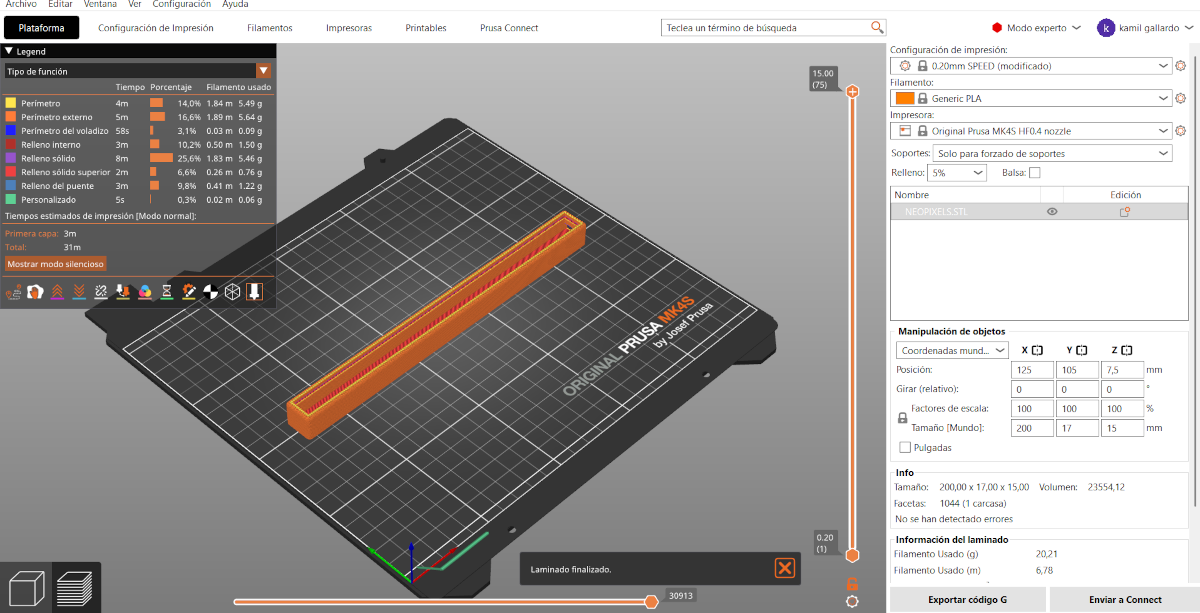
5. Having sliced our piece, we can see the way it will be printed and, by pressing the button below, we can save it in the prusa USB.
Results
ESP32 case
1. First, open the slicer. and import the STL piece.
ESP32 case
2. For importing, we have to press File, then import and select import STL.
ESP32 case
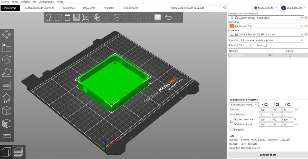
3. After that, we have to set the printing parameters. Being honest, I just placed my piece on the center, changed the material to PLA and also changed the infill to 5%.
4. Then, we just have to press the button at the buttom labeled as SLICE.
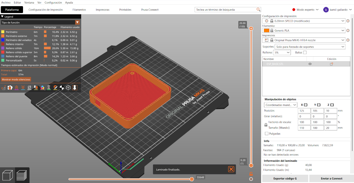
5. Having sliced our piece, we can see the way it will be printed and, by pressing the button below, we can save it in the prusa USB.
Results
Results
RESULTS.I made an Assembly with all the pieces to make sure everything was correct.
System Integration
Position footprint
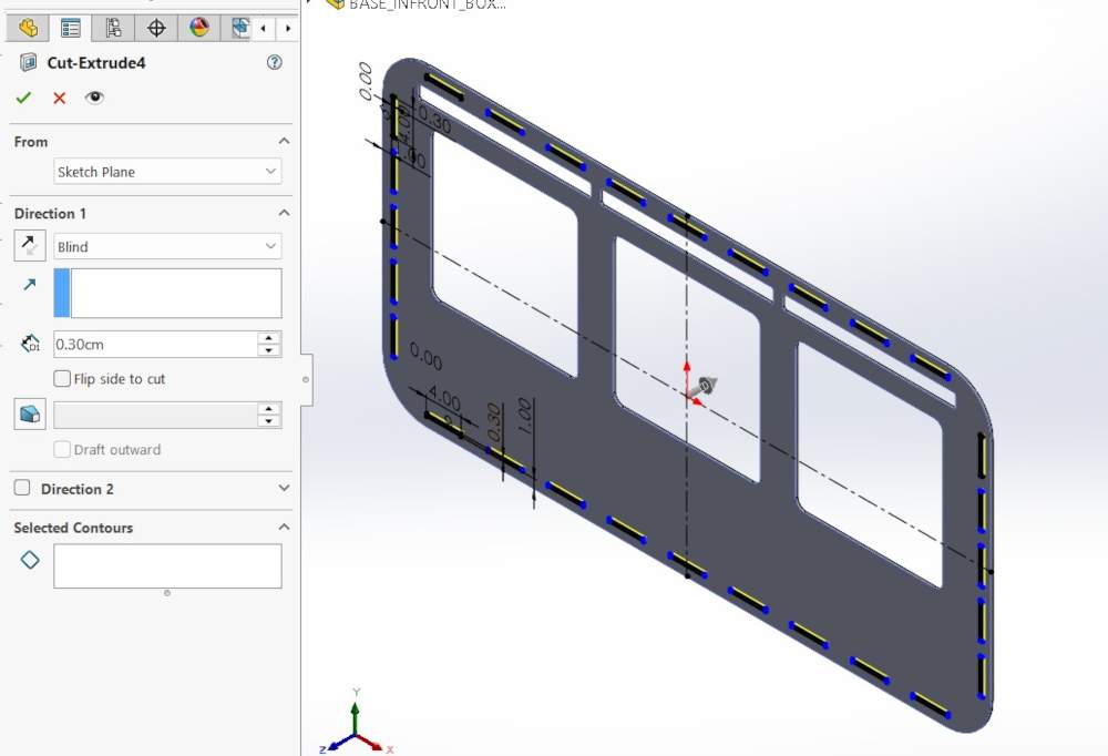
1. First, I changed the document units to CGS and created a center point rectange of 70 X 36 cmin the front plane.
Position footprint
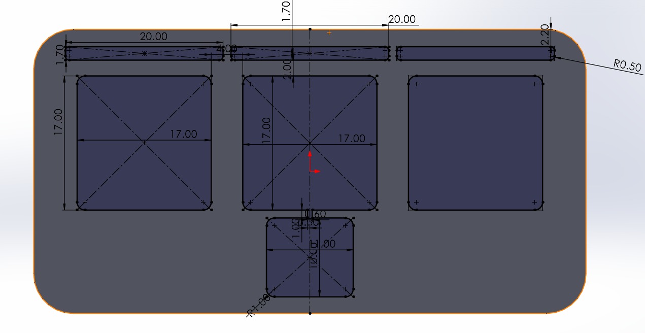
2. Then, I made fillets of 5 cm of diameter and extruded it 3 mm.
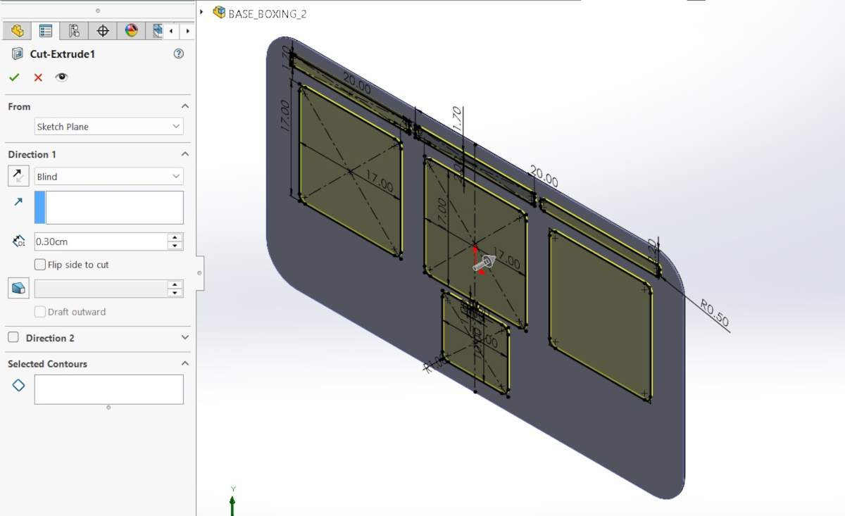
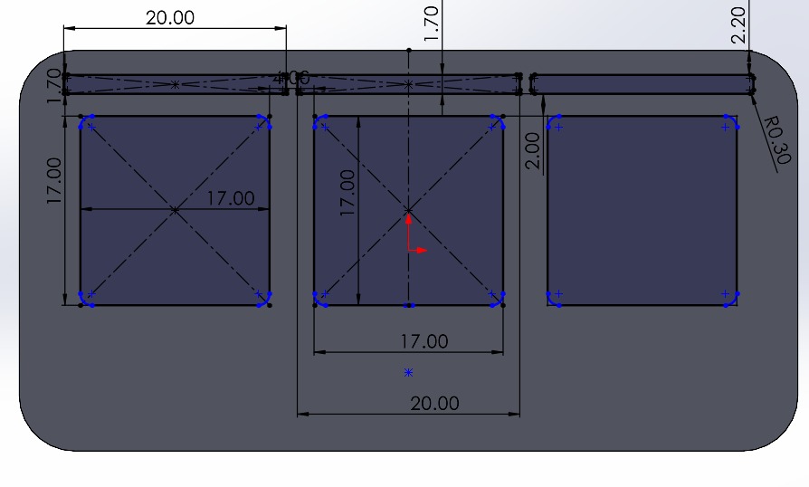
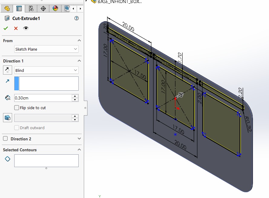
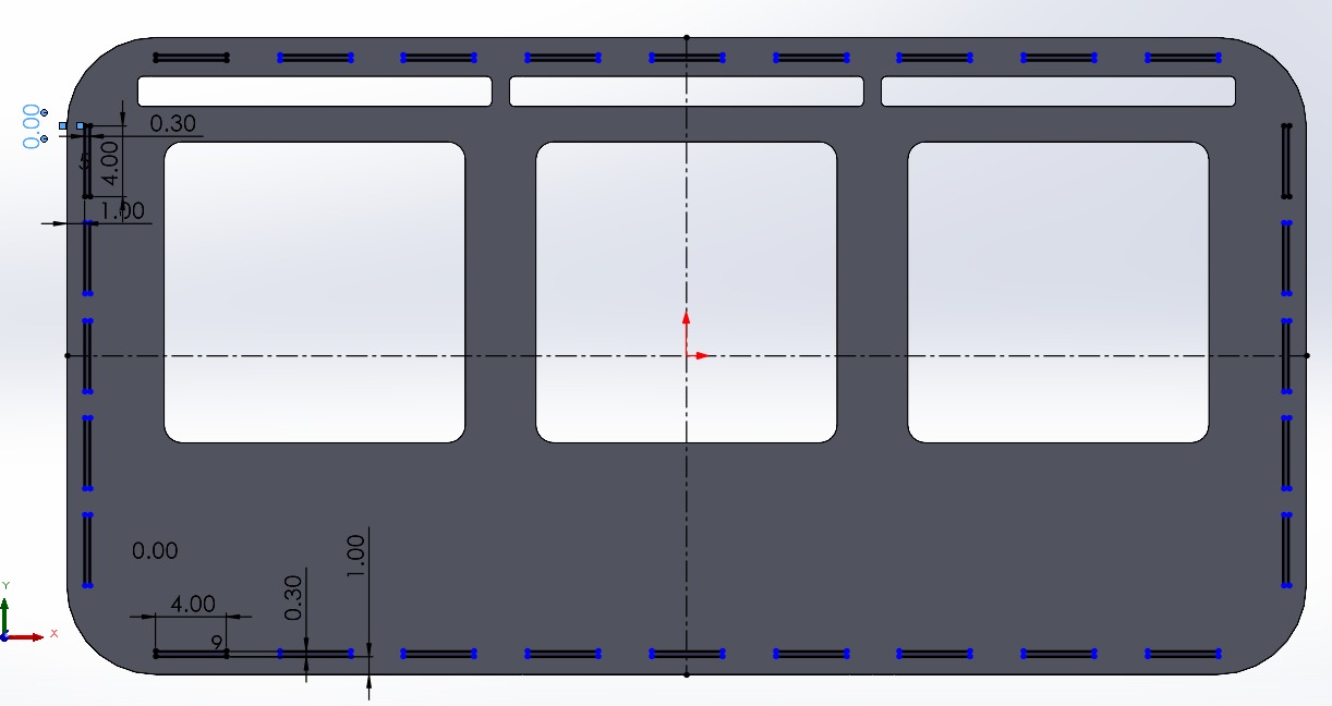
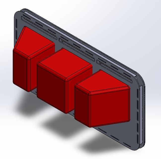
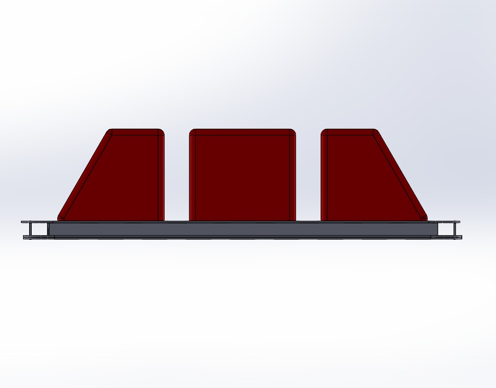
3. Next, I traced the outlines of the parts I’ll be placing in the assembly, which are: 3 Neopixel casings, 3 pads, and the ESP32 casing. My pads will measure 17 x 17 cm, spaced 4 cm apart, with a 2 cm distance from their respective Neopixels and a 1 cm vertical distance from the center pad to the ESP32 housing. Then I extruded the cut.
Position footprint
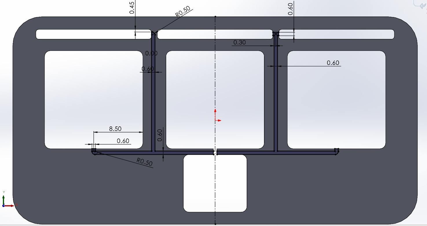
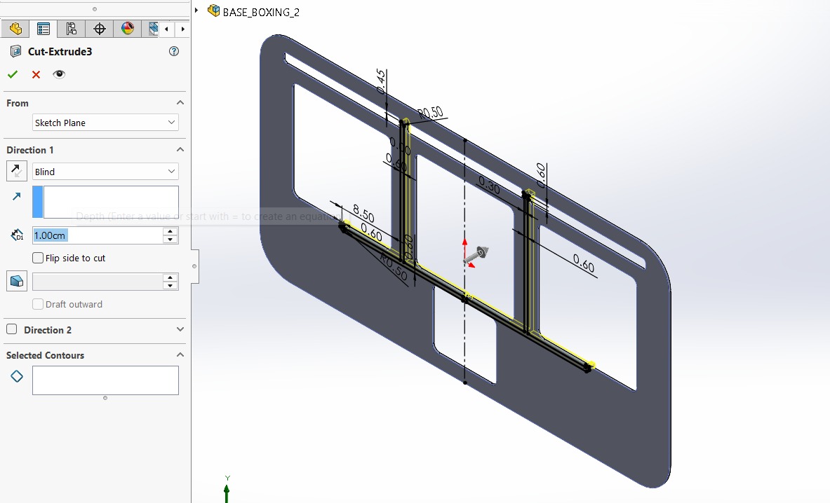
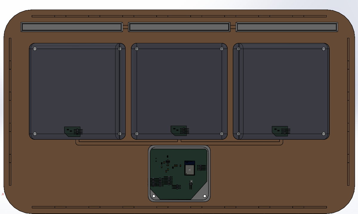
4. After that, I made small conduits of 6 mmto keep the wires from my components tidy. They all go to the ESP32. I made sure the wires from the pads were shorter so as not to interfere with the signal from my sensors. Subsequently I extruded a cut.
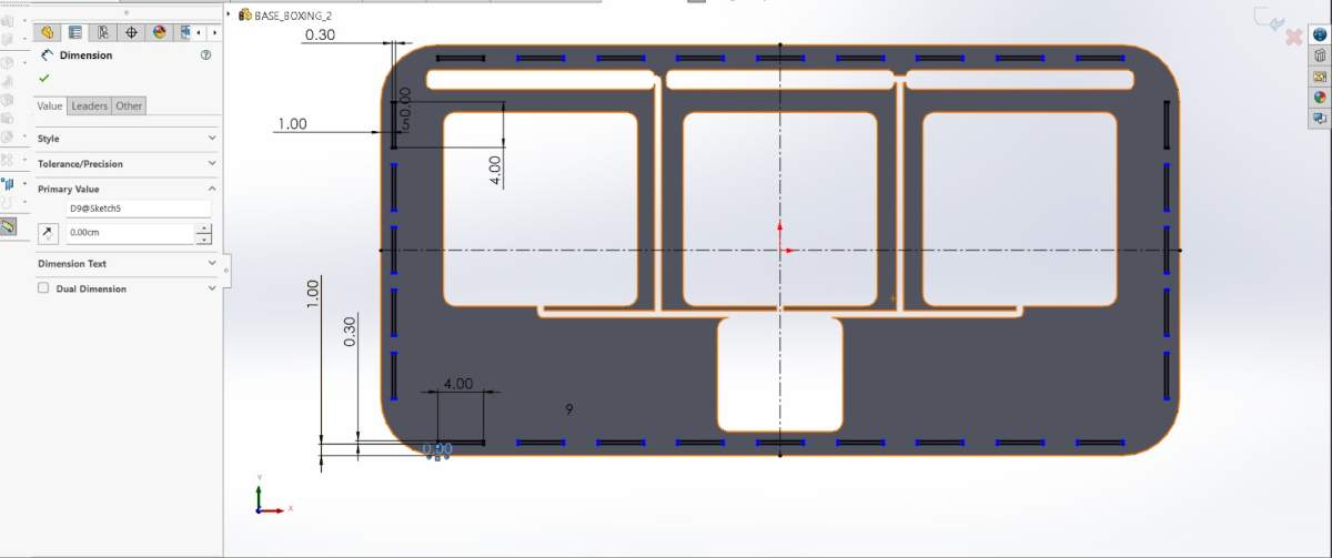
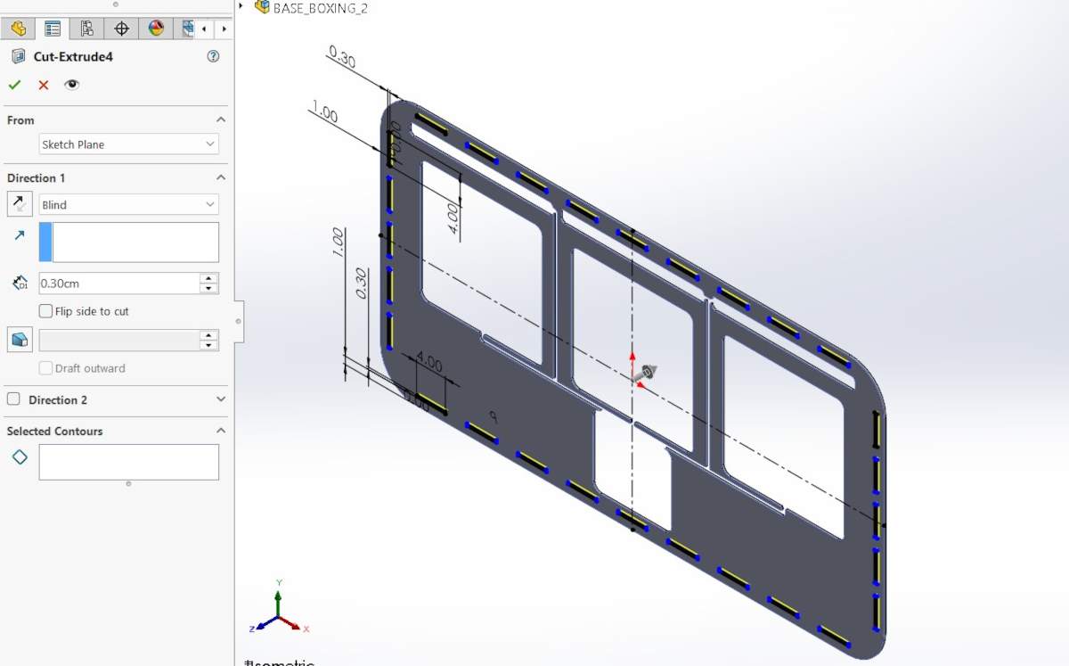
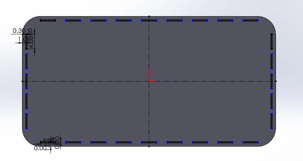
5. Finally, I mide small joints around mi piece. These joints are used to attach walls so I can place a panel on top to hide my circuit board and the wires. There are 5 on the sides, and 9 on the top and bottom. They measure 0.3 x 4 cm. Then, as usual, I extruded another cut.
Base
1. First, I changed the document units to CGS and created a center point rectange of 70 X 36 cmin the front plane.
Base
2. Then, I made fillets of 5 cm of diameter and extruded it 3 mm.
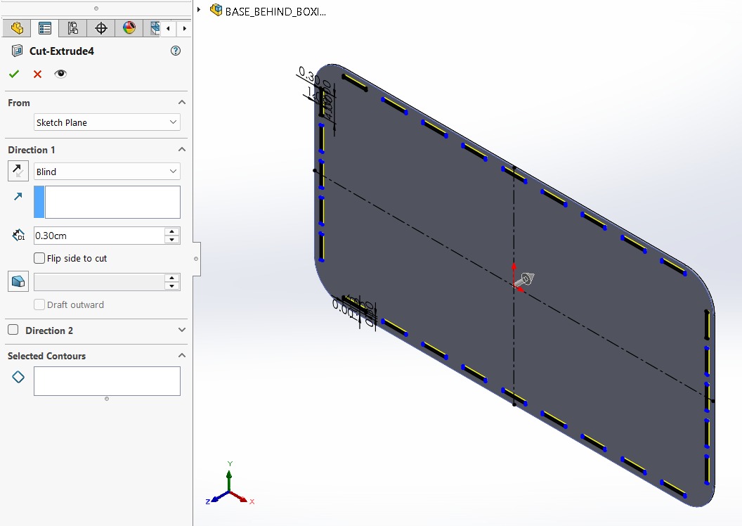
3.After, I made small joints around mi piece. The same I did the piece before. This will serve as the base that supports everything, the previous layer will be placed on top of it, and the walls will be built on top of those two layers before the main facade is installed.
Base
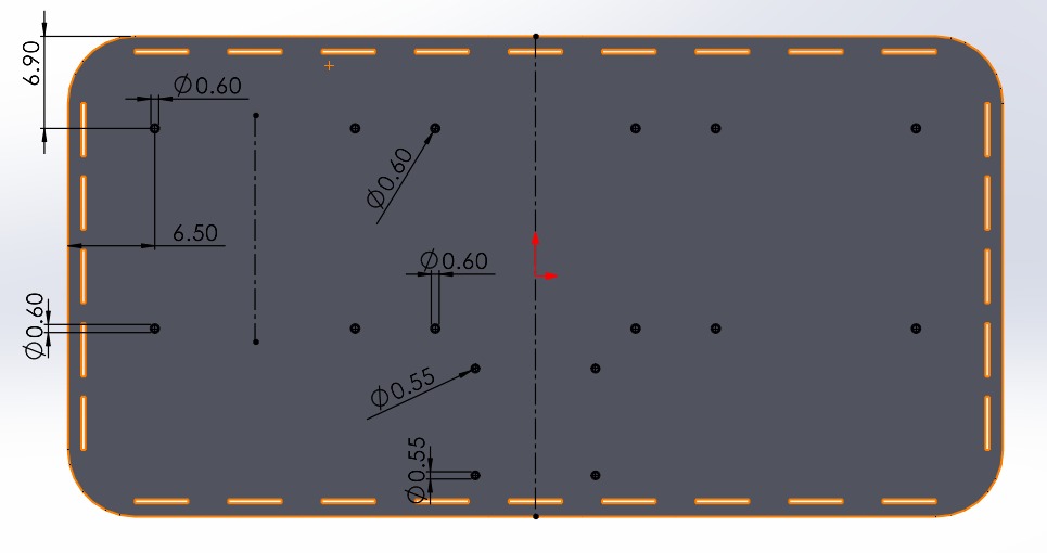
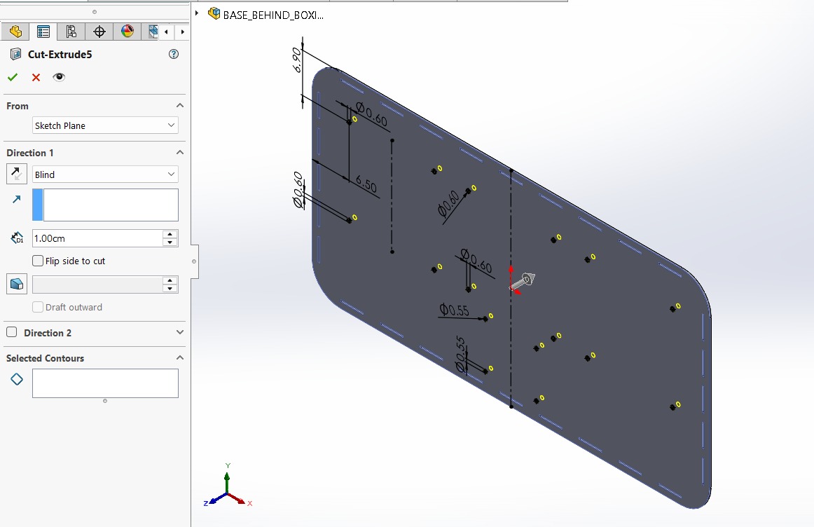
4. Next, following the measurements I had already taken, I drilled holes to accommodate the screws. The top ones are positioned at the edge of the pads and are M6. The bottom ones are for the ESP32 and are M5.
Pad Base
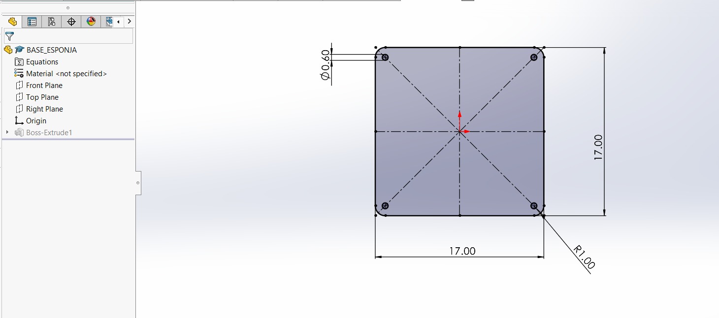
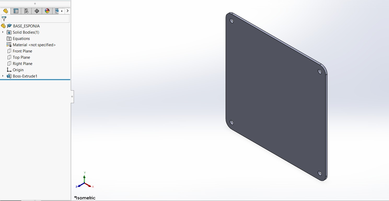
5. Also create the bases for the pads; this is to provide them with better support. They measure 17 x 17 cm, with a 1-cm fillet, and have the same 6-mm holes 1 cm from the side and top edges.
Walls
1. First, I changed the document units to CGS and created a center point rectange of 70 X 36 cmin the front plane.
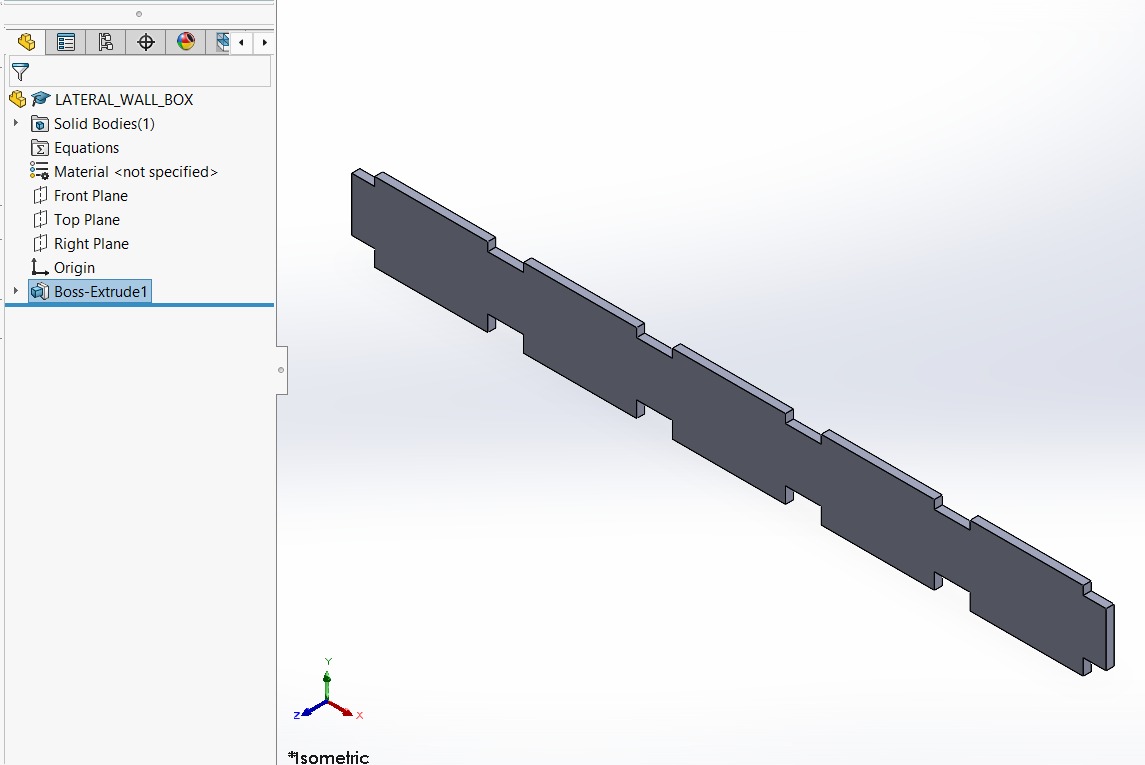
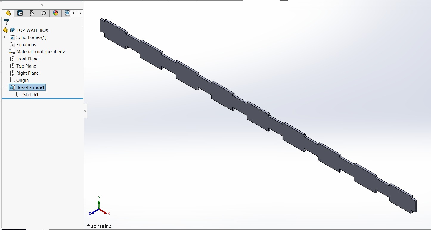
Walls - lateral
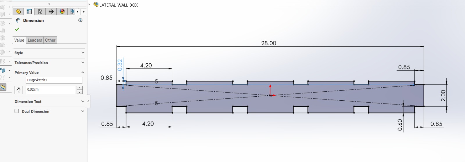
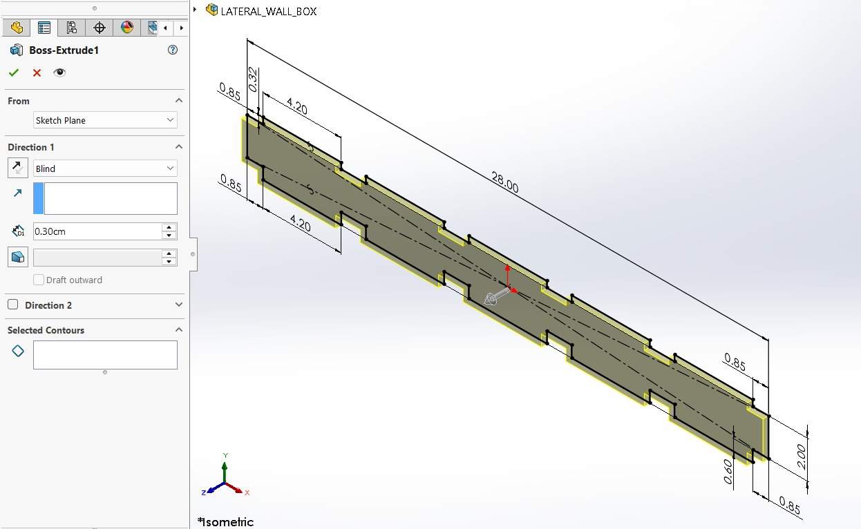
Lateral Wall. The lateral wall design consists of 5 teeth at the top and bottom. The top teeth measure 4.2 × 0.3 cm and the bottom teeth 4.2 × 0.6 cm, taking into account the kerf and the fact that the bottom must fit into two layers 0.3 cm thick. I then extruded it by 0.3 cm.
Walls - Top and Bottom
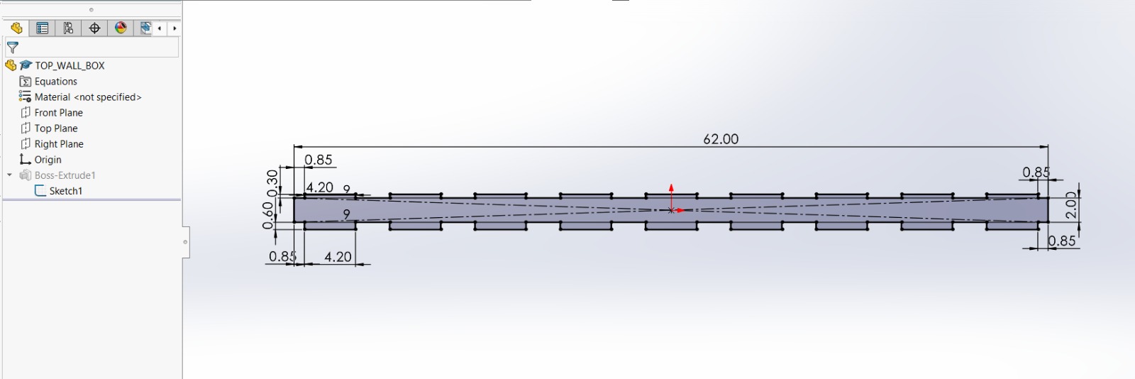
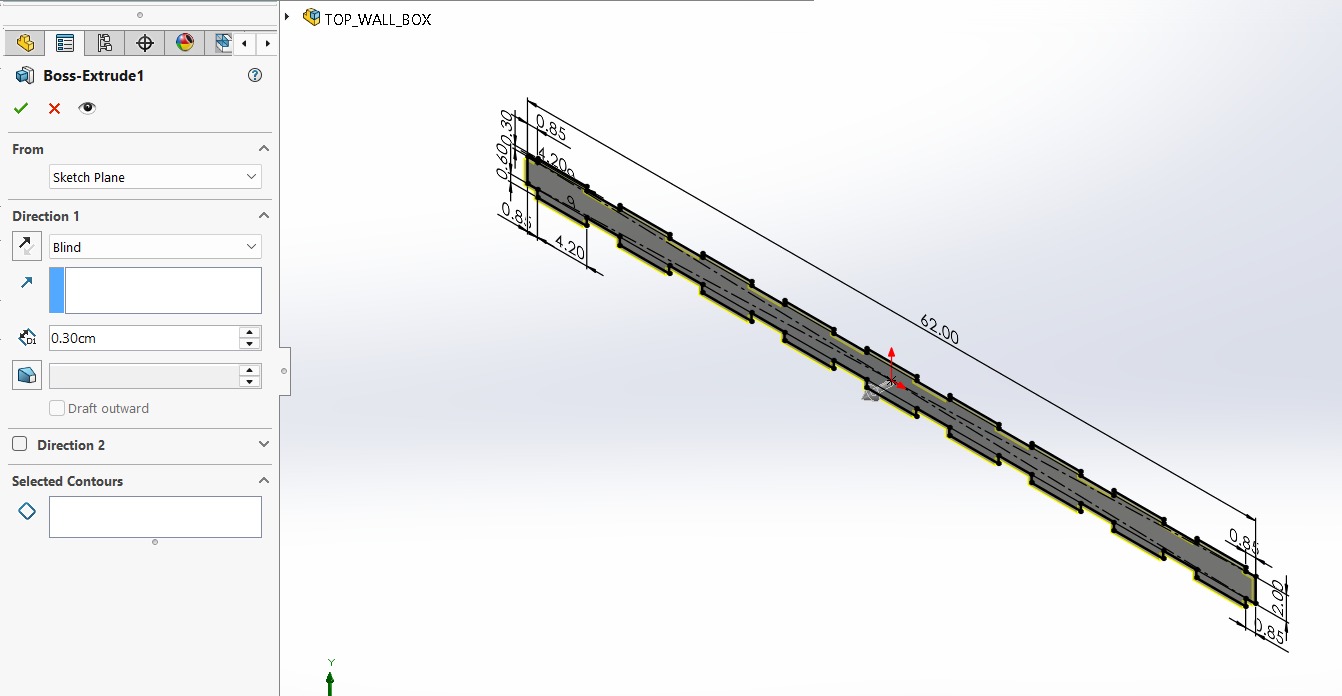
Top and Bottom Wall. The design of the top and bottom walls consists of 9 teeth on each side. The top teeth measure 4.2 x 0.3 cm and the bottom teeth measure 4.2 x 0.6 cm, taking into account the kerf and the fact that the bottom section must fit into two layers, each 0.3 cm thick. I then extruded it by 0.3 cm.
Walls
Front Face
1. First, I changed the document units to CGS and created a center point rectange of 70 X 36 cmin the front plane.
Front Face
2. Then, I made fillets of 5 cm of diameter and extruded it 3 mm.
3. Next, I traced the outlines of the parts I’ll be placing in the assembly, which are: 3 Neopixel casings and 3 pads. My pads will measure 17 x 17 cm, spaced 4 cm apart, with a 2 cm distance from their respective Neopixels. I will leave the space below blank because I want to cover the wires and the esp32.
Front Face
4. After that, I made the same holes for the joints I made in the Base an the Position Footprint.
Results
RESULTS.I made an Assembly with all the pieces to make sure everything was correct.
Cables
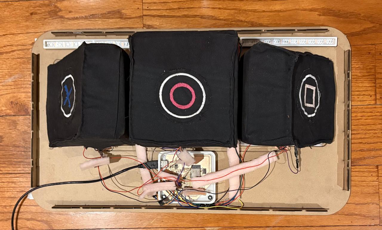
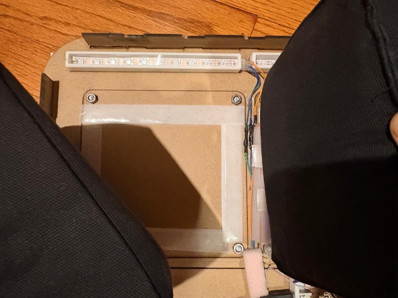
Cables.To route the wires, I had created a 3D model of my circuit boards to get an idea of how I was going to arrange them. Unfortunately, as the project progressed, I realized there was a lot of noise affecting my sensor readings, so I had to use some foam to space the wires apart and minimize the noise as much as possible; however, this solution didn’t give me a very clean result.
Attaching
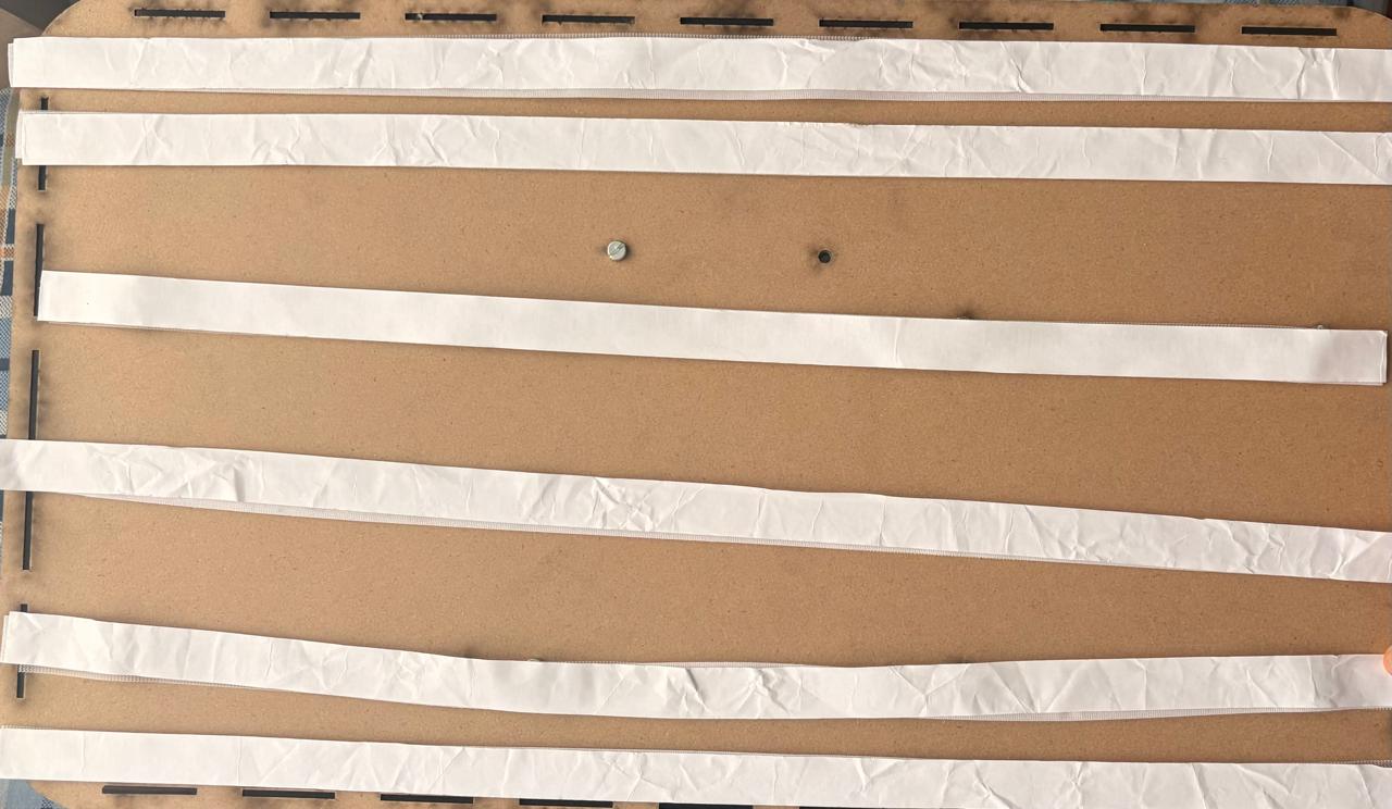
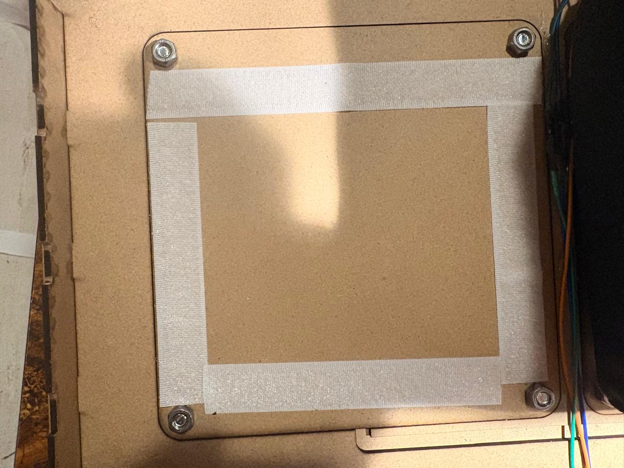
Attaching.To attach my pads, I cut the adhesive Velcro I had and placed it on the back of the pads, then attached the other side of the Velcro to the pads themselves. The result surprised me—it held quite firmly thanks to the excellent adhesive on the Velcro. I also used it to attach B.R.I.S. to the wall, and it worked just as well; it stayed firmly in place.
Learning outcomes
This week I learned a lot about project assembly and system integration. At first, I was unsure of how all the components would fit together, and the process seemed more challenging than I had expected. Once I began assembling the project, I decided to create dedicated channels for the cables and add markings to indicate the position of each component. This approach not only improved the overall organization of the system but also made it much easier to understand how everything connects. Additionally, if the project ever needs to be disassembled for storage or transportation, these markings will provide a clear guide for reassembly.
Regarding the pads, I found that their current size is appropriate because they provide a large enough target area for accurate hits while also allowing the electronics to remain compact. Keeping the pads relatively close together helps minimize cable lengths, which can reduce signal degradation and improve reliability. As for packaging, I concluded that shipping or storing the system fully assembled would be the most practical solution. Packaging each component separately would make the process much more time-consuming and could increase the risk of losing parts or making reassembly more difficult for the user. Overall, this week helped me better understand the importance of planning not only the design of a project but also its assembly, maintenance, and usability.