Week 11: Networking and Communications
This week, we explored networking and communications, focusing on the various protocols microcontrollers use to exchange data, whether sending commands or sharing process information. As part of the assignment, we tested and compared different communication protocols, evaluating their effectiveness for wired and wireless applications. Click here to check on this week's group assignment page.
Work log
Completed tasks
- Demonstrated workflows used in network design.
- Implemented a communication protocol.
1.What is a communications protocol?
A communication protocol is a set of rules or an agreed-upon "language" that microcontrollers use to exchange data with each other reliably. It ensures that the data is sent, received, and understood correctly between devices.
Why are communication protocols necessary? Microcontrollers are capable but limited devices; they have finite processing power, memory, GPIO pins, and peripherals. When a system grows in complexity, a single microcontroller often can't handle everything efficiently. This is where inter-MCU communication becomes essential.
Main reasons for offloading tasks to secondary microcontroller:
- Processing limits: When a primary MCU is tasked with motor control, sensor fusion, and display management simultaneously, it may struggle to meet real-time deadlines. Offloading time-critical tasks, such as motor PID loops, to a secondary microcontroller enables the main MCU to focus on higher-level logic and system coordination.
- Peripheral specialization: Different microcontrollers are optimized for specific functions. For example, an ESP32 excels at WiFi and BLE communication, an ATtiny is ideal for low-power I/O operations, and an STM32 is well-suited for precise timing tasks. Rather than using a single, potentially expensive MCU for all roles, deploying specialized microcontrollers can be more cost-effective and efficient.
- Real-time requirements: Tasks demanding strict timing—like PWM generation, encoder reading, or stepper motor control—benefit from being handled by a dedicated MCU. This approach prevents critical operations from being delayed by other processes running on the main controller.
- Physical separation: In distributed systems or robots, sensors and actuators may be physically distant from the main controller. Assigning local microcontrollers to handle processing at each node reduces wiring complexity, lowers latency, and increases system reliability.
- Power domains: A low-power microcontroller can remain active to monitor sensors or handle simple tasks while the main MCU enters a low-power sleep mode, thereby improving overall energy efficiency.
Common communications protocols include:
| Protocol | Wires | Topology | Speed | Typical Use |
|---|---|---|---|---|
| I2C | SDA, SCL | Multi-master / slave bus | 100 k – 3.4 M bps | Sensors, EEPROMs, MCU-to-MCU |
| SPI | MOSI, MISO, SCK, CS | Master / slave | 10s of Mbps | Displays, flash, fast sensors |
| UART | TX, RX | Point-to-point | Configurable | Debugging, GPS, MCU-to-MCU |
| CAN | CANH, CANL (differential) | Multi-node bus | Up to 1 Mbps | Automotive, robotics |
2. Which communication protocol did I choose to focus on for this assignment?
As I mentioned in my Week 9 assignment, I anticipated that I might revisit I2C at some point, and that time has come. For this assignment, I have decided to use I2C as the communication protocol. I have used I2C in the past; in my original robot, it served as the foundation for communication between my microcontrollers. For this new iteration of my robot, I require a similar type of connection, so I2C is once again the logical choice. Before I explain what I accomplished for this assignment, I'd like to provide a brief overview of the I2C communication protocol.
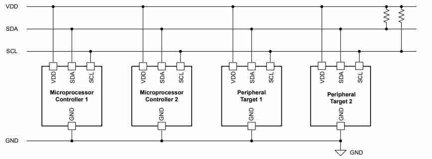
I2C (Inter-Integrated Circuit) is a synchronous serial communication protocol developed by Philips in the 1980s, designed for short-distance communication between integrated circuits (ICs) on the same board. It is widely used in embedded systems for connecting microcontrollers, sensors, and other peripherals. Before diving into technical details, it's important to understand that "short distance" in I2C typically means any length from a few centimeters up to about 1 meter. This limitation exists because I2C lines have inherent capacitance, and the I2C specification defines a maximum bus capacitance of 400 pF. As the wire length increases, so does the capacitance, which slows down the signal edges and can lead to communication errors.
Please note that I2C terminology has recently changed; the following table outlines both the previous and current terms.
| Old term | New term | Role |
|---|---|---|
| Master | Controller | Initiates communication and generates the clock |
| Slave | Target / Peripheral | Responds to requests from the controller |
| Multi-master | Multi-controller | Multiple devices can initiate communication |
| Master-Slave | Controller-Target | Full description of the bus relationship |
Key characteristics of I2C include:
Two-wire interface:
- SDA(Serial Data Line): Carries the data being transmitted between devices.
- SCL(Serial Clock Line): Provides the timing signal for data transmission.
Both lines are open-drain and require pull-up resistors (typically 4.7 kiloohms for standard mode).
Multi-device support : One or more controllers can control the clock and initiate transfers; each target on the bus has a unique 7-bit or 10-bit address. Up to 127 devices can share the same bus.
How does I2C handle communication between multiple devices?
- Controller initiates communication and generates the clock signal (SDA falls while SDA is high).
- Controller sends the target address + R/W bit.
- Target responds with an ACK or NACK signal.
- Data bytes are transferred, each followed by an ACK or NACK.
- Controller terminates communication by sending a STOP condition (SDA rises while SCL is high).
The following table shows the bus states:
| Bus state | SDA | SCL | Who controls it |
|---|---|---|---|
| Idle | HIGH (via pull-up) | HIGH (via pull-up) | Pull-up resistor |
| Transmitting 0 | LOW | Toggling | Device pulls line to GND |
| Transmitting 1 | HIGH (released) | Toggling | Pull-up resistor (device releases line) |
| ACK | LOW | HIGH pulse | Target pulls SDA low to acknowledge |
| NACK | HIGH | HIGH pulse | Target releases SDA (no acknowledgement) |
I2C addresses are how the controller identifies which device it wants to talk to on the shared bus.
Address size:
- 7-bit addresses: The standard, giving 128 possible addresses (0x00-0x7F)
- 10-bit addresses: An extended format, giving 1024 possible addresses (0x000-0x3FF)
Addressing scheme:
| Bit | 7 | 6 | 5 | 4 | 3 | 2 | 1 | 0 |
|---|---|---|---|---|---|---|---|---|
| Field | A6 | A5 | A4 | A3 | A2 | A1 | A0 | R/W |
In a 7-bit address, the first 7 bits (A6-A0) represent the device's unique address on the bus, while the least significant bit (R/W) indicates whether the controller intends to read from (1) or write to (0) the target device.
In a 10-bit address, the first two bits are fixed as '11110', followed by 8 bits for the address (A9-A2), and the R/W bit is still used to indicate read/write operations.
Some addresses are reserved for special purposes, such as general call (0x00), which allows a controller to address all devices simultaneously.
Most ICs have a partially fixed address set by the manufacturer, with 1-3 bits you can configure via hardware pins (ADDR pins tied to GND or VCC):
- The MPU-6050 IMU has address 0x68 or 0x69 depending on the configuration of the AD0 pin.
- The PCF8574 I/O expander lets you set 3-bits, giving 8 possible addresses (0x20-0x27).
This configurable addresses allow for multiple identical devices on the same bus, up to however many bits are available for configuration.
If two devices share the same address and there's no way to configure one, there is a problem. Solutions include:
- I2C multiplexers like the TCA9548A let you switch between multiple sub-buses, isolating conflicting devices.
- Using another device with a different default address.
When wiring up a new device with an unknown address, you can run an I2C scanner, a short sketch that tries very address from 0x01 to 0x7F and reports which ones ACK.
3.How did I experiment with I2C for this assignment?
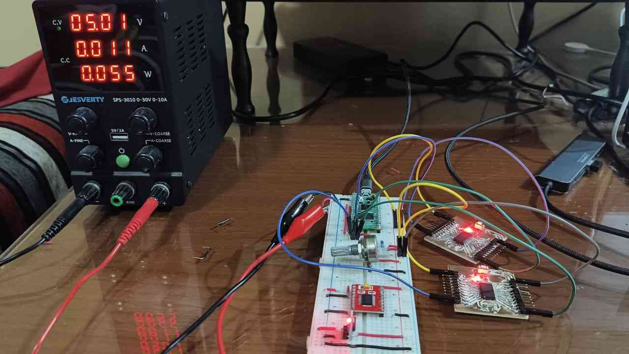
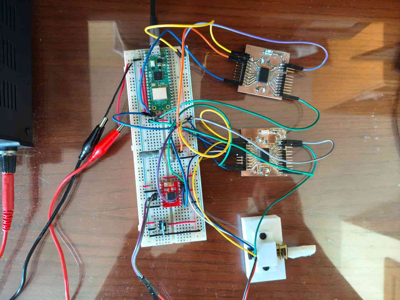
At that point in the Fab Academy, I assumed that the electronics for my robot would be a XIAO ESP32-C6 controlling four different Attiny 1616 microcontrollers. So I first attempted to use my XIAO ESP32-C6 for this assignment. However, I discovered that I had connected the I2C resistors between the corresponding GPIOs on the XIAO and the pin headers without using the pull-up configuration. Fortunately, my instructor told me to stick with the Raspberry Pi Pico 2 I had previously used. So I decided to redesign my system as a Raspberry Pi Pico 2 running two Attiny 1616 boards.
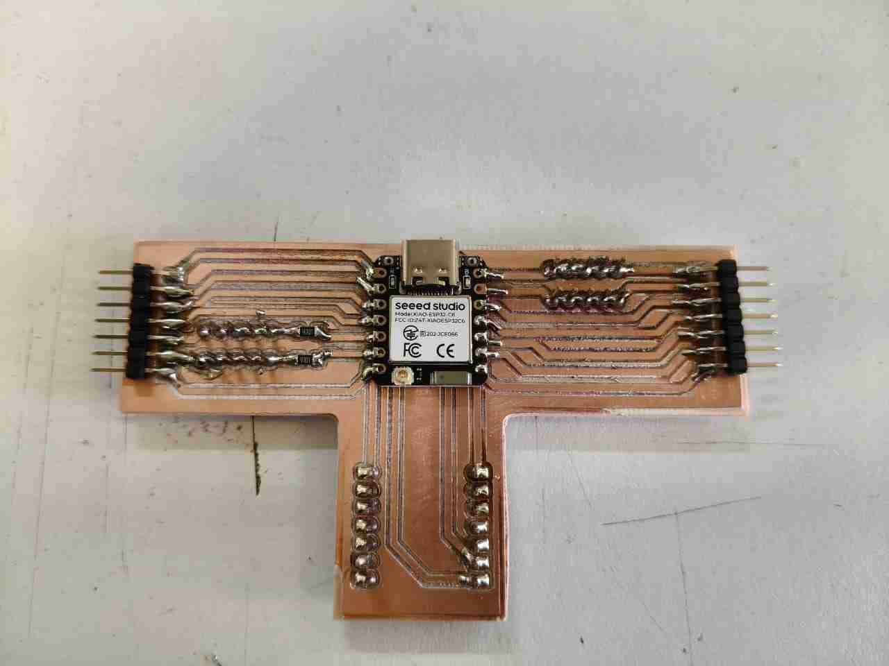
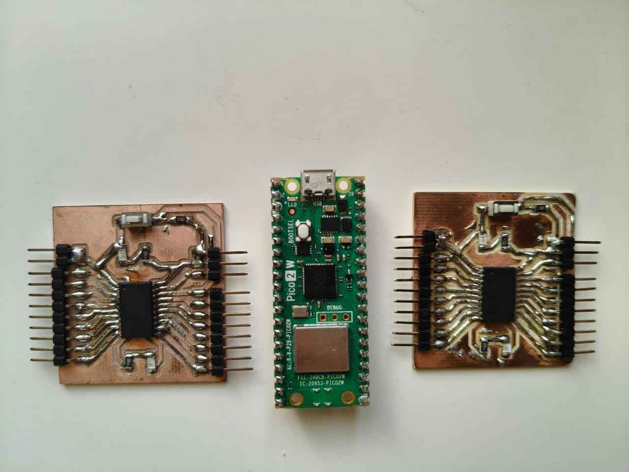
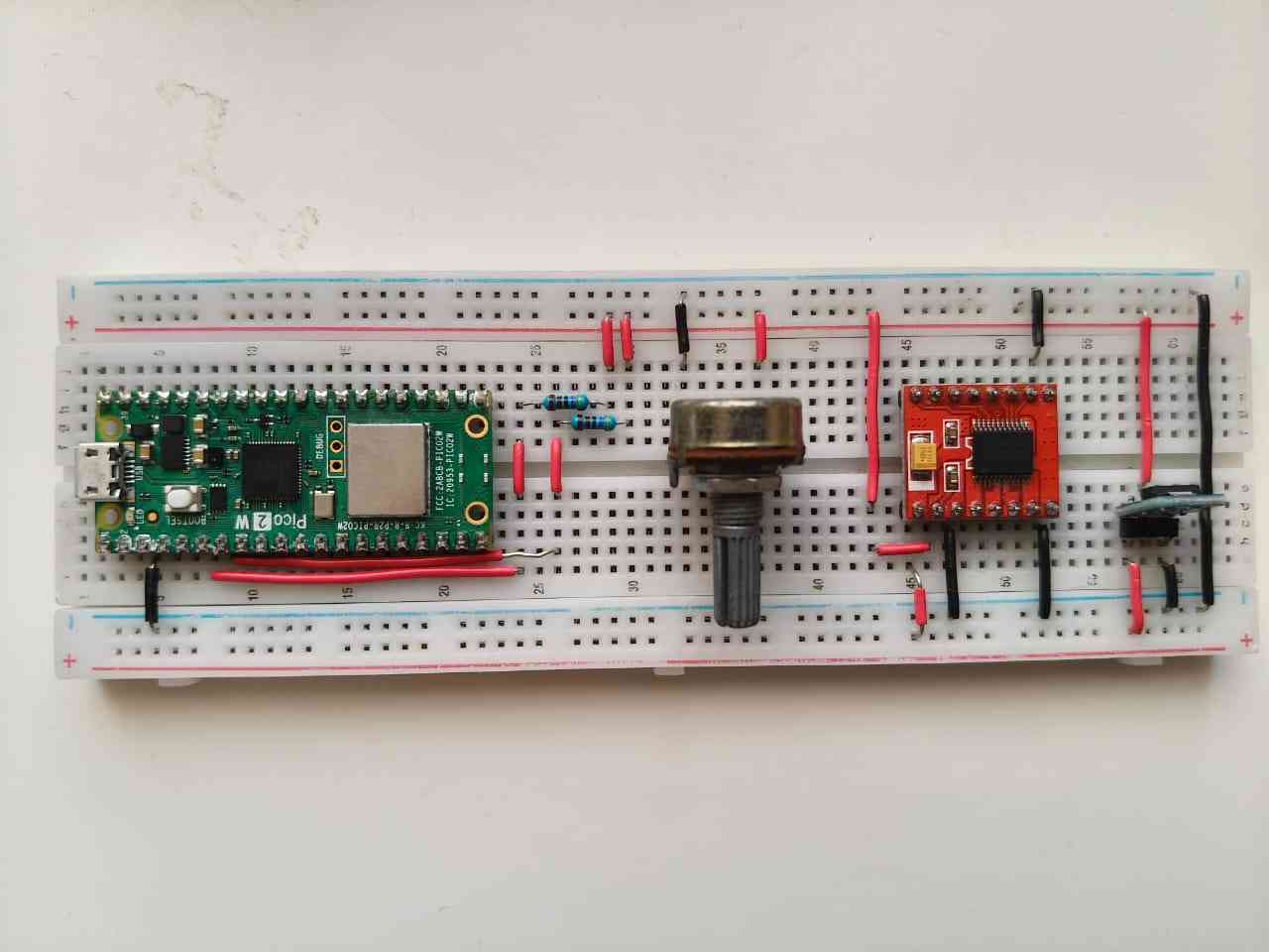
As my Raspberry Pi Pico 2 W board came with pin headers already soldered, I had to use a protoboard, which I'm not particularly fond of, but sometimes it can be effective. I inserted my Pico 2 into the protoboard, along with a potentiometer, a TB6612FNG driver, and the pull-up resistors for I2C. This time, I made sure to connect everything properly. The potentiometer and the driver will be utilized for a second activity within the assignment. First, I wanted to test the I2C connectivity between the Pico 2 and the Attiny boards.
Similar to the Week 10 assignment, I used an Arduino Nano to program my Attiny boards, following the same process outlined in that previous assignment.
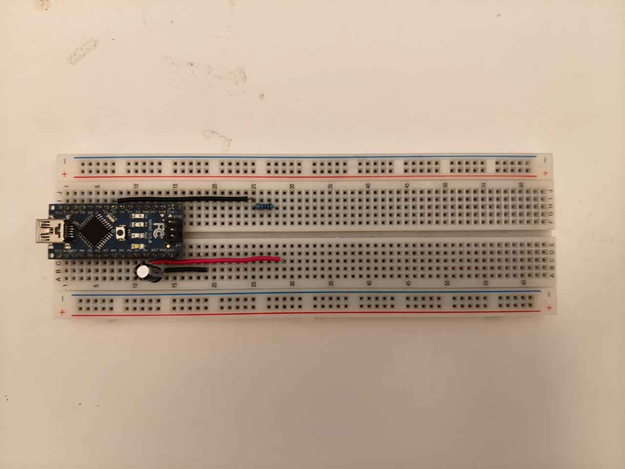
Arduino Nanoused as an ISP (In-System Programmer) to flash (program) an Attiny microcontroller.
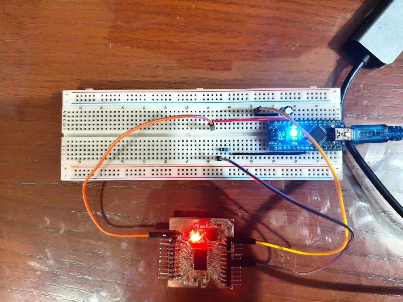
Throughout the assignment, both Attiny microcontrollers were powered by an external power supply, which also served as the power source for the TB6612FN-G driver.
Before beginning, I decided to assign an I2C address to each microcontroller. This would assist me later in determining whether I was retrieving information from the incorrect board or in identifying other potential issues.
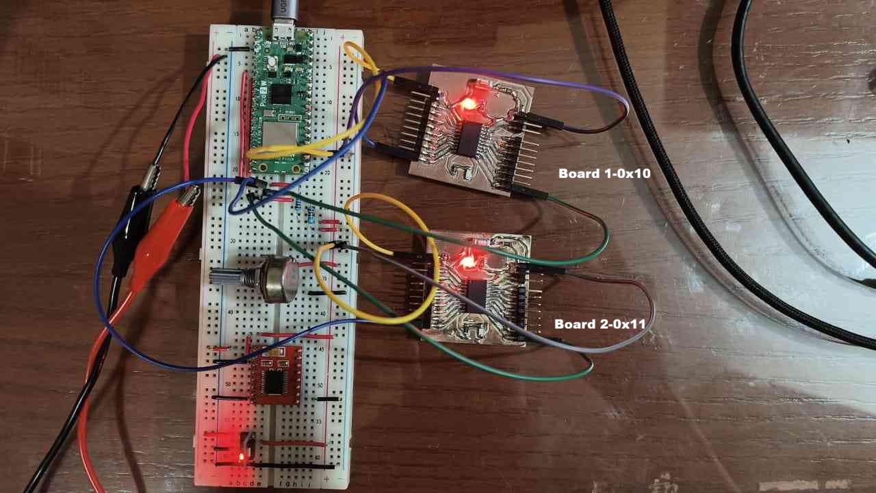
4. First Activity: Stablishing I2C Communication
For this initial activity, I aimed to test I2C communication between a device running Python and another device running Arduino. The objective was to use the Pico 2 as a controller to identify which ATtiny board had its button pressed, while also toggling the state of the corresponding LEDs. This would be achieved by sending commands from the controller to each ATtiny board.
Before I show the codes used, I want to emphasize that the easiest way to identify which devices are the controller or the target is to look for the line in the code that declares the address for its host device. Each target must have an I2C address, whereas controllers do not. Each target must have an I2C address, whereas controllers do not. As with other assignments, the following codes were written using assistance from Claude AI 's Sonnet 4.6 model.
Python code for the controller: Raspberry Pi Pico 2W
| Code | Role | What does it do? |
|---|---|---|
| from machine import I2C, Pin | Init | Imports MicroPython's hardware I2C driver. Uses the RP2350's I2C0 peripheral directly — not a software bit-bang implementation. |
| i2c = I2C(0, sda=Pin(4), scl=Pin(5), freq=100_000) | Init | Configures the I2C0 peripheral on GP4 (SDA) and GP5 (SCL) at 100 kHz (Standard mode). The Pico becomes the bus controller — it generates the clock and initiates all transactions. |
| i2c_lock = _thread.allocate_lock() | Lock | Creates a mutex shared between both cores. Prevents the polling thread and the command handler from accessing the I2C bus simultaneously, which would corrupt transactions. |
| with i2c_lock: i2c.writeto(addr, cmd) | Write | Acquires the lock, then sends a write transaction: START → target address + W bit → command byte → STOP. Only the addressed ATtiny responds; the other ignores it. |
| with i2c_lock: data = i2c.readfrom(addr, 1) | Poll | Acquires the lock, then sends a read transaction: START → target address + R bit → clock out 1 byte → NACK → STOP. The ATtiny's onRequest() fires and puts the status byte on SDA. |
| led_on = bool(status & 0x02) btn_pressed = bool(status & 0x01) | Decode | Unpacks the status byte using bitwise AND masks. 0x02 isolates Bit 1 (LED), 0x01 isolates Bit 0 (button). Mirrors exactly how the ATtiny packed them. |
| if btn_pressed and not prev['btn']: print("Button PRESSED") | Decode | Detects a rising edge on the button state — only prints when the state transitions from not-pressed to pressed, not on every poll. Avoids flooding the terminal. |
| _thread.start_new_thread( polling_thread, ()) | Poll | Launches polling_thread() on the second core (Core 1). It loops every 100ms reading both slaves. Core 0 stays free for blocking input() without freezing the poll. |
| devices = i2c.scan() | Scan | Iterates through all 127 possible I2C addresses, sending a probe write to each. Returns addresses that responded with ACK — used to verify 0x10 and 0x11 are visible on the bus. |
Here is the Python code for the controller (Raspberry Pi Pico 2W):
from machine import I2C, Pin
import utime
import _thread

# ── I2C setup ──
i2c = I2C(0, sda=Pin(4), scl=Pin(5), freq=100_000)
i2c_lock = _thread.allocate_lock()

# ── Target addresses ──
BOARDS = {
    '1': 0x10,
    '2': 0x11,
}

# ── Command bytes ──
CMD_LED_ON     = bytes([0x01])
CMD_LED_OFF    = bytes([0x02])
CMD_LED_TOGGLE = bytes([0x03])

# ── Last known states ──
last_state = {
    '1': {'led': None, 'btn': None},
    '2': {'led': None, 'btn': None},
}

# ─────────────────────────────────────────────
def scan_bus():
    with i2c_lock:
        devices = i2c.scan()
    if devices:
        print("Devices found on I2C bus:")
        for d in devices:
            label = ""
            for name, addr in BOARDS.items():
                if addr == d:
                    label = f"  ← Board {name}"
            print(f"  0x{d:02X}{label}")
    else:
        print("No devices found. Check wiring and pull-up resistors.")

def send_command(board_id, cmd_bytes):
    addr = BOARDS[board_id]
    try:
        with i2c_lock:
            i2c.writeto(addr, cmd_bytes)
        return True
    except OSError:
        print(f"  Error: Board {board_id} (0x{addr:02X}) not responding.")
        return False

def poll_board(board_id):
    addr = BOARDS[board_id]
    try:
        with i2c_lock:
            data = i2c.readfrom(addr, 1)
        status = data[0]

        led_on      = bool(status & 0x02)
        btn_pressed = bool(status & 0x01)
        prev        = last_state[board_id]

        if prev['led'] is not None and led_on != prev['led']:
            print(f"\n  [Board {board_id}] LED → {'ON' if led_on else 'OFF'}")

        if prev['btn'] is not None and btn_pressed and not prev['btn']:
            print(f"\n  [Board {board_id}] Button PRESSED")

        if prev['btn'] is not None and not btn_pressed and prev['btn']:
            print(f"\n  [Board {board_id}] Button released")

        last_state[board_id]['led'] = led_on
        last_state[board_id]['btn'] = btn_pressed

    except OSError:
        pass

def polling_thread():
    """Runs on second core — polls both targets every 100ms."""
    while True:
        for board_id in BOARDS:
            poll_board(board_id)
        utime.sleep_ms(100)

def show_help():
    print("─" * 40)
    print("  Commands:")
    print("  1 on      LED ON  — board 1")
    print("  1 off     LED OFF — board 1")
    print("  1 toggle  Toggle  — board 1")
    print("  2 on      LED ON  — board 2")
    print("  2 off     LED OFF — board 2")
    print("  2 toggle  Toggle  — board 2")
    print("  scan      Scan I2C bus")
    print("  help      Show this list")
    print("─" * 40)

def process(line):
    parts = line.strip().lower().split()
    if not parts:
        return

    if parts[0] == 'scan':
        scan_bus()
        return

    if parts[0] == 'help':
        show_help()
        return

    if len(parts) < 2:
        print("  Unknown command. Type 'help' for options.")
        return

    board_id, action = parts[0], parts[1]

    if board_id not in BOARDS:
        print(f"  Unknown board '{board_id}'. Use 1 or 2.")
        return

    if action == 'on':
        send_command(board_id, CMD_LED_ON)
    elif action == 'off':
        send_command(board_id, CMD_LED_OFF)
    elif action == 'toggle':
        send_command(board_id, CMD_LED_TOGGLE)
    else:
        print(f"  Unknown action '{action}'. Type 'help' for options.")

# ─────────────────────────────────────────────
print("Pico 2W I2C Controller — ready")
print("Type 'help' for commands, 'scan' to detect targets.")
print()

# Start polling on second core (Pico 2W has dual cores)
_thread.start_new_thread(polling_thread, ())

# Main core handles serial input normally
while True:
    try:
        line = input(">> ")
        process(line)
    except KeyboardInterrupt:
        print("\nStopped.")
        break
Arduino Code for targets (Attiny 1616 boards)
| Code | Role | What does it do? |
|---|---|---|
| #include <Wire.h> | Init | Loads the Wire library, which wraps the ATtiny1616's hardware TWI peripheral. Without this, no I2C functions are available. |
| Wire.begin(I2C_ADDRESS) | Init | Starts the TWI peripheral in target mode at the given 7-bit address (0x10 or 0x11). The ATtiny will only respond when the controller addresses it specifically. |
| Wire.onReceive(onReceive) | Receive | Registers a callback interrupt. When the Pico writes bytes to this target's address, the TWI hardware fires an interrupt and calls onReceive() automatically. |
| Wire.onRequest(onRequest) | Send | Registers a callback interrupt. When the Pico issues a read request to this address, the TWI hardware calls onRequest() so the ATtiny can load a reply byte. |
| uint8_t cmd = Wire.read() | Receive | Inside onReceive() — reads one byte from the TWI receive buffer. This byte is the command sent by the controller (0x01 ON, 0x02 OFF, 0x03 TOGGLE). |
| uint8_t status = 0x00; if (ledState) status |= 0x02; if (btnPressed) status |= 0x01; | Send | Inside onRequest() — loads the packed status byte into the TWI transmit buffer. The hardware sends it over SDA as soon as the Pico clocks it out. |
| Wire.write(status) | Send | Inside onRequest() — loads the packed status byte into the TWI transmit buffer. The hardware sends it over SDA as soon as the Pico clocks it out. |
| bool btnPressed = (digitalRead(PIN_BUTTON) == HIGH) | Pack | Reads the button pin just before replying. HIGH = pressed because INPUT_PULLUP inverts the logic — pin is LOW at rest, HIGH when button shorts it to 3.3V. |
Here is the Python code for the targets (Attiny 1616 boards):
          #include <Wire.h>

          // ── Change this ONE line when flashing the second board ──
          #define I2C_ADDRESS  0x10   // Board 1 → 0x10 | Board 2 → 0x11
          // ─────────────────────────────────────────────────────────

          #define PIN_LED     PIN_PA1
          #define PIN_BUTTON  PIN_PA2

          volatile bool ledState = false;

          // ── Called when Pico WRITES to this target ──
          void onReceive(int numBytes) {
            while (Wire.available()) {
              uint8_t cmd = Wire.read();
              switch (cmd) {
                case 0x01:                      // LED ON
                  ledState = true;
                  digitalWrite(PIN_LED, HIGH);
                  break;
                case 0x02:                      // LED OFF
                  ledState = false;
                  digitalWrite(PIN_LED, LOW);
                  break;
                case 0x03:                      // LED TOGGLE
                  ledState = !ledState;
                  digitalWrite(PIN_LED, ledState ? HIGH : LOW);
                  break;
                default:
                  break;
              }
            }
          }

          // ── Called when Pico READS from this target ──
          void onRequest() {
            bool btnPressed = (digitalRead(PIN_BUTTON) == HIGH);
            // Pack both states into 1 byte
            // Bit 1 = LED, Bit 0 = Button
            uint8_t status = 0x00;
            if (ledState)   status |= 0x02;
            if (btnPressed) status |= 0x01;
            Wire.write(status);
          }

          void setup() {
            pinMode(PIN_LED,    OUTPUT);
            pinMode(PIN_BUTTON, INPUT_PULLUP);
            digitalWrite(PIN_LED, LOW);

            Wire.begin(I2C_ADDRESS);
            Wire.onReceive(onReceive);
            Wire.onRequest(onRequest);
          }

          void loop() {
            // Nothing here — all handled by Wire callbacks
          }
Controller code running on thonny
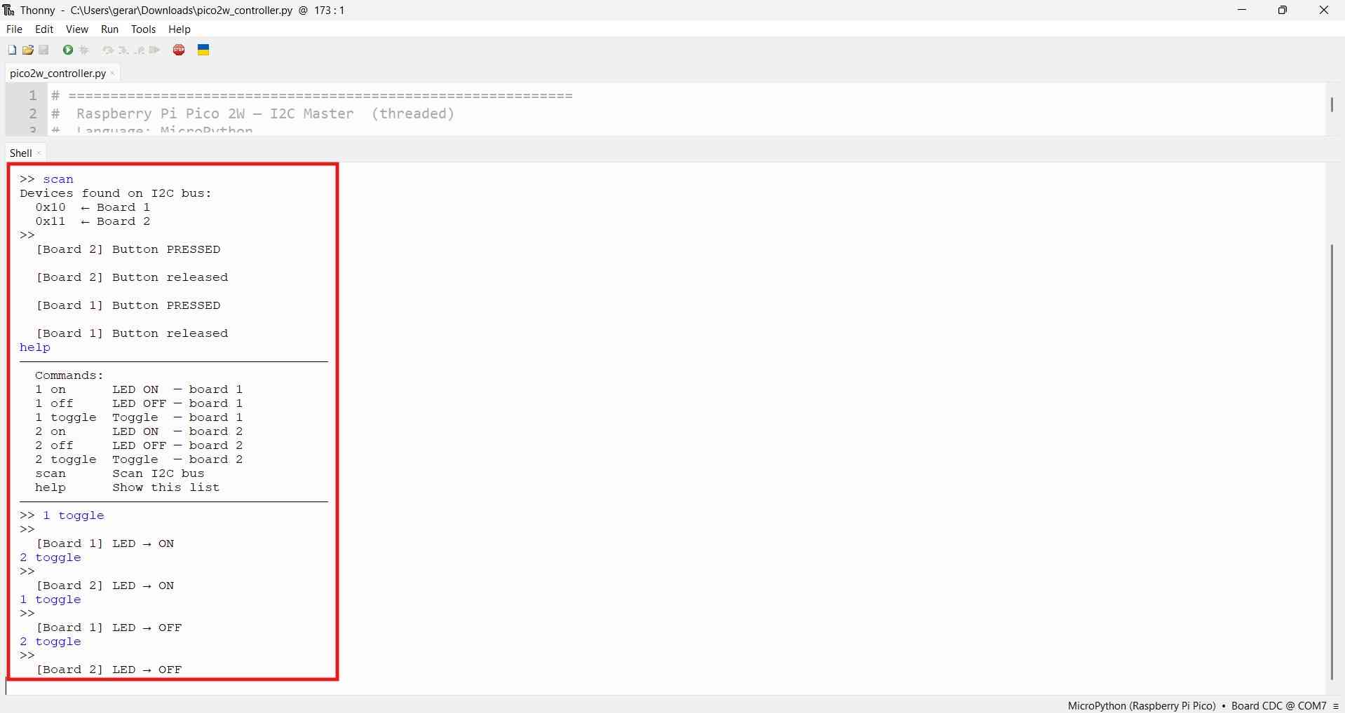
Video evidences of the system working as intended:
5. Second Activity: Using one Attiny 1616 as a controller for a motor connected to a second Attiny 1616 managed by a Raspberry Pi Pico 2W
After validating the I2C communication protocol implemented in my system, I wanted to explore a project that was more aligned with my final objectives. I planned to connect a potentiometer to the first ATtiny, allowing it to function as a motor speed controller, with the onboard motor serving as the start/stop control. The second ATtiny would be paired with a TB6612FNG driver and a micro metal gear motor equipped with a quadrature encoder. This ATtiny would read the encoder pulse counts and respond to the commands sent from the controller ATtiny. The Pico 2W would act as the intermediary between both ATtinys and help the user visualize the motor's state and speed.
Python code for the controller: Raspberry Pi Pico 2W
| Code | Role | What does it do? |
|---|---|---|
| i2c = I2C(0, sda=Pin(4), scl=Pin(5), freq=100_000) i2c_lock = _thread.allocate_lock() | Init | Configures I2C0 as controller and creates a mutex so Core 0 (serial) and Core 1 (polling) never access the bus simultaneously. |
| with i2c_lock: data = i2c.readfrom(ADDR_POT, 2) speed = data[0] running = bool(data[1]) | Poll | Reads 2 bytes from Board 1 every 100ms: Byte 0 = pot speed, Byte 1 = motor toggle state. Compared against previous values to detect changes. |
| with i2c_lock: i2c.writeto(ADDR_MOTOR, bytes([speed, 1 if running else 0])) | Forward | Forwards speed and run state to Board 2 only when something changed since the last poll — avoids flooding the bus with redundant writes. |
| with i2c_lock: data = i2c.readfrom(ADDR_MOTOR, 2) rpm = (data[0] << 8) | data[1] | Poll | Reads 2 bytes from Board 2 and reassembles the uint16 RPM value with a left shift on the high byte and bitwise OR with the low byte. |
| _thread.start_new_thread( coordinator_thread, ()) | Thread | Runs the full read→forward→read loop on Core 1. Core 0 stays free for blocking input() in the Thonny shell without freezing the poll. |
        from machine import I2C, Pin
        import utime
        import _thread

        # ── I2C setup ──
        i2c      = I2C(0, sda=Pin(4), scl=Pin(5), freq=100_000)
        i2c_lock = _thread.allocate_lock()

        # ── Addresses ──
        ADDR_POT   = 0x10
        ADDR_MOTOR = 0x11

        # ── Shared state ──
        state = {
            'speed':        0,
            'running':      False,
            'rpm':          0,
            'prev_speed':   -1,
            'prev_running': None,
            'prev_rpm':     -1,
        }
        state_lock = _thread.allocate_lock()

        # ─────────────────────────────────────────────
        def scan_bus():
            with i2c_lock:
                devices = i2c.scan()
            names = {ADDR_POT: 'Board 1 (pot+button)', ADDR_MOTOR: 'Board 2 (motor)'}
            if devices:
                print("Devices found:")
                for d in devices:
                    print(f"  0x{d:02X} — {names.get(d, 'unknown')}")
            else:
                print("No devices found. Check wiring.")

        def read_board1():
            try:
                with i2c_lock:
                    data = i2c.readfrom(ADDR_POT, 2)
                return data[0], bool(data[1])
            except OSError:
                return None, None

        def send_board2(speed, running):
            try:
                with i2c_lock:
                    i2c.writeto(ADDR_MOTOR, bytes([speed, 1 if running else 0]))
            except OSError:
                pass

        def read_rpm():
            try:
                with i2c_lock:
                    data = i2c.readfrom(ADDR_MOTOR, 2)
                return (data[0] << 8) | data[1]
            except OSError:
                return None

        def print_status_line(speed, running, rpm):
            motor_str = "RUNNING" if running else "STOPPED"
            rpm_str   = str(rpm) if running else "—"
            print(f"  → Speed: {speed:3d}%  |  Motor: {motor_str}  |  RPM: {rpm_str}")

        def show_help():
            print("─" * 44)
            print("  scan    — detect I2C devices")
            print("  status  — print current state")
            print("  help    — show this list")
            print("─" * 44)

        def process(line):
            cmd = line.strip().lower()
            if cmd == 'scan':
                scan_bus()
            elif cmd == 'status':
                with state_lock:
                    print_status_line(state['speed'], state['running'], state['rpm'])
            elif cmd == 'help':
                show_help()
            elif cmd:
                print("  Unknown command. Type 'help'.")

        # ─────────────────────────────────────────────
        def coordinator_thread():
            while True:
                speed, running = read_board1()

                if speed is not None:
                    # Forward to Board 2 if changed
                    with state_lock:
                        prev_speed   = state['prev_speed']
                        prev_running = state['prev_running']

                    if speed != prev_speed or running != prev_running:
                        send_board2(speed, running)
                        with state_lock:
                            state['speed']        = speed
                            state['running']      = running
                            state['prev_speed']   = speed
                            state['prev_running'] = running

                # Always read RPM from Board 2
                rpm = read_rpm()
                if rpm is None:
                    rpm = 0

                with state_lock:
                    state['rpm'] = rpm

                # ── Print one unified line if anything changed ──
                with state_lock:
                    s   = state['speed']
                    r   = state['running']
                    rpm = state['rpm']
                    ps  = state['prev_speed']
                    pr  = state['prev_running']
                    prpm = state['prev_rpm']

                rpm_changed   = abs(rpm - prpm) > 2
                state_changed = (s != ps) or (r != pr)

                if state_changed or rpm_changed:
                    print_status_line(s, r, rpm)
                    with state_lock:
                        state['prev_speed']   = s
                        state['prev_running'] = r
                        state['prev_rpm']     = rpm

                utime.sleep_ms(100)

        # ─────────────────────────────────────────────
        print("Pico 2W — Motor Coordinator — ready")
        print("Type 'help' for commands, 'scan' to detect boards.")
        print()

        _thread.start_new_thread(coordinator_thread, ())

        while True:
            try:
                line = input(">> ")
                process(line)
            except KeyboardInterrupt:
                print("\nStopped.")
                break
Arduino Code for controller Attiny
| Code | Role | What does it do? |
|---|---|---|
| Wire.begin(I2C_ADDRESS) Wire.onReceive(onReceive) Wire.onRequest(onRequest) | Init | Starts TWI in target mode at 0x11. Registers both callbacks — this target both receives motor commands and sends RPM back. |
| uint16_t raw = analogRead(PIN_POT) uint8_t speed = map(raw,0,1023,0,100) | Pack | Reads the ADC on PA4 (0–1023) and maps it to 0–100. Called inside onRequest() so the value is always fresh at the moment the controller reads it. |
| Wire.write(speed) Wire.write(state) | Send | Loads 2 bytes into the TWI transmit buffer: Byte 0 = speed (0–100), Byte 1 = motor toggle state (1 = run, 0 = stop). |
| if (btnReading == LOW && btnStatePrev == HIGH) { motorRunning = !motorRunning; } | Pack | Detects a falling edge after debounce stabilises. Toggles motorRunning which is included in the next I2C reply byte. |
            #include
            #define I2C_ADDRESS  0x10

            #define PIN_LED     PIN_PA1
            #define PIN_BUTTON  PIN_PA2
            #define PIN_POT     PIN_PA4

            // ── State ──
            volatile bool motorRunning = false;

            bool     btnStatePrev  = HIGH;  // previous stable button state
            bool     btnReading    = HIGH;  // current raw reading
            uint32_t debounceStart = 0;
            const uint16_t DEBOUNCE_MS = 40;

            // ── Called when Pico READS from this target ──
            void onRequest() {
              uint16_t raw   = analogRead(PIN_POT);
              uint8_t  speed = (uint8_t)map(raw, 0, 1023, 0, 100);
              uint8_t  state = motorRunning ? 1 : 0;
              Wire.write(speed);
              Wire.write(state);
            }

            void onReceive(int numBytes) {
              while (Wire.available()) Wire.read();
            }

            void setup() {
              pinMode(PIN_LED,    OUTPUT);
              pinMode(PIN_BUTTON, INPUT_PULLUP);
              analogReference(VDD);
              digitalWrite(PIN_LED, LOW);

              Wire.begin(I2C_ADDRESS);
              Wire.onRequest(onRequest);
              Wire.onReceive(onReceive);
            }

            void loop() {
              bool currentReading = digitalRead(PIN_BUTTON);

              // If reading changed, reset debounce timer
              if (currentReading != btnReading) {
                btnReading    = currentReading;
                debounceStart = millis();
              }

              // Only act if reading has been stable for DEBOUNCE_MS
              if ((millis() - debounceStart) >= DEBOUNCE_MS) {
                // Detect falling edge on stable state: HIGH → LOW = press
                if (btnReading == LOW && btnStatePrev == HIGH) {
                  motorRunning = !motorRunning;
                  digitalWrite(PIN_LED, motorRunning ? HIGH : LOW);
                }
                btnStatePrev = btnReading;
              }
            }
Arduino code for Motor attiny
| Code | Role | What does it do? |
|---|---|---|
| Wire.begin(I2C_ADDRESS) Wire.onRequest(onRequest) Wire.onReceive(onReceive) | Init | Starts TWI in target mode at 0x10 and registers both callbacks. This target is read-only — onReceive just flushes any unexpected writes. |
| uint8_t spd = Wire.read() uint8_t state = Wire.read() targetSpeed = constrain(spd, 0, 100) motorRun = (state == 1) | Receive | Reads 2 command bytes from TWI buffer inside onReceive(): Byte 0 = speed 0–100, Byte 1 = run/stop. Values stored as volatile for use in loop(). |
| Wire.write((currentRPM >> 8) & 0xFF) Wire.write(currentRPM & 0xFF) | Send | Sends RPM as a uint16 big-endian (2 bytes) inside onRequest(). High byte first, low byte second — controller reassembles with a left shift. |
| attachInterrupt( digitalPinToInterrupt(PIN_ENC_A), encoderISR, RISING) | Encode | Counts rising edges on encoder channel A via hardware interrupt. Used to calculate RPM: delta counts × 60000 / (PPR × elapsed ms). |
| currentRPM = (delta * 60000UL) / (COUNTS_PER_REV * elapsed) | Encode | Recalculates RPM every 200ms using encoder pulse delta. Result stored in currentRPM ready for the next onRequest() call. |
            #include
            #define I2C_ADDRESS  0x11

            #define PIN_LED      PIN_PA1
            #define PIN_IN1      PIN_PA4
            #define PIN_IN2      PIN_PA5
            #define PIN_PWM      PIN_PB2
            #define PIN_ENC_A    PIN_PA6
            #define PIN_ENC_B    PIN_PA7

            // ── Encoder constants ──
            // 7 PPR × 298 gearbox ratio × 2 edges (rising only on A) = 4172
            const uint32_t COUNTS_PER_REV = 4172UL;

            // ── Volatile encoder state ──
            volatile uint32_t encoderCount = 0;

            // ── Motor state (updated by I2C) ──
            volatile uint8_t  targetSpeed = 0;    // 0–100
            volatile bool     motorRun    = false;

            // ── RPM calculation ──
            uint16_t currentRPM   = 0;
            uint32_t lastRPMTime  = 0;
            uint32_t lastCount    = 0;
            const uint16_t RPM_INTERVAL_MS = 200; // recalculate every 200ms

            // ── Encoder ISR — rising edge on channel A ──
            void encoderISR() {
              encoderCount++;
            }

            // ── Called when Pico WRITES to this target ──
            void onReceive(int numBytes) {
              if (numBytes >= 2) {
                uint8_t spd   = Wire.read();
                uint8_t state = Wire.read();
                targetSpeed = constrain(spd, 0, 100);
                motorRun    = (state == 1);
              }
              while (Wire.available()) Wire.read(); // flush extras
            }

            // ── Called when Pico READS from this target ──
            void onRequest() {
              // Send RPM as uint16 big-endian
              Wire.write((currentRPM >> 8) & 0xFF);  // high byte
              Wire.write(currentRPM & 0xFF);          // low byte
            }

            void setMotor(uint8_t speed0to100, bool run) {
              if (!run || speed0to100 == 0) {
                // Stop — brake mode
                digitalWrite(PIN_IN1, HIGH);
                digitalWrite(PIN_IN2, HIGH);
                analogWrite(PIN_PWM, 0);
                digitalWrite(PIN_LED, LOW);
              } else {
                // Forward
                digitalWrite(PIN_IN1, HIGH);
                digitalWrite(PIN_IN2, LOW);
                uint8_t pwmVal = map(speed0to100, 0, 100, 0, 255);
                analogWrite(PIN_PWM, pwmVal);
                digitalWrite(PIN_LED, HIGH);
              }
            }

            void setup() {
              pinMode(PIN_LED,   OUTPUT);
              pinMode(PIN_IN1,   OUTPUT);
              pinMode(PIN_IN2,   OUTPUT);
              pinMode(PIN_PWM,   OUTPUT);
              pinMode(PIN_ENC_A, INPUT);
              pinMode(PIN_ENC_B, INPUT);

              digitalWrite(PIN_LED, LOW);
              setMotor(0, false);

              // Interrupt on rising edge of encoder A
              attachInterrupt(digitalPinToInterrupt(PIN_ENC_A), encoderISR, RISING);

              Wire.begin(I2C_ADDRESS);
              Wire.onReceive(onReceive);
              Wire.onRequest(onRequest);

              lastRPMTime = millis();
            }

            void loop() {
              // ── Update motor output ──
              setMotor(targetSpeed, motorRun);

              // ── Recalculate RPM every RPM_INTERVAL_MS ──
              uint32_t now = millis();
              if (now - lastRPMTime >= RPM_INTERVAL_MS) {
                // Snapshot encoder count safely
                noInterrupts();
                uint32_t count = encoderCount;
                interrupts();

                uint32_t delta    = count - lastCount;
                uint32_t elapsed  = now - lastRPMTime;

                // RPM = (delta / COUNTS_PER_REV) / (elapsed / 60000)
                //     = delta * 60000 / (COUNTS_PER_REV * elapsed)
                currentRPM = (uint16_t)((delta * 60000UL) / (COUNTS_PER_REV * elapsed));

                lastCount   = count;
                lastRPMTime = now;
              }
            }
Video evidence of the system working as intended:
6. Files
Here are the downloadable files for this week:
Python and arduino codes for the motor activityReflection
I have used I2C before, and in my original robot, all my microcontrollers communicated with each other using it. However, this assignment provided me with valuable experience using I2C with the Attiny microcontrollers, which I am still getting accustomed to. I hope that what I learned here will be useful in the future.