Week 8: Electronics design
Before starting
A Printed Circuit Board (PCB) is a platform used to mechanically support and electrically connect electronic components through conductive copper traces etched onto a non-conductive substrate. PCBs are a fundamental element in modern electronics, as they allow circuits to be compact, robust, and reproducible.Compared to a protoboard, PCBs offer several important advantages. While protoboard are ideal for rapid prototyping and testing due to their flexibility and reusability, they suffer from loose connections, susceptibility to noise, and limited current handling.
In contrast, PCBs provide stable electrical connections, reduced interference, improved signal integrity, and a much more compact and professional layout. This makes them suitable for final products and long-term use.
There are several types of PCBs depending on their complexity:
Single layer:
Which have one conductive layer and are used for simple circuits.
Double layer:
Which allow routing on both sides, improving space usage and design flexibility.
Multi layer:
Which consist of multiple stacked layers and are used in complex systems such as computers and embedded devices.
- Importing the PCB design (usually in Gerber format).
- Milling the copper layer to isolate the traces (removing unwanted copper).
- Cutting the board outline (edge cuts).
- Soldering the components onto the board.
Regarding components, modern PCB design heavily relies on Surface Mount Devices (SMD). These components are mounted directly onto the surface of the PCB, unlike traditional through-hole components, which require holes drilled through the board. SMD components offer several advantages:
- Smaller size, enabling compact designs.
- Better performance at high frequencies.
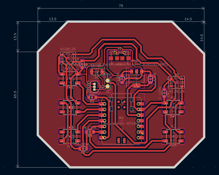
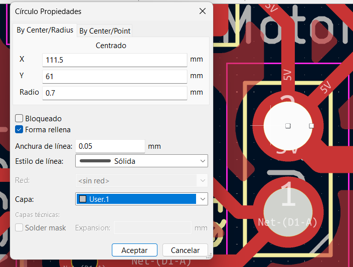
Additionally, designing a PCB involves considering factors such as power distribution, grounding (GND planes), trace width, and component placement, all of which impact the performance and reliability of the circuit. For example, adding a copper pour (like in the week6) to reduce noise, improves current return paths, and simplifies routing.
For further information about this topic and the machines at IBERO Puebla, please consult this week’s group page.
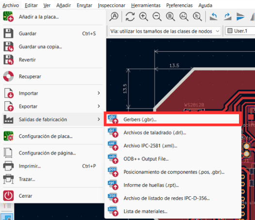
Export files
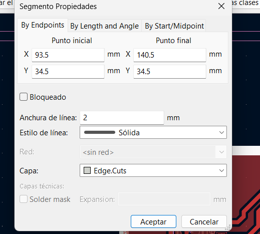
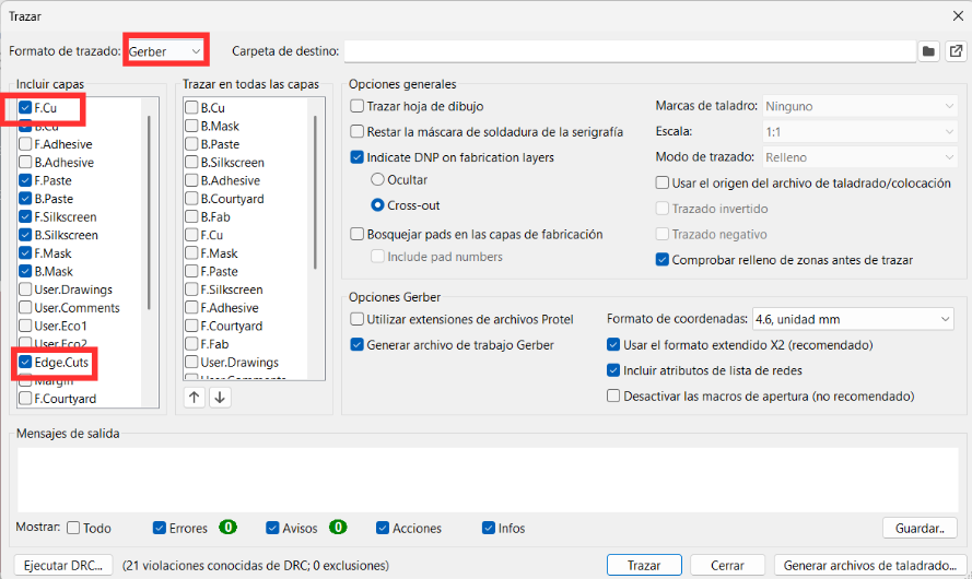
The board outline must be placed on the Edge.Cuts layer, as this defines the physical shape of the PCB. Since the milling tool that will be used has a diameter of 2 mm, the outline must be designed with a line width equal to or greater than this value to ensure proper cutting and avoid inaccuracies during fabrication.
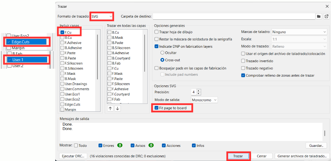
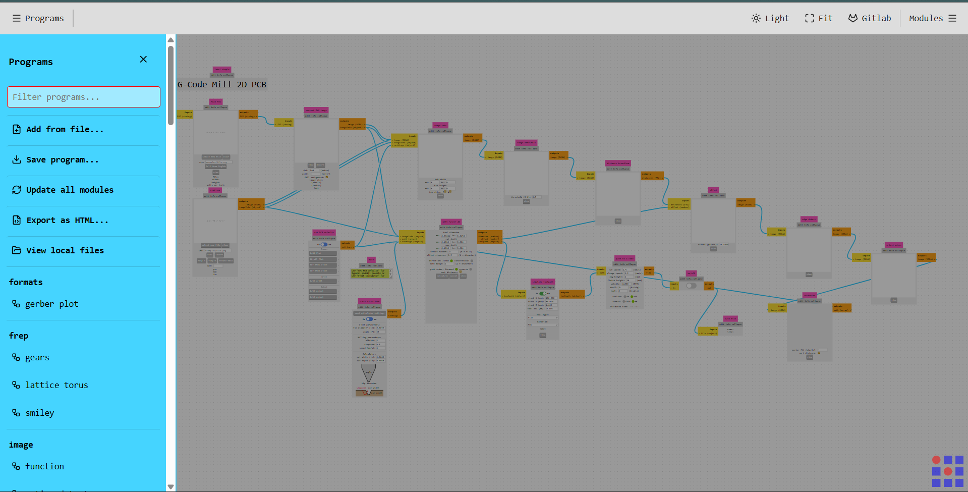
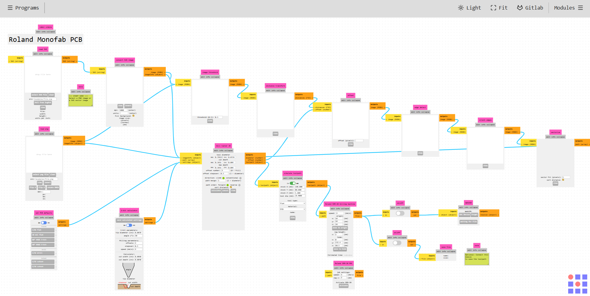
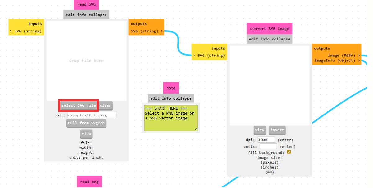
- Change the output format to SVG, since this format is compatible with the MonoFab workflow.
- Select each of the previously defined layers individually (such as traces, Edge.Cuts, and User layers).
- Enable the option “Fit page to board” to ensure the design scales correctly.
- Finally, click on “Plot” to generate the files.
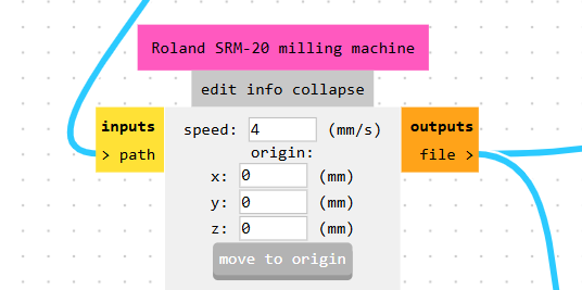
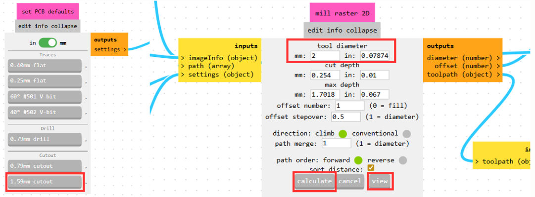
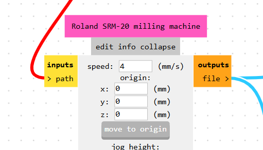
Within this platform, a wide variety of machines can be selected from the left-hand menu. In this case, the Roland SRM-20 milling machine was chosen under the “mill 2D PCB” option.
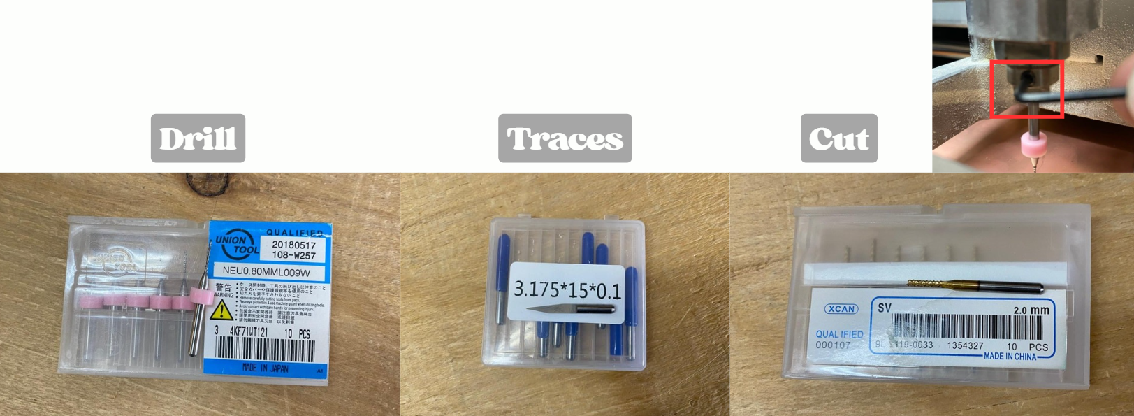
Drilling Process
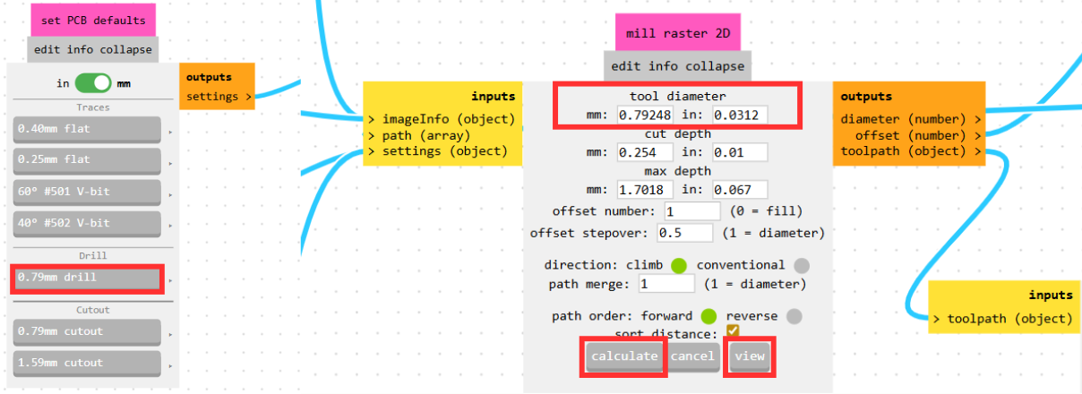
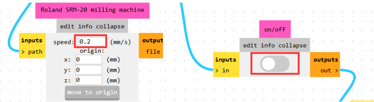
For drilling operations, a 0.79 mm drill bit is used. Before exporting the toolpath, it is necessary to adjust the feed rate in the Roland SRM-20 milling machine module to 0.2 mm/s, which helps prevent tool breakage due to excessive stress.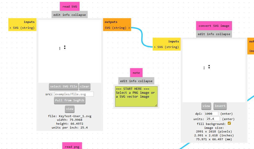
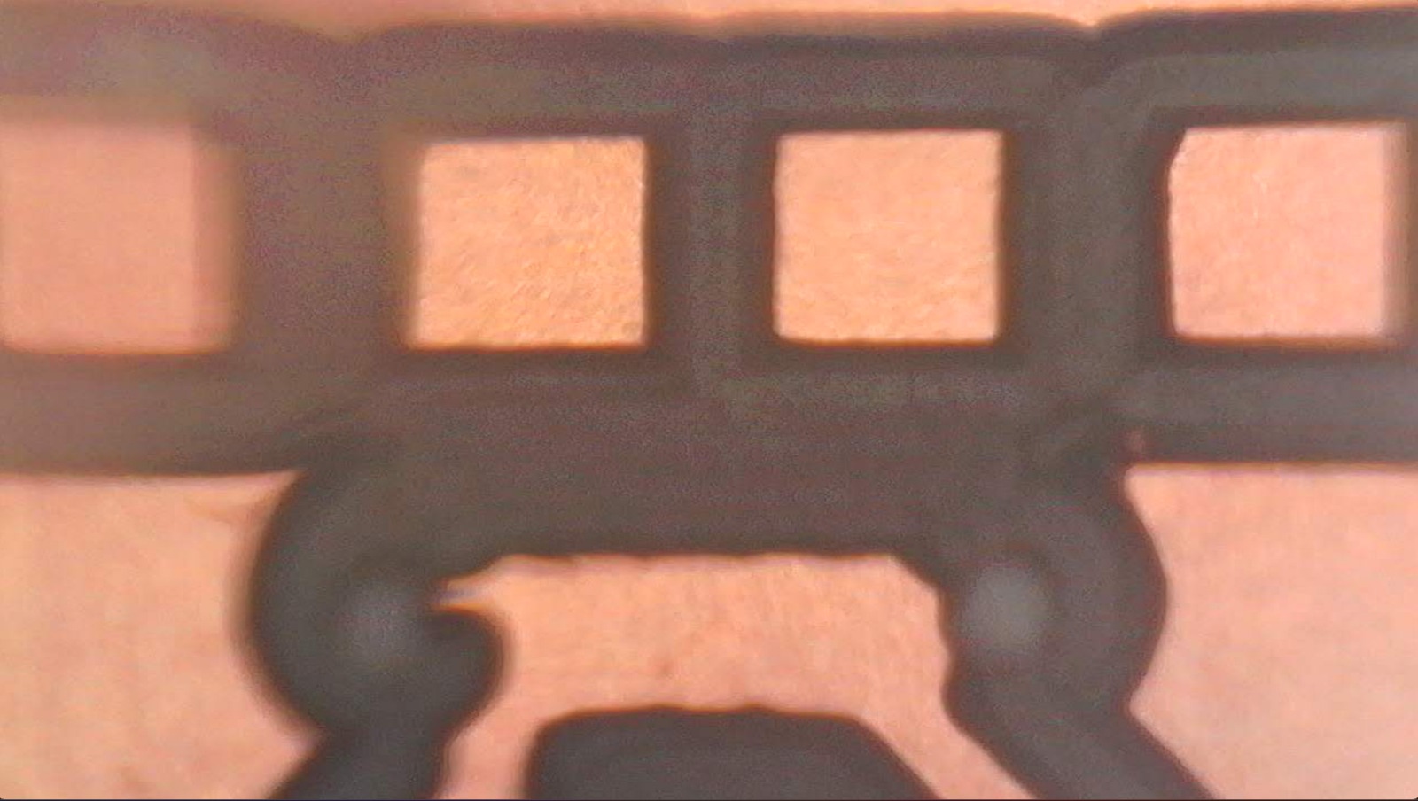
An important detail is that some holes, such as those for the transistor, may not appear. This occurs because the drill bit diameter is larger than the hole size defined in the design, making it impossible for the tool to reproduce those features accurately.
Traces Milling
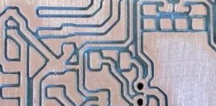
The process for milling traces is similar, but with a key difference. When importing the SVG, the traces may appear in black, which indicates that they will be removed this is incorrect for PCB traces.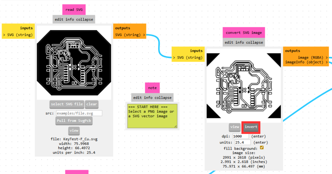
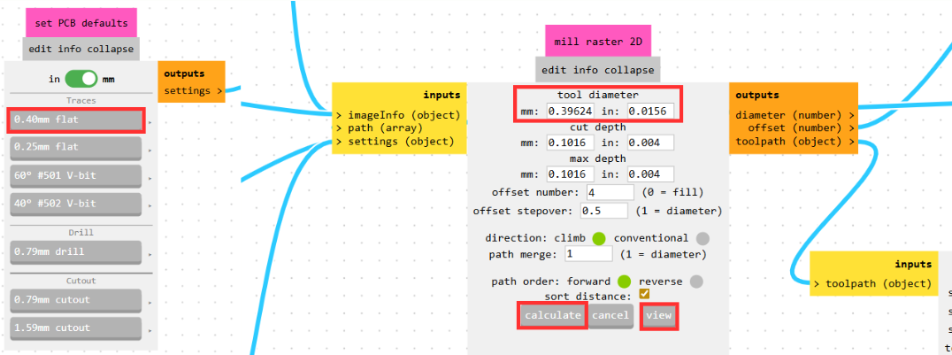
A limitationobserved in this stage is that small features, such as micro-USB pins, may appear merged in the preview. This happens because the tool diameter is too large to properly isolate such fine details, which is an important consideration when designing for CNC milling.
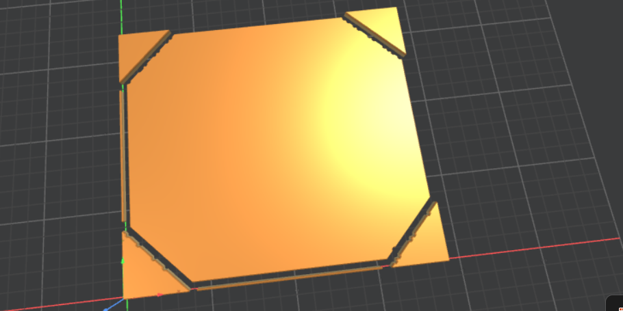
Board Outline
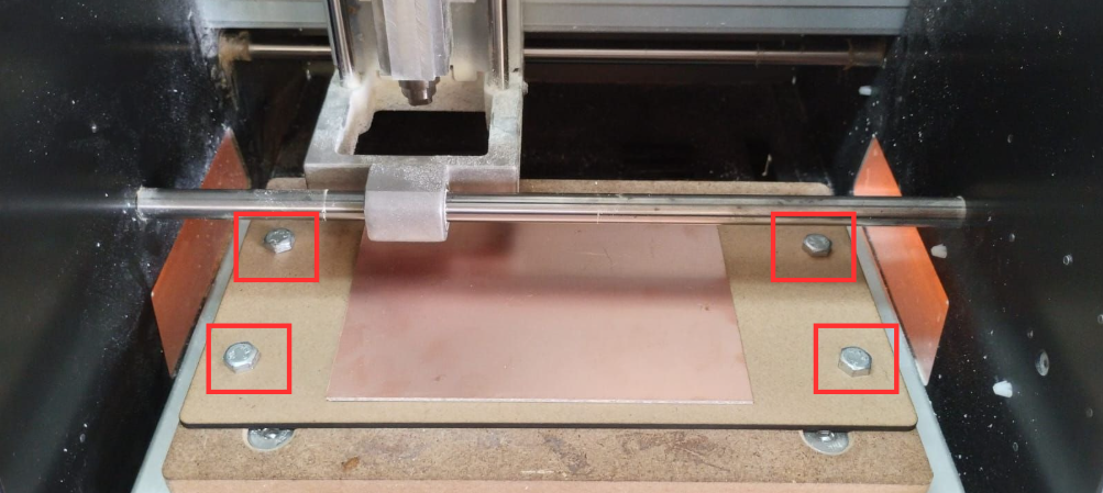
Finally, for cutting the board outline, a 1.59 mm cutout tool is used with a feed rate of 4 mm/s, maintaining the origin at (0,0,0).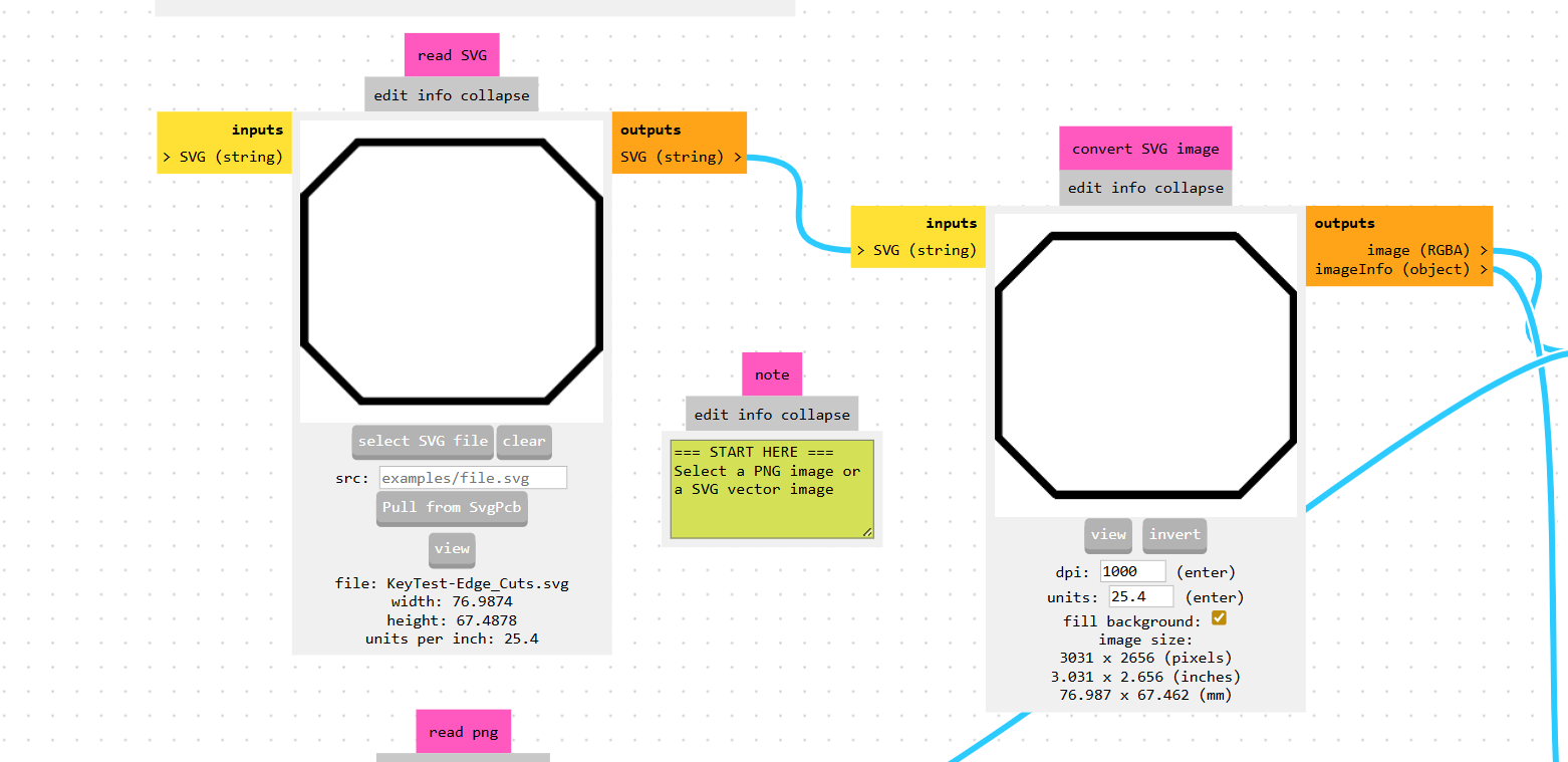
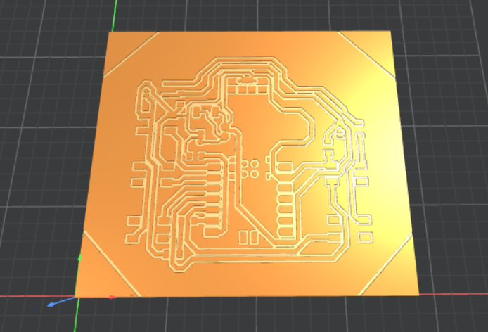
Board
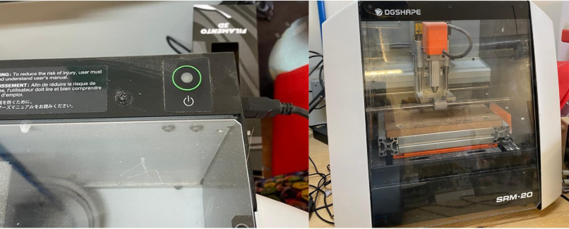
SRM-20 by DGSHAPE
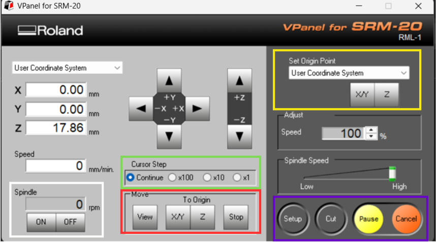
Set Origin Point:
This is used to define the reference position of the machine. The X/Y axes are set to establish the horizontal origin, and the Z axis is set separately to define the vertical starting point.
Move:
This option allows manual positioning of the toolhead to locate the origin or move to a specific point on the board.
Cursor Step:
Adjusts the step size or speed of manual movements, enabling fine or coarse positioning depending on the need.
Spindle:
Controls the rotation of the milling spindle. It is especially useful when setting the Z axis, as the tool can be carefully lowered without applying excessive force that could damage it.
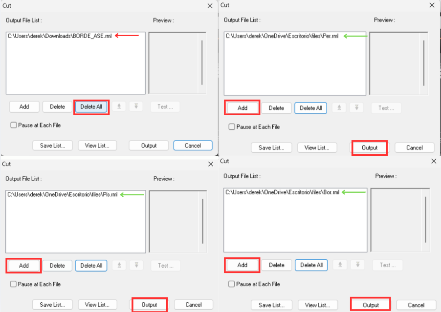
Process Controls
These manage the execution of the machining jobs.
- Click “Delete All” to remove any previously loaded jobs.
- Click “Add” and select the .rml files generated earlier in MODS.
Drilling -> Traces -> Outline- If drilling is done after milling traces, it may damage or lift the copper tracks.
- If the outline is cut first, the board may move, ruining the remaining processes.
Tooling and Setup Considerations
The tool dimensions used in MODS correspond to real milling bits:| Process | Tool Diameter |
|---|---|
| Drilling | 0.8 mm |
| Traces | rounded to 0.4 mm |
| Cutout | 2 mm |
Since each tool serves a different purpose, they must be changed between operations. This is why the files are executed separately and in a specific order.
Important:
Every time the tool is changed, the Z axis must be recalibrated, since the tool length may vary. Failing to do this can result in improper cutting depth or tool breakage.
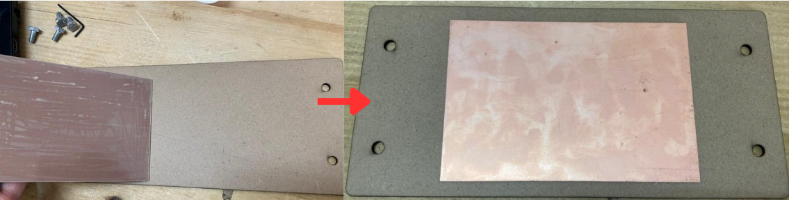
- Securing the PCB material to the bed.
- Setting the X, Y, and Z origin points.
- Loading the .rml files in the correct order.
- Running each process sequentially (drilling, traces, cutout).
- Changing tools and recalibrating Z between each step.
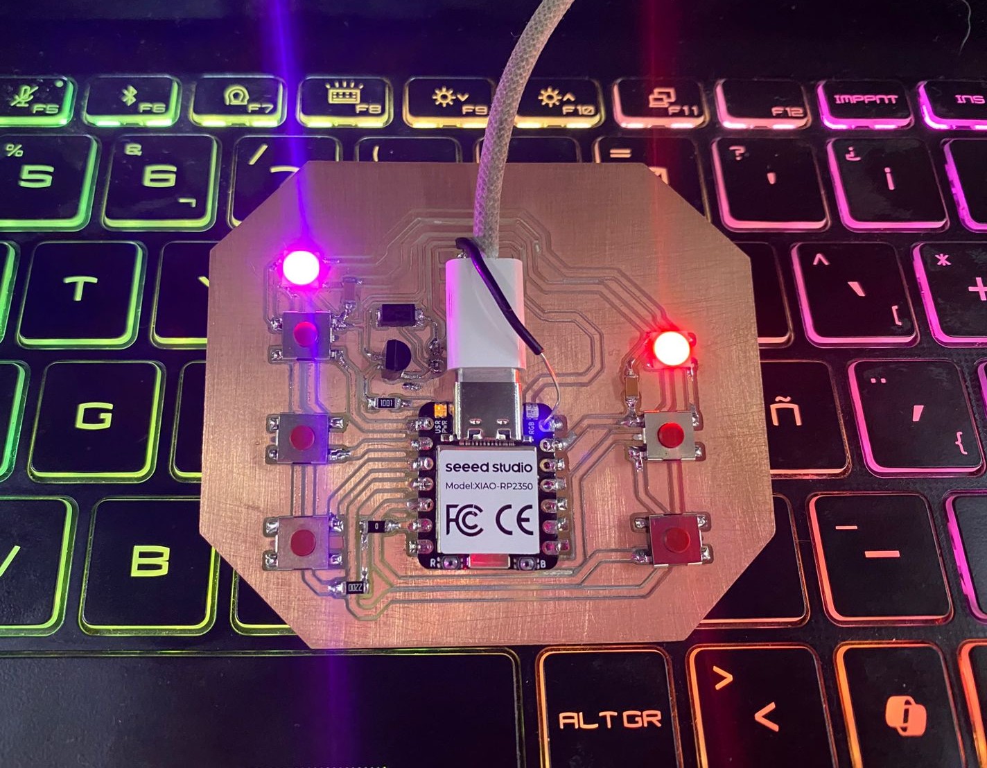
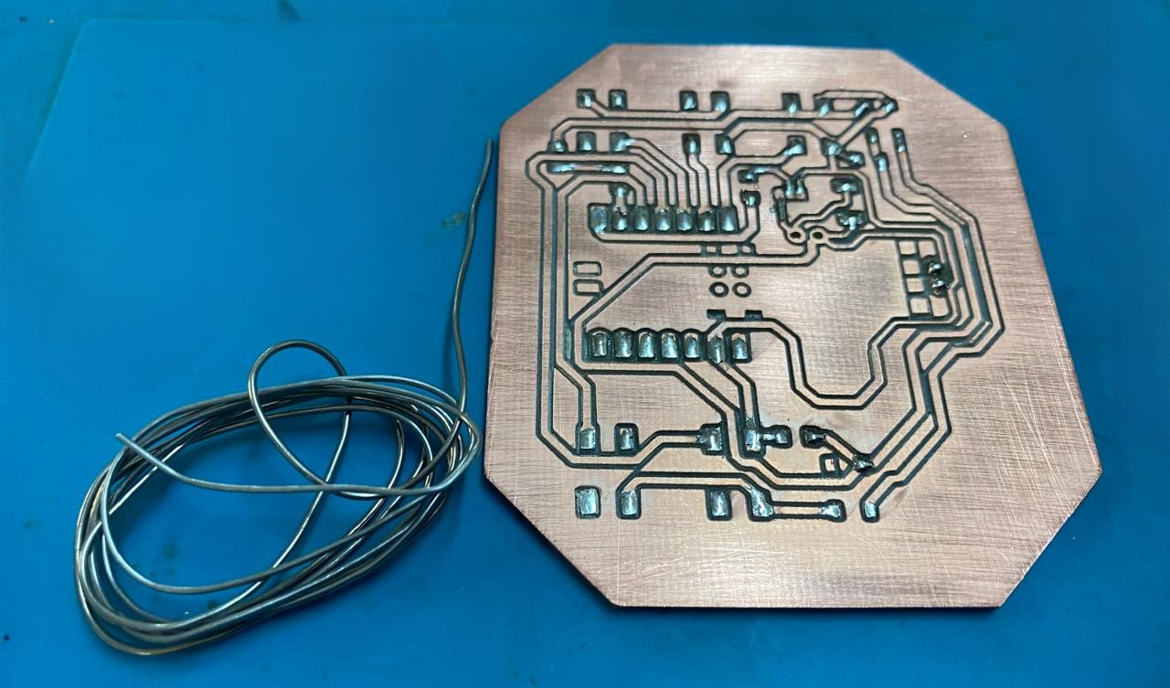
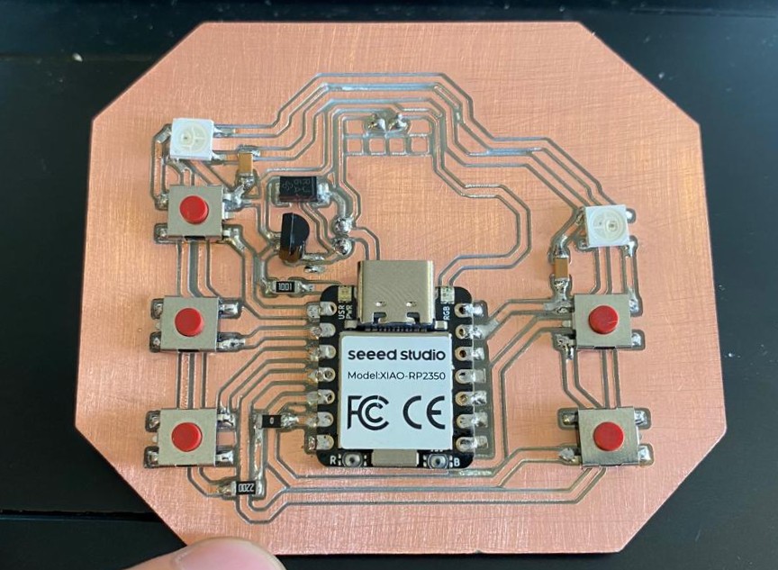
Solder
With the PCB already milled and cut, the next step is soldering. Since most of the components are SMD, it is necessary to pretin the pads before placing the components. This process consists of applying a small amount of solder to the pad by heating it with the soldering iron for a few seconds, and then feeding solder from the opposite side until it melts and forms a thin, even layer.Once the pad is pretinned, the component can be positioned and soldered by reheating the pad and allowing the solder to secure it in place.
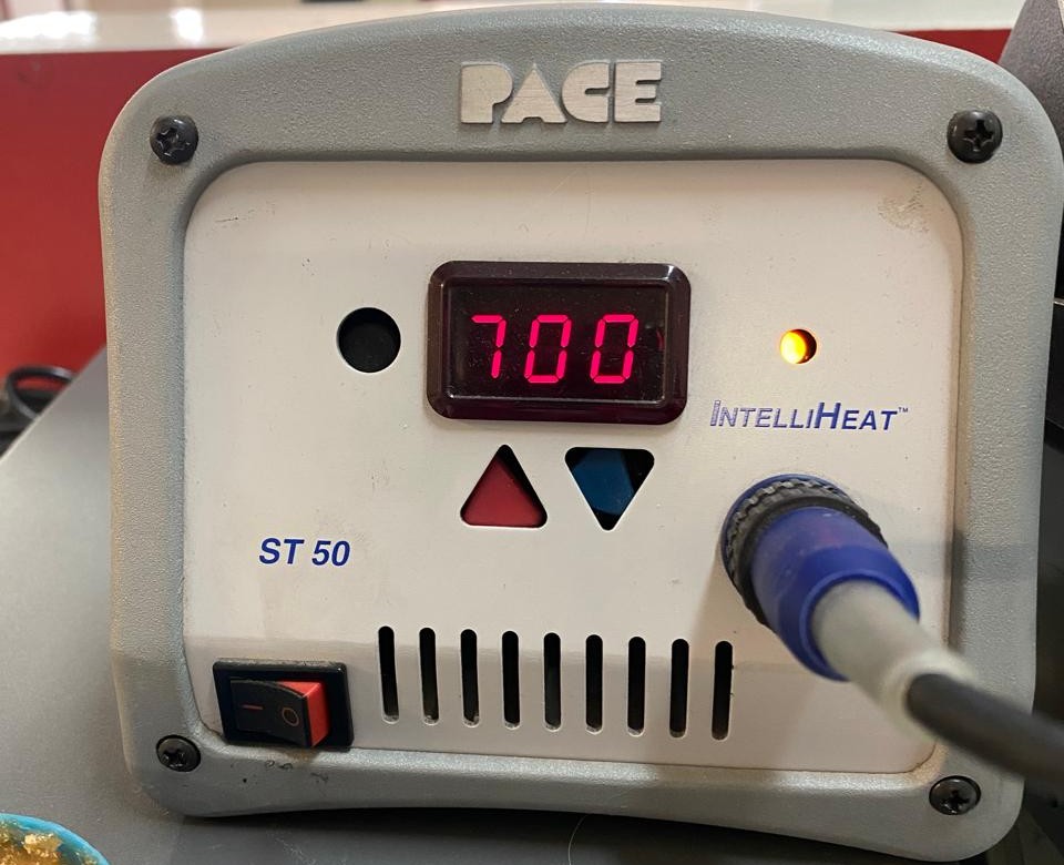
Soldering Temperatures
| Temperature (°F) | Application |
|---|---|
| 600–650°F | Delicate components, low thermal mass |
| 650–700°F | General SMD soldering (recommended range) |
| 700–750°F | Through-hole components or larger pads |
| 750°F+ | Heavy ground planes (use with caution) |
- Capacitors and resistors (smallest components)
- LEDs (SMD)
- Buttons and connectors
- Microcontroller (XIAO RP2040)
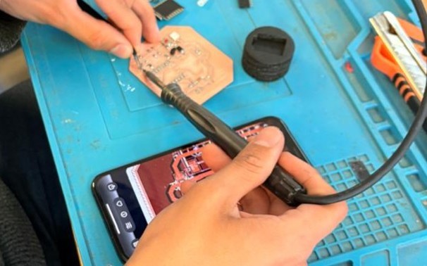
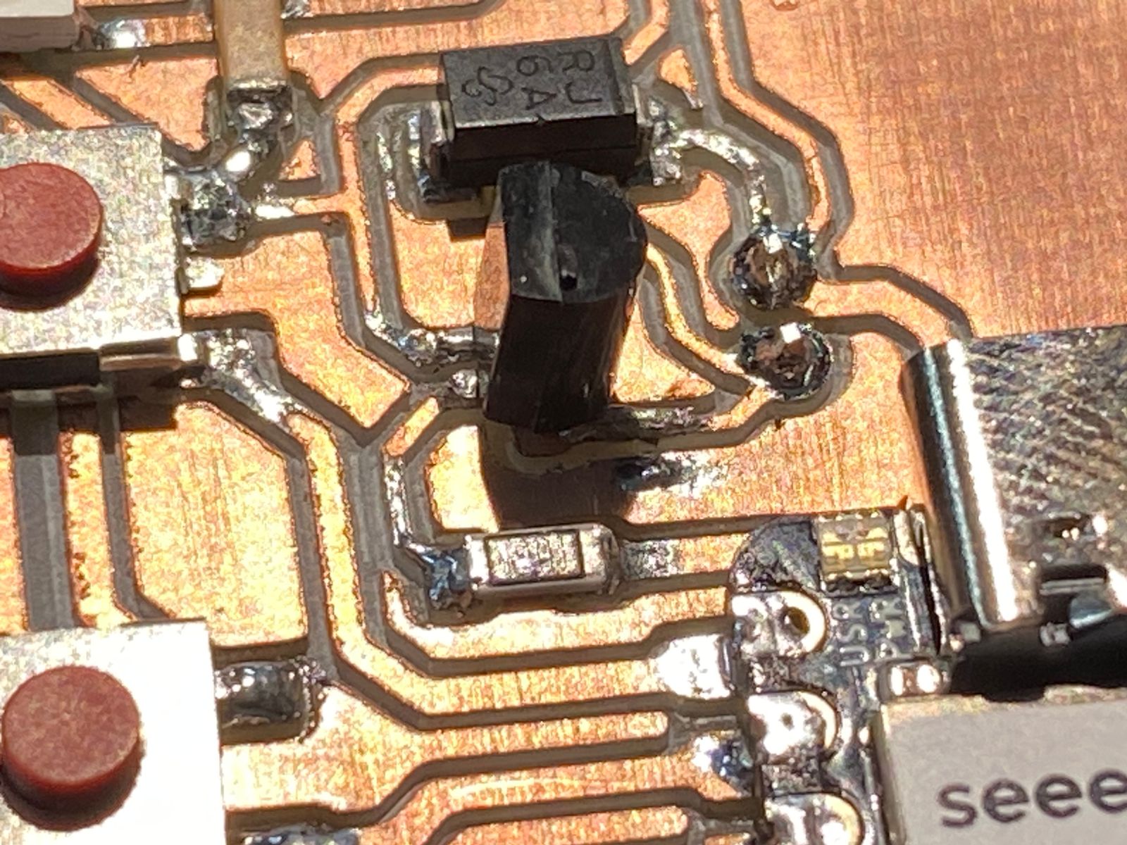
Problems
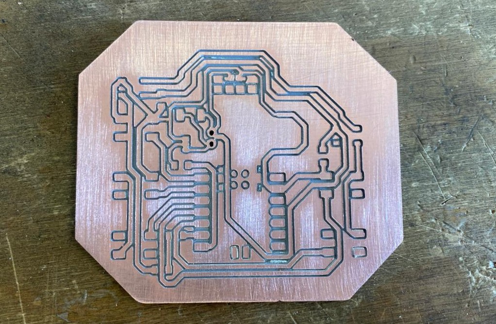
Most of the issues encountered during fabrication were related to tool limitations during the milling process. In some cases, the milling bits were not fine enough to properly isolate the traces, causing them to remain partially connected.- When traces are unintentionally shorted, a practical solution is to carefully use a precision knife (cutter) to remove excess copper and separate the tracks.
However, this modification has several implications:
- Reduced mechanical strength, making the component more fragile.
- Higher risk of poor electrical contact due to smaller soldering area.
- Potential long-term reliability issues, especially under vibration or stress.
Code
Results
In my computer and gameplay